Article

Unraveling Mass Transfer and Reaction Processes in CVD-Grown MoS2 Films: A Multiphysical Field Coupling Study

State Key Laboratory of Advanced Technology for Materials Synthesis and Processing, Wuhan University of Technology, Wuhan 430070, China
*
Authors to whom correspondence should be addressed.
These authors contributed equally to this work.
Appl. Sci. 2025, 15(5), 2627; https://doi.org/10.3390/app15052627
Submission received: 11 February 2025 / Revised: 26 February 2025 / Accepted: 27 February 2025 / Published: 28 February 2025

Abstract

:
The two-dimensional semiconductor material MoS2, grown via chemical vapor deposition, has shown significant potential to surpass silicon in advanced electronic technologies. However, the mass transfer and chemical reaction processes critical to the nucleation and growth of MoS2 grains remain poorly understood. In this study, we conducted an in-depth investigation into the mass transfer and chemical reaction processes during the chemical vapor deposition of MoS2, employing a novel multi-physics coupling model that integrates flow fields, temperature fields, mass transfer, and chemical reactions. Our findings reveal that the intermediate product Mo3O9S4 not only fails to participate directly in MoS2 film growth but also hinders the diffusion of MoS6, limiting the growth process. We demonstrate that increasing the growth temperature accelerates the diffusion rate of MoS6, mitigates the adverse effects of Mo3O9S4, and promotes the layered growth of MoS2 films. Additionally, lowering the growth pressure enhances the convective diffusion of reactants, accelerating grain growth. This research significantly advances our understanding of the mass transport and reaction processes in MoS2 film growth and provides critical insights for optimizing chemical vapor deposition systems.

1. Introduction

With the rapid development of the integrated circuit industry, device density and performance continue to increase, causing channel sizes, which represent the characteristic length of field-effect transistors, to approach physical limits. This makes it difficult for silicon to sustain Moore’s Law, which predicts the doubling of transistor density every two years [1]. As transistors approach atomic scales, alternative materials are needed to overcome challenges in power consumption, heat dissipation, and short-channel effects. Two-dimensional (2D) materials, such as graphene, black phosphorus, and transition metal dichalcogenides (TMDs), have emerged as promising candidates for next-generation electronic devices due to their unique properties [2]. Among 2D materials, MoS2 stands out due to its semiconducting nature, tunable bandgap, high carrier mobility, and mechanical flexibility, offering unique advantages in short-channel applications [3,4,5,6,7,8,9,10,11]. As a result, achieving the controllable growth of MoS2 thin films has become an urgent and shared goal in both academic and industrial sectors. Researchers have developed various methods to obtain high-quality MoS2 thin films, including physical vapor deposition (PVD) [12,13,14,15], metal-organic chemical vapor deposition (MOCVD) [16,17,18], and chemical vapor deposition (CVD) [19,20,21]. Among these methods, CVD has shown great potential for large-scale MoS2 film production due to its high efficiency, low cost, and ability to produce high-quality films.
During the CVD growth of MoS2 thin films, various process parameters—such as temperature, pressure, gas flow rate, substrate condition, and precursor type—collectively influence the transport, reaction, and nucleation/growth processes of the reactants [22,23,24,25,26,27,28]. By precisely controlling these parameters, the morphology, size, orientation, and phase structure of the thin films can be effectively tailored, enabling the fabrication of MoS2 films with tunable properties to meet the demands of different applications. Currently, research on the growth mechanisms of MoS2 films primarily focuses on the effects of substrate surface properties—such as surface symmetry, step edges, buffer layers, and surface defects—on nucleation and growth [29]. However, the understanding of the growth conditions that directly influence material nucleation and growth remains largely empirical, relying on trial-and-error approaches [19,20,21]. In particular, mass transport and reaction processes, which are directly linked to growth conditions, have not been investigated in depth. Therefore, a systematic study of the flow field, temperature field, mass transfer, and reaction processes during MoS2 film growth is crucial for a deeper understanding of the growth mechanism and for achieving controlled fabrication of these thin films.
In this study, we established a multiphysics coupling model involving the flow field, temperature field, mass transport, and chemical reactions, and thoroughly analyzed the effects of temperature and pressure on the growth of MoS2 films. We found that the intermediate product Mo3O9S4 is the key factor limiting the reaction rate, which not only cannot directly participate in the growth of MoS2 film, but also hinders the diffusion of MoS6, thus impeding film growth. Increasing the growth temperature can accelerate the diffusion rate of MoS6 and weaken the influence of Mo3O9S4, enabling the layered growth of MoS2 thin films. Simultaneously, lowering the growth pressure can accelerate the convective diffusion rate of the reactants, promoting grain growth. When the pressure is reduced from 100 Torr to 10 Torr, the grain size of the MoS2 film increases from 10 μm to 50 μm. This study deepens our understanding of the mass transport and reaction processes in the CVD growth of MoS2 films.

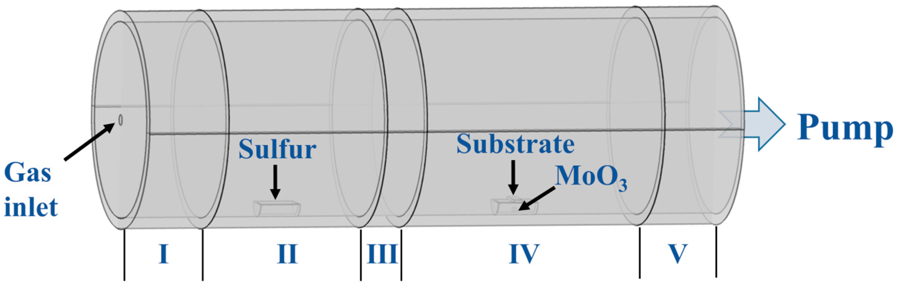
2. Experimental Methods

The growth of MoS2 films was conducted in a low-pressure dual-zone CVD system with an 80 mm diameter tube, as shown in Figure S1a. Elemental S powder (5 g, 99.95%, Aladdin) and MoO3 powder (60 mg, 99.95%, Aladdin) were placed in two separate quartz crucibles, positioned at the centers of two distinct temperature zones, with a 30 cm distance between them. A 300 nm-thick Si/SiO2 substrate (1 × 1 cm2) was ultrasonically cleaned with acetone, isopropyl alcohol, and deionized water, followed by nitrogen blow drying. The substrate was placed face-down on the MoO3 powder, with a distance of approximately 3 mm between the MoO3 and the substrate. The temperature of the S powder was set to 423 K, while the temperatures of the MoO3 was set to 1033 K, 1053 K, and 1073 K, respectively. The heating rate was 10 K/min, ensuring that both the S and MoO3 powders reached their target temperatures simultaneously. Throughout the growth process, a continuous Ar gas flow of 200 sccm was maintained, with the system pressure was set to 10, 40, 70, and 100 Torr via a gate valve.
The optical microscopy images of MoS2 films were obtained using the BX53M optical microscope from Olympus (Tokyo, Japan). The Raman and photoluminescence (PL) spectra of the samples were measured using the LabRAM Odyssey confocal Raman spectrometer from HORIBA Scientific (Kyoto, Japan) with a ×50 long working distance objective, excited at a wavelength of 532 nm, and a grating density of 600 gr/mm.

3. Construction of Multiphysics Coupling Model

In the CVD system, the entire reaction process involves multiple coupled physical fields, including the flow field, temperature field, mass transfer of trace species, and chemical reactions. The flow field and temperature field are interrelated and form the foundation for mass transfer and chemical reactions. Therefore, we first developed a coupled flow and temperature field model using COMSOL Multiphysics 6.1 software. Based on the results of the flow and temperature fields, we then performed coupled calculations for mass transfer and chemical reactions. The flowchart of the simulation and calculation process is shown in Figure S2. The finite element geometry model is shown in Figure 1, and the detailed modeling process is provided in the Supplementary Information.
The precursor sulfur and MoO3 source need to undergo a series of elementary reactions to form the final product MoS2. Previous studies, combining molecular dynamics and first-principles calculations, have outlined the reaction pathway for sulfur and MoO3. Elemental sulfur evaporates to form S2 dimers that participate in the reaction, while MoO3 evaporates to produce the gaseous precursor Mo3O9 [30]. The initial gaseous reactants are S2 and Mo3O9, which undergo the following reactions:
Mo 3 O 9 + S 2 1.31   eV 0.79   eV Mo 3 O 9 S 2
Mo 3 O 9 S 2 + S 2 1.11   eV 0.81   eV Mo 3 O 9 S 4
Mo 3 O 9 S 4 + S 2 0.42   eV 0.95   eV Mo 2 O 6 S 4 + MoO 3 S 2
MoO 3 S 2 + S 2 1.61   eV 0.61   eV MoO 3 S 4
MoO 3 S 4 + S 2 1.25   eV 0.43   eV MoO 2 S 4 + S 2 O
MoO 2 S 4 + S 2 0.52   eV 0.37   eV MoOS 4 + S 2 O
MoOS 4 + S 2 1.30   eV 0.46   eV MoOS 6
MoOS 6 + S 2 1.30   eV 0.46   eV MoS 6 + S 2 O
MoS 6 MoS 2 ( monolayer ) + S 4
The energy in these equations represents the transition state energy barrier that must be overcome for the reaction to proceed. For most reactions, the forward reaction is more favorable, facilitating the reaction process. However, the reaction between Mo3O9S4 and S2 limits the overall reaction rate, meaning that modulation of this step can significantly affect the entire process. Finally, MoS6 serves as the final gaseous intermediate product, which forms monolayer MoS2 on the substrate.
Based on transition state theory, the reaction rate for these elementary steps can be calculated [31,32]. To model this process, we used the reaction engineering module in the COMSOL software. In a 1 m3 reactor with the temperature set at 1053 K and initial concentrations of S2 and Mo3O9 at 1 mol/m3 and 0.001 mol/m3, respectively, the concentration changes of reactants and intermediate products over time were simulated, as shown in Figure S1b. The results demonstrate that the entire reaction process is essentially completed within 100 ns. The reaction of the intermediate product Mo3O9S4 is identified as the key step that limits the overall reaction rate of the process. Therefore, this study takes S2 and Mo3O9 as the initial reactants, MoS6 as the product, and further investigates the impact of temperature and flow fields on the reaction dynamics.

4. Results and Discussion

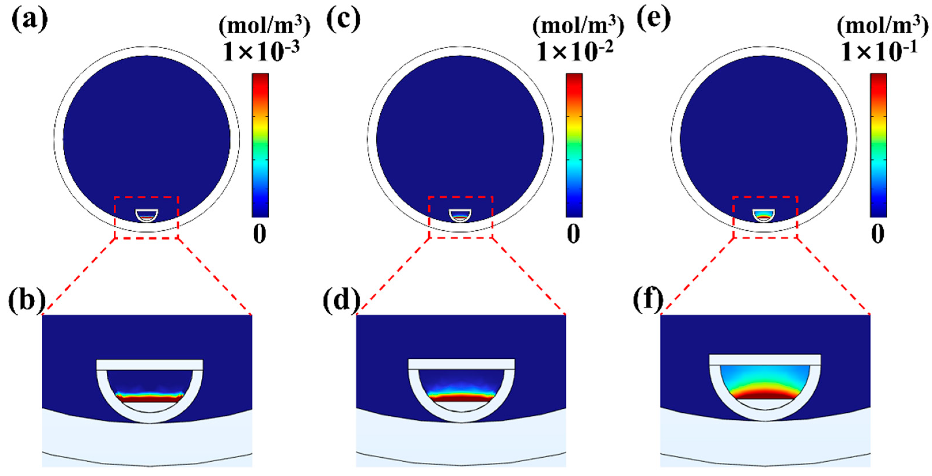
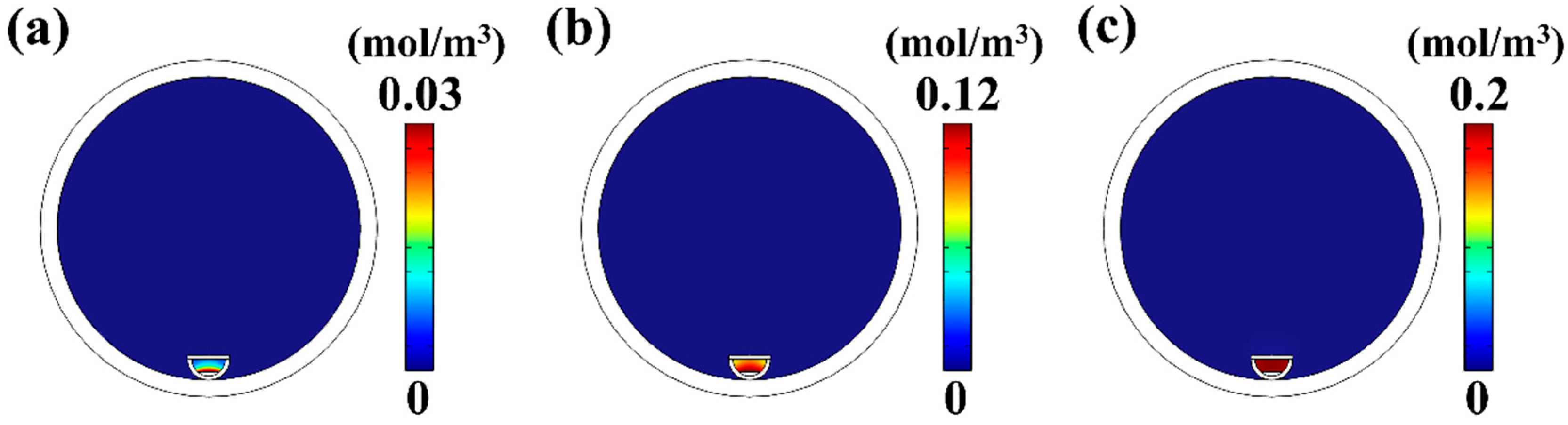
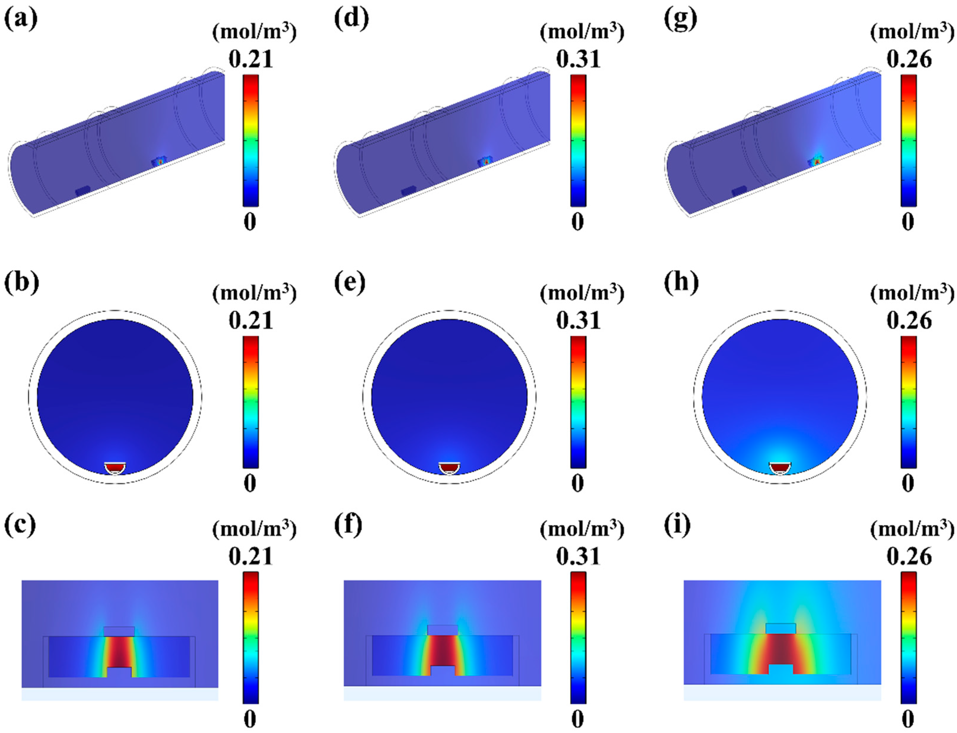
4.1. The Influence of Temperature on MoS2 Growth

The growth temperature plays a crucial role in influencing the volatility and reactions of precursors, as well as the nucleation and growth processes of MoS2 films. Figure 2a–c presents optical microscopy images of MoS2 films grown at 1033 K, 1053 K, and 1073 K under a fixed pressure of 70 Torr. At 1033 K, irregular and fluffy structures are observed on the substrate surface, with no well-defined grains. As the growth temperature increases to 1053 K, triangular-shaped MoS2 grains appear on the surface, and with further temperature elevation, the grain size gradually increases. Thicker crystal nuclei can be observed at the center of some grains, indicating island-like growth of the MoS2 films.
The XPS data for the sample grown at 1053 K and 70 Torr are shown in Figure S3. The Mo 3d3/2 and Mo 3d5/2 peaks appear at 233.0 eV and 229.9 eV, suggesting the 4+ oxidation state of Mo. An additional peak at 227.1 eV corresponds to the S 2s state. Figure S3b shows that S 2p3/2 and S 2p1/2 peaks appear at 163.9 eV and 162.7 eV, indicating the 2-oxidation state of sulfur. This provides confirmation of the formation of MoS2.
The interlayer interactions in MoS2 films are influenced by the film thickness, resulting in a thickness-dependent characteristic of the vibrational mode frequencies. Figure 2d presents the Raman spectra of MoS2 films grown at different temperatures. The Raman frequency difference between the E2g1 and A1g modes for the MoS2 films grown at 1053 K and 1073 K are 21.1 cm−1 and 21.4 cm−1, respectively, which corresponds to the bilayer MoS2 films, indicating the presence of small crystallites on top of the monolayer MoS2. For the MoS2 film grown at 1033 K, the frequency difference is 26.3 cm−1, suggesting that the film thickness has exceeded four layers [33]. Figure 2e presents the PL spectra of MoS2 films grown at different temperatures. It includes a strong A-excitonic peak around 681 nm and a weak B-excitonic peak around 632 nm. The A-excitonic peak is highly sensitive to the film’s quality and thickness [34]. As the film thickness increases, the intensity of the A-excitonic peak undergoes quenching.
The following section focuses on analyzing the impact of temperature on the reaction process. First, temperature affects the evaporation rates of S2 and Mo3O9. In this study, the evaporation rates of S2 and Mo3O9 were obtained by measuring the consumption of sulfur (S) and MoO3. At a pressure of 70 Torr and a temperature of 423 K, the evaporation rate of S2 was 1.26 × 10⁻³ mol min−1 cm−2. Additionally, the evaporation rate of MoO3 was tested at different temperatures under a pressure of 70 Torr, as shown in Table 1. As the temperature increased, the evaporation rate of Mo3O9 rapidly increased from 1.9 × 10⁻⁴ mol min−1 cm−2 at 1033 K to 6.6 × 10⁻⁴ mol min−1 cm−2 at 1073 K.
Based on the experimental conditions, the finite element model was set up with the temperatures of the IV region at 1033 K, 1053 K, and 1073 K for calculation. Figure S4 shows the temperature distribution in the CVD system along with the cross-sectional temperature distribution at the center of the substrate. At a set temperature of 1033 K, the substrate temperature is only 884 K. This is because the gas flow carries away additional heat as it passes over the substrate. As the set temperature increases, the substrate temperature also rises, but the temperature difference between the set temperature and the substrate temperature gradually becomes larger. At a set temperature of 1073 K, the substrate temperature increases to 915 K, with a temperature difference of 158 K.
Figure S5 present the velocity distribution and the cross-sectional velocity distribution at the center of the substrate under different set temperatures. Since the gas is in a laminar flow state, the flow velocity is higher at the center of the chamber. At a set temperature of 1033 K, the gas velocity at the inlet reaches a maximum of approximately 4.6 m/s. After entering the chamber, the velocity quickly decreases, with the flow velocity at the rear of the first temperature zone dropping to 0.03 m/s. When the gas transitions from the low-temperature zone to the high-temperature zone, the velocity increases rapidly, reaching 0.07 m/s at the center. This is due to the reduced gas density caused by the higher temperature. However, it is noteworthy that as the set temperature increases, the change in gas velocity is minimal. Inside the crucible, the maximum gas velocity at the center is only about 0.001 m/s. Moreover, since the gas is in laminar flow, the gas velocity at the surface of the substrate is nearly zero, which helps create a relatively stable growth environment. This reduces the interference of the carrier gas on the nucleation and growth processes.
The distribution of the flow field and temperature field determines the convective and diffusive rates of S2 and Mo3O9, which in turn influences their concentration distribution after evaporation. Under different growth temperatures, the concentration distribution of S2 is shown in Figure S6. In the heated evaporation region, S2 exhibits an uneven concentration distribution. Upon entering the high-temperature zone, the concentration of S2 becomes uniformly distributed due to the high diffusion rate induced by the elevated temperature, reaching approximately 2.60 mol/m3. As S2 reaches the precursor MoO3, it begins to react with the gaseous precursor Mo3O9 and intermediate products, leading to a decrease in S2 concentration. At growth temperatures of 1033 K, 1053 K, and 1073 K, the concentrations of S2 at the substrate position are 1.32, 0.40, and 0.48 mol/m3, respectively.
The increase in temperature leads to a rise in the evaporation rate of Mo3O9, which causes its concentration to increase inside the crucible, primarily concentrated above the precursor, as shown in Figure 3. At growth temperatures of 1033 K and 1053 K, the concentration of Mo3O9 at the substrate position is 0 mol/m3, indicating that the reaction between Mo3O9 and S2 is completed rapidly. However, when the growth temperature is increased to 1073 K, the concentration of Mo3O9 at the substrate position rises to 0.03 mol/m3. This is mainly due to the fact that with the further increase in temperature, the reverse reaction rates of the intermediate products Mo2O6S4 and MoO3S2 are accelerated, which limits the progression of the reaction, preventing the complete reaction of Mo3O9 and S2 and causing an increase in their concentrations at the substrate position.
After the reaction of Mo3O9 with S2, intermediate products are rapidly formed. Figure 4 shows the concentration distribution of Mo3O9S4 under different growth temperatures at a pressure of 70 Torr. As the set temperature increases from 1033 K to 1073 K, the concentration of Mo3O9S4 at the substrate position increases significantly from 0.006 mol/m3 to 0.24 mol/m3. This can be attributed to both the increased evaporation rate of Mo3O9 and the accelerated reverse reaction rates of Mo2O6S4 and MoO3S2. The concentration distributions of other intermediate products at a pressure of 70 Torr and a temperature of 1053 K are shown in Figure S7. The concentrations of all intermediate products are concentrated above the precursor inside the crucible, and the concentrations at the substrate position are significantly lower, indicating that the reaction proceeds rapidly. The concentration of Mo3O9S4 is approximately 0.09 mol/m3, much higher than that of other intermediate products (e.g., the concentration of MoO3S2 is 1 × 10⁻⁴ mol/m3). This suggests that the reaction involving Mo3O9S4 is the rate-limiting step for the entire reaction.
Figure 5 shows the concentration distribution of MoS6 products at different growth temperatures. At 1033 K, 1053 K, and 1073 K, the concentration of MoS6 at the substrate position is 0.19 mol/m3, 0.31 mol/m3, and 0.24 mol/m3, respectively. As the temperature increases, the evaporation rate of Mo3O9 rises, while the reverse reaction rates of Mo2O6S4 and MoO3S2 accelerate, resulting in a non-monotonic change in the concentration of MoS6. Figure 5c,f,i shows a symmetric distribution of MoS6 concentration along the center of the substrate inside the crucible, indicating that the diffusion of reactants is the dominant factor in the mass transfer process within the crucible. This is mainly due to the relatively low gas flow rate inside the crucible.
Based on the above observations, the state of the substrate can be summarized as follows: During the early stages of growth, the substrate surface is characterized by the coexistence of both MoS6 and Mo3O9S4. MoS6, as the final reactant before MoS2 film growth, directly contributes to the formation of the MoS2 film after diffusing to the edges of the MoS2 grains. In contrast, the intermediate product Mo3O9S4 not only fails to directly participate in the MoS2 film growth but also obstructs the diffusion of MoS6, hindering overall film growth, as shown in Figure S8. At low substrate temperatures, the diffusion rate of MoS6 is also low, and Mo3O9S4 severely restricts its diffusion. This results in a thicker film with a substrate surface covered by irregular and fluffy MoS2, which prevents the MoS2 from growing layer by layer. As the substrate temperature increases, although the concentration of Mo3O9S4 rises, the diffusion rate of MoS6 increases and the hindrance caused by Mo3O9S4 decreases. This enables MoS6 to diffuse more effectively to the vicinity of the nucleus, promoting the growth of a well-ordered MoS2 film. It is important to note that the MoS6 precursor undergoes an exothermic reaction on the substrate, forming MoS2 and releasing S4, without involving a transition state. As a result, we believe that temperature has a minimal effect on the growth rate.

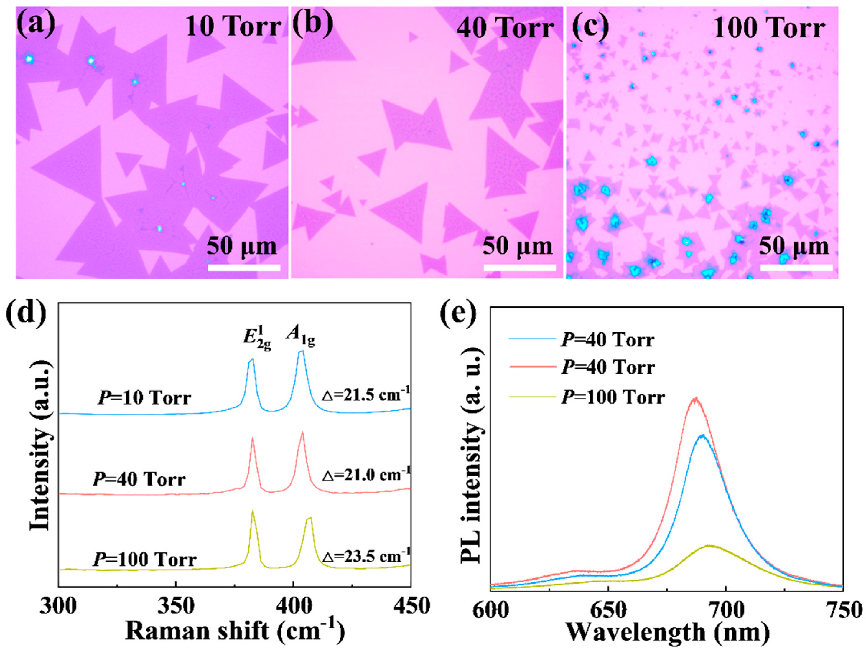
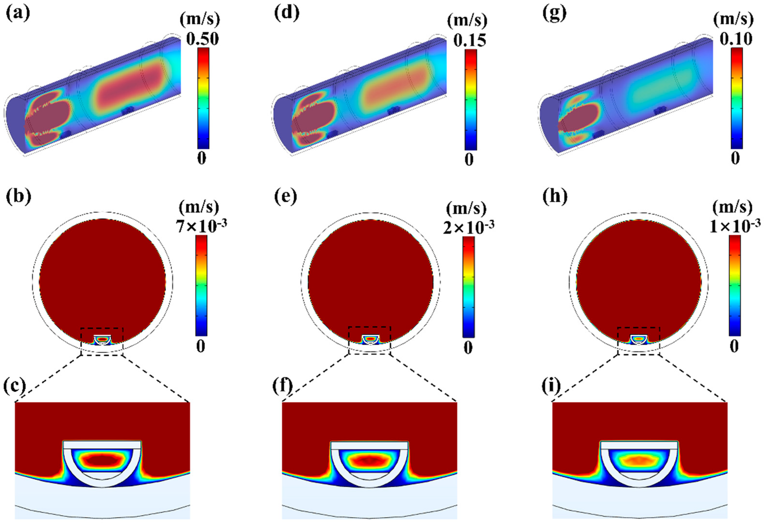
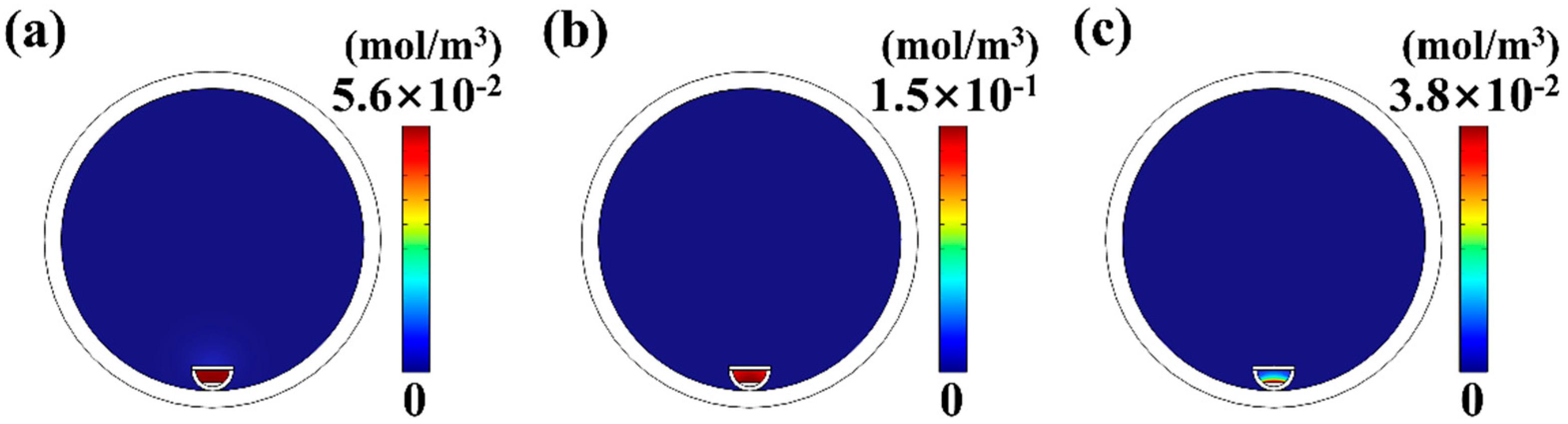
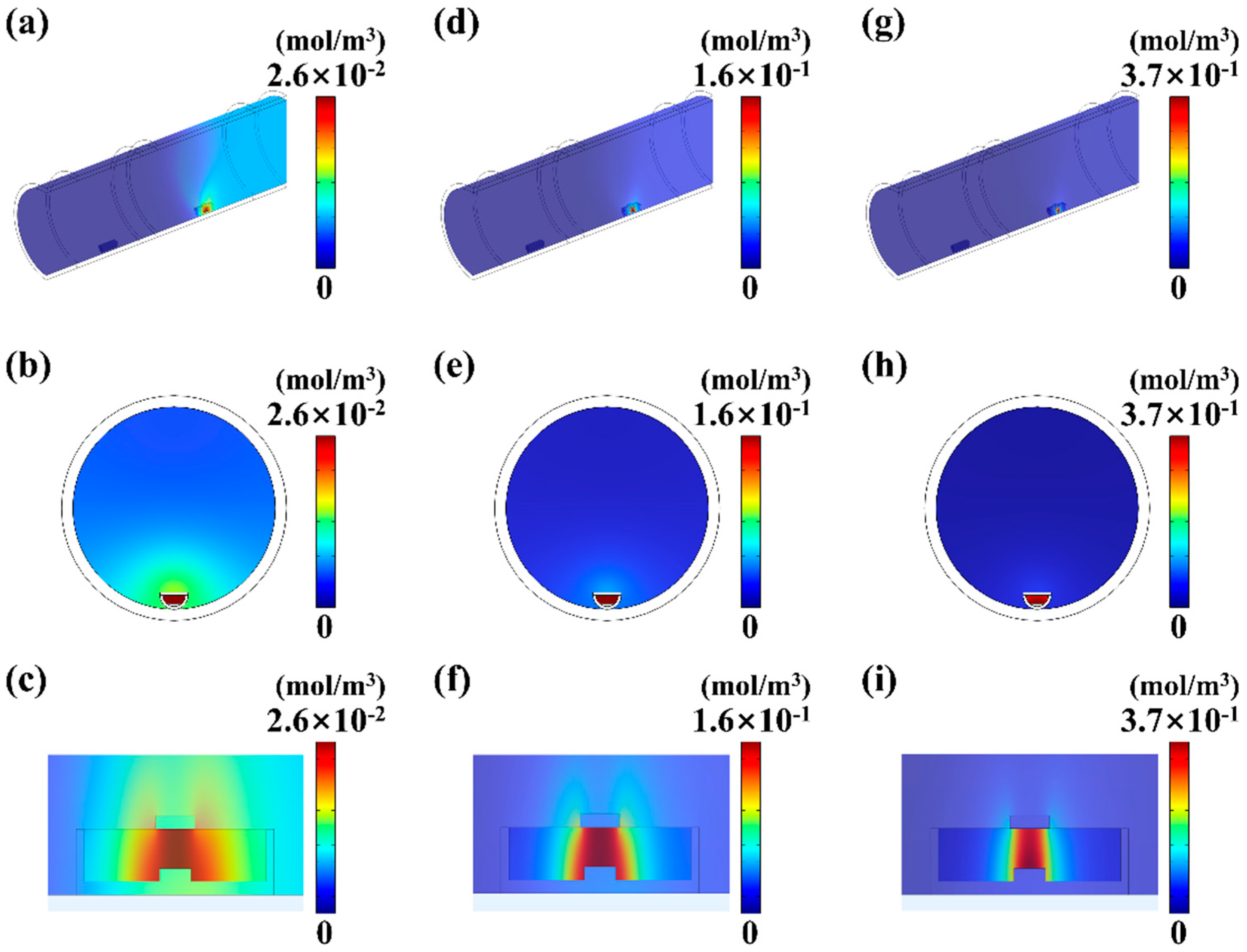
4.2. The Influence of Pressure on MoS2 Growth

Since pressure can significantly alter the flow field, thereby affecting the concentration of reactants and the reaction rate, we further investigate the influence of pressure. In this section, the growth temperature is fixed at 1053 K, and the impact of different pressures (10 Torr, 40 Torr, 70 Torr, and 100 Torr) on the growth of MoS2 films is explored, with results at 70 Torr presented in the above section. Figure 2b and Figure 6a–c show optical micrographs of samples grown under different pressures. As the pressure increases, the grain size gradually decreases. At 10 Torr, the grain size can reach up to 50 μm, whereas at 100 Torr, it shrinks to approximately 10 μm. Additionally, at both 10 Torr and 100 Torr, some grain centers exhibit distinctly thicker nuclei.
Figure 6d presents the Raman spectra of MoS2 films grown under different pressures. For films grown at pressures below 70 Torr, the wavenumber difference between the E2g1 and A1g peaks is less than 22 cm−1, indicating the presence of bilayer MoS2 films. However, when the pressure increases to 100 Torr, this wavenumber difference rises to 23.5 cm−1, corresponding to the Raman wavenumber difference of trilayer MoS2. Figure 6e shows the PL spectra of the samples grown at different pressures. As the film thickness increases, the PL intensity significantly decreases, accompanied by a slight red shift. This is due to the stronger interlayer interactions caused by the increased thickness, which leads to a reduction in the bandgap.
Not only does temperature affect the volatility rate of Mo3O9, but pressure also plays a crucial role in influencing its volatility rate. Table 2 shows the volatility rate of Mo3O9 at different pressures when the temperature is 1053 K. As the pressure increases from 10 Torr to 100 Torr, the volatility rate of Mo3O9 rapidly decreases from 9.4 × 10⁻⁴ mol min−1 cm−2 to 2.4 × 10⁻⁴ mol min−1 cm−2. In contrast, the pressure has little effect on the volatility rate of S2, which remains relatively stable at 1.26 × 10⁻³ mol min−1 cm−2. Finite element simulations were then conducted based on these volatility rates.
Figure S9 illustrates the temperature distribution in the CVD system at different pressures, along with the cross-sectional temperature distribution at the center of the substrate. The results indicate that pressure has a minimal impact on the temperature. Although additional heat is carried away by the gas flowing through the substrate, varying the pressure does not affect the temperature distribution at the substrate when the gas flow rate remains constant. Figure 7 shows the flow velocity distribution in the CVD system at different pressures, as well as the cross-sectional flow velocity distribution at the center of the substrate. As pressure increases, the gas velocity rises significantly. At 10 Torr, the maximum gas velocities in the IV region and inside the crucible are 0.48 m/s and 0.008 m/s, respectively, while at 100 Torr, these values decrease to 0.05 m/s and 0.0008 m/s.
The variation in flow velocity has a significant impact on the convection process of mass transport, leading to a notable increase in the concentration of S2 within the chamber as pressure rises, as shown in Figure S10. At pressures of 10, 40, 70, and 100 Torr, the S2 concentrations at the substrate are 0.08, 0.17, 0.40, and 1.40 mol/m3, respectively. For Mo3O9, the concentration in both the crucible and substrate regions decreases as pressure increases, as shown in Figure 8. At pressures of 10 and 40 Torr, the Mo3O9 concentrations at the substrate are 0.025 and 0.004 mol/m3, respectively. As the pressure increases to 70 and 100 Torr, the Mo3O9 concentration at the substrate becomes 0 mol/m3. This decrease is partly due to the reduced evaporation rate of Mo3O9 at higher pressures and partly due to the accelerated reaction rate driven by the increased S2 concentration.
Figure 9 shows the concentration distribution of Mo3O9S4 at different pressures. As pressure increases, the concentration of Mo3O9S4 in the substrate region first increases and then decreases. On the one hand, the increase in pressure slows down the convection diffusion rate of the dilute species, causing the reaction in the substrate region to reach completion more quickly and raising the equilibrium concentration of Mo3O9S4 at the substrate. On the other hand, the increased pressure reduces the volatilization rate of Mo3O9, leading to a decrease in the concentration of the intermediate product Mo3O9S4. These two factors compete with each other, resulting in the concentration first increasing and then decreasing with rising pressure.
As the pressure increases, the concentration of MoS6 products within the chamber also increases, as shown in Figure 10. The concentration of MoS6 at the substrate position rises from 0.03 mol/m3 at 10 Torr to 0.35 mol/m3 at 100 Torr. Although the volatilization rate of Mo3O9 is faster at lower pressures, the higher diffusion rate at these pressures causes the reaction products to diffuse rapidly, thereby diluting the product concentration. Figure 10c,f,i demonstrates that the MoS6 concentration is symmetrically distributed along the substrate center at different pressures. Despite the accelerated gas flow at lower pressures, the diffusion process of dilute species within the crucible region still dominates mass transfer.
Therefore, reducing the pressure to increase the flow velocity accelerates the convective diffusion rate of dilute species and decreases the concentration of MoS6 at the substrate. On the one hand, the decreased concentration of MoS6 will slow the nucleation and growth rate of the MoS2 film; on the other hand, the increased diffusion rate facilitates the diffusion-driven growth of MoS6 on the substrate. Consequently, reducing the pressure promotes grain growth but inhibits nucleation. This explains why, at 100 Torr, MoS2 films have thicker layers and smaller grains, while at 10 Torr, the films exhibit significantly larger grains.

5. Conclusions

In summary, this study provides a comprehensive analysis of the dual-temperature CVD growth process of MoS2 films, integrating both experimental and simulated approaches to systematically examine the impact of various growth parameters on mass transfer, reaction dynamics, and film growth. The results reveal that during the growth process, the substrate surface exhibits a coexistence of MoS6 and Mo3O9S4. The intermediate product Mo3O9S4 not only fails to directly contribute to MoS2 film growth but also obstructs the diffusion of MoS6, hindering film formation. When the growth temperature is increased from 1033 K to 1053 K, the diffusion rate of MoS6 increases, and the inhibitory effect of Mo3O9S4 on MoS6 diffusion decreases, enabling the layered growth of MoS2 films. Furthermore, lowering the pressure accelerates the convective diffusion rate of dilute species, significantly influencing the location of chemical reactions and the distribution of reaction products, which promotes grain diffusion and growth. This study not only deepens our understanding of mass transfer and reaction processes during MoS2 growth but also provides valuable insights for the design and optimization of CVD systems.

Supplementary Materials

The following supporting information can be downloaded at: https://www.mdpi.com/article/10.3390/app15052627/s1, Figure S1: (a) Schematic diagram of the dual-temperature zone CVD system; (b) Concentration of reactants and intermediates as a function of time at a temperature of 1053 K.; Figure S2: Flowchart of modeling and calculation processes; Figure S3: XPS data of MoS2 film grown at 1053 K and 70 Torr; Figure S4: Temperature distribution of the system when the pressure is 70 Torr and the set temperatures in region IV are (a-c) 1033 K, (d–f) 1053 K, and (g–i) 1073 K, where (b, e, h) are the radial cross-sectional views at the center of the substrate, and (c, f, i) are the corresponding local magnifications; Figure S5: Velocity distribution of the system when the pressure is 70 Torr and the temperature in Zone IV is set to (a-c) 1033 K, (d-f) 1053 K, and (g–i) 1073 K, where (b, e, h) are the radial cross-sectional views at the center of the substrate, and (c, f, i) are the corresponding local enlargements; Figure S6: Concentration distribution of S2 at a pressure of 70 Torr, with the temperature in growth region set to (a) 1033 K, (b) 1053 K, and (c) 1073 K; Figure S7: Radial cross-section of the concentration distribution of reactants and intermediates at the center of the substrate when the temperature in Zone IV is set to 1053 K and the pressure is 70 Torr: (a) Mo3O9S2; (b) MoO3S2; (c) MoO3S4; (d) MoO2S4; (e) MoOS4; (f) MoOS6; Figure S8: Schematic of MoS2 film growth on SiO2/Si substrate; Figure S9: Temperature distribution of the system at a set temperature of 1053 K in Zone IV, with gas pressures of (a, b) 10 Torr, (c, d) 40 Torr, and (e, f) 100 Torr, where (b, d, f) show radial cross-sectional views at the center position of the substrate; Figure S10: Concentration distribution of S2 at a temperature of 1053 K in growth region with pressures of (a) 10 Torr, (b) 40 Torr, and (c) 100 Torr; Figure S11: (a) The relationship between Ar gas density and temperature and pressure; (b) The relationship between Ar gas thermal conductivity and temperature; Figure S12: The Reynolds number of the dual-temperature zone CVD when the pressure is 70 Torr and the argon flow rate is 200 sccm.

Author Contributions

Z.Y. and J.L. contributed equally to this work. Conceptualization, X.S. and X.T.; simulation, Z.Y., J.L. and Y.L.; investigation, Z.Y., Q.Z. (Qing Zhang) and S.H.; data curation, S.C., S.Z. and Y.Z.; writing—original draft preparation, Z.Y.; writing—review and editing, X.S. and X.T.; supervision, X.S., Q.Z. (Qingjie Zhang) and X.T.; project administration, X.S. and X.T. All authors have read and agreed to the published version of the manuscript.

Funding

This work was supported by the National Key Research and Development Program of China (Grant No. 2024YFF0505900), Natural Science Foundation of China (W2412066), and the 111 Project of China (Grant No. B07040).

Institutional Review Board Statement

Not applicable.

Informed Consent Statement

Not applicable.

Data Availability Statement

Data available on request due to restrictions. The data presented in this study are available on request from the corresponding author. The data are not publicly available.

Conflicts of Interest

There are no conflicts of interest to declare.

References

  1. Waldrop, M.M. The chips are down for Moore’s law. Nature 2016, 530, 144. [Google Scholar] [CrossRef] [PubMed]
  2. Vashishtha, P.; Abidi, I.H.; Giridhar, S.P.; Verma, A.K.; Prajapat, P.; Bhoriya, A.; Murdoch, B.J.; Tollerud, J.O.; Xu, C.; Davis, J.A.; et al. CVD-grown monolayer MoS2 and GaN thin film heterostructure for a self-powered and bidirectional photodetector with an extended active spectrum. ACS Appl. Mater. Interfaces 2024, 16, 31294. [Google Scholar] [CrossRef]
  3. Li, M.Y.; Su, S.K.; Wong, H.P.; Li, L.J. How 2D semiconductors could extend Moore's law. Nature 2019, 567, 169. [Google Scholar] [CrossRef] [PubMed]
  4. Migliato Marega, G.; Zhao, Y.; Avsar, A.; Wang, Z.; Tripathi, M.; Radenovic, A.; Kis, A. Logic-in-memory based on an atomically thin semiconductor. Nature 2020, 587, 72. [Google Scholar] [CrossRef]
  5. Kwak, D.; Polyushkin, D.K.; Mueller, T. In-sensor computing using a MoS2 photodetector with programmable spectral responsivity. Nat. Commun. 2023, 14, 4264. [Google Scholar] [CrossRef] [PubMed]
  6. Shen, P.-C.; Su, C.; Lin, Y.; Chou, A.-S.; Cheng, C.-C.; Park, J.-H.; Chiu, M.-H.; Lu, A.-Y.; Tang, H.-L.; Tavakoli, M.M.; et al. Ultralow contact resistance between semimetal and monolayer semiconductors. Nature 2021, 593, 211. [Google Scholar] [CrossRef]
  7. Liu, Y.; Duan, X.; Shin, H.-J.; Park, S.; Huang, Y.; Duan, X. Promises and prospects of two-dimensional transistors. Nature 2021, 591, 43. [Google Scholar] [CrossRef]
  8. Das, S.; Sebastian, A.; Pop, E.; McClellan, C.J.; Franklin, A.D.; Grasser, T.; Knobloch, T.; Illarionov, Y.; Penumatcha, A.V.; Appenzeller, J.; et al. Transistors based on two-dimensional materials for future integrated circuits. Nat. Electron. 2021, 4, 786. [Google Scholar] [CrossRef]
  9. Zhang, X.; Grajal, J.; Vazquez-Roy, J.L.; Radhakrishna, U.; Wang, X.; Chern, W.; Zhou, L.; Lin, Y.; Shen, P.-C.; Ji, X.; et al. Two-dimensional MoS2-enabled flexible rectenna for Wi-Fi-band wireless energy harvesting. Nature 2019, 566, 368. [Google Scholar] [CrossRef]
  10. Vashishtha, P.; Dash, A.; Prajapat, P.; Goswami, P.; Walia, S.; Gupta, G. Self-powered broadband photodetection of MoS2/Sb2Se3 heterostructure. ACS Appl. Opt. Mater. 2023, 1, 1952. [Google Scholar] [CrossRef]
  11. Vashishtha, P.; Dash, A.; Walia, S.; Gupta, G. Self-bias Mo–Sb–Ga multilayer photodetector encompassing ultra-broad spectral response from UV–C to IR–B. Opt. Laser Technol. 2025, 181, 111705. [Google Scholar] [CrossRef]
  12. Duan, X.; Wang, C.; Shaw, J.C.; Cheng, R.; Chen, Y.; Li, H.; Wu, X.; Tang, Y.; Zhang, Q.; Pan, A.; et al. Lateral epitaxial growth of two-dimensional layered semiconductor heterojunctions. Nat. Nanotechnol. 2014, 9, 1024. [Google Scholar] [CrossRef]
  13. Zhang, Z.; Chen, P.; Duan, X.; Zang, K.; Luo, J.; Duan, X. Robust epitaxial growth of two-dimensional heterostructures, multiheterostructures, and superlattices. Science 2017, 357, 788. [Google Scholar] [CrossRef]
  14. Sahoo, P.K.; Memaran, S.; Xin, Y.; Balicas, L.; Gutierrez, H.R. One-pot growth of two-dimensional lateral heterostructures via sequential edge-epitaxy. Nature 2018, 553, 63. [Google Scholar] [CrossRef]
  15. Zheng, B.; Ma, C.; Li, D.; Lan, J.; Zhang, Z.; Sun, X.; Zheng, W.; Yang, T.; Zhu, C.; Ouyang, G.; et al. Band alignment engineering in two-dimensional lateral heterostructures. J. Am. Chem. Soc. 2018, 140, 11193. [Google Scholar] [CrossRef] [PubMed]
  16. Cun, H.; Macha, M.; Kim, H.; Liu, K.; Zhao, Y.; LaGrange, T.; Kis, A.; Radenovic, A. Wafer-scale MOCVD growth of monolayer MoS2 on sapphire and SiO2. Nano Res. 2019, 12, 2646. [Google Scholar] [CrossRef]
  17. Zhu, H.; Nayir, N.; Choudhury, T.H.; Bansal, A.; Huet, B.; Zhang, K.; Puretzky, A.A.; Bachu, S.; York, K.; Mc Knight, T.V.; et al. Step engineering for nucleation and domain orientation control in WSe2 epitaxy on c-plane sapphire. Nat. Nanotechnol. 2023, 18, 1295. [Google Scholar] [CrossRef]
  18. Olding, J.N.; Henning, A.; Dong, J.T.; Zhou, Q.; Moody, M.J.; Smeets, P.J.M.; Darancet, P.; Weiss, E.A.; Lauhon, L.J. Charge separation in epitaxial SnS/MoS2 vertical heterojunctions grown by low-temperature pulsed MOCVD. ACS Appl. Mater. Interfaces 2019, 11, 40543. [Google Scholar] [CrossRef]
  19. Yu, H.; Huang, L.; Zhou, L.; Peng, Y.; Li, X.; Yin, P.; Zhao, J.; Zhu, M.; Wang, S.; Liu, J.; et al. Eight In. wafer-scale epitaxial monolayer MoS2. Adv. Mater. 2024, 36, 2402855. [Google Scholar] [CrossRef]
  20. Li, L.; Wang, Q.; Wu, F.; Xu, Q.; Tian, J.; Huang, Z.; Wang, Q.; Zhao, X.; Zhang, Q.; Fan, Q.; et al. Epitaxy of wafer-scale single-crystal MoS2 monolayer via buffer layer control. Nat. Commun. 2024, 15, 1825. [Google Scholar] [CrossRef]
  21. Liu, L.; Li, T.; Ma, L.; Li, W.; Gao, S.; Sun, W.; Dong, R.; Zou, X.; Fan, D.; Shao, L.; et al. Uniform nucleation and epitaxy of bilayer molybdenum disulfide on sapphire. Nature 2022, 605, 69. [Google Scholar] [CrossRef] [PubMed]
  22. Yu, H.; Liao, M.; Zhao, W.; Liu, G.; Zhou, X.J.; Wei, Z.; Xu, X.; Liu, K.; Hu, Z.; Deng, K.; et al. Wafer-scale growth and transfer of highly-oriented monolayer MoS2 continuous films. ACS Nano 2017, 11, 12001. [Google Scholar] [CrossRef] [PubMed]
  23. Wang, Q.; Li, N.; Tang, J.; Zhu, J.; Zhang, Q.; Jia, Q.; Lu, Y.; Wei, Z.; Yu, H.; Zhao, Y.; et al. Wafer-scale highly oriented monolayer MoS2 with large domain sizes. Nano Lett. 2020, 20, 7193. [Google Scholar] [CrossRef]
  24. Xu, X.; Guo, T.; Kim, H.; Hota, M.K.; Alsaadi, R.S.; Lanza, M.; Zhang, X.; Alshareef, H.N. Growth of 2D materials at the wafer scale. Adv. Mater. 2022, 34, 2018258. [Google Scholar] [CrossRef]
  25. Chen, L.; Liu, B.; Ge, M.; Ma, Y.; Abbas, A.N.; Zhou, C. Step-edge-guided nucleation and growth of aligned WSe2 on sapphire via a layer-over-layer growth mode. ACS Nano 2015, 9, 8368. [Google Scholar] [CrossRef] [PubMed]
  26. Zhang, L.; Dong, J.; Ding, F. Strategies, status, and challenges in wafer scale single crystalline two-dimensional materials synthesis. Chem. Rev. 2021, 121, 6321. [Google Scholar] [CrossRef]
  27. Xu, J.; Ho, D. Modulation of the reaction mechanism via S/Mo: A rational strategy for large-area MoS2 growth. Chem. Mater. 2021, 33, 3249. [Google Scholar] [CrossRef]
  28. Rajan, A.G.; Warner, J.H.; Blankschtein, D.; Strano, M.S. Generalized mechanistic model for the chemical vapor deposition of 2D transition metal dichalcogenide monolayers. ACS Nano 2016, 10, 4330. [Google Scholar] [CrossRef]
  29. Xia, Y.; Chen, X.; Wei, J.; Wang, S.; Chen, S.; Wu, S.; Ji, M.; Sun, Z.; Xu, Z.; Bao, W.; et al. 12-inch growth of uniform MoS2 monolayer for integrated circuit manufacture. Nat. Mater. 2023, 22, 1324. [Google Scholar] [CrossRef]
  30. Lei, J.; Xie, Y.; Yakobson, B.I. Gas-phase “prehistory” and molecular precursors in monolayer metal dichalcogenides synthesis: The case of MoS2. ACS Nano 2021, 15, 10525. [Google Scholar] [CrossRef]
  31. Zhang, L.-L.; Zheng, J.; Gu, J.; Huang, Z.; Lu, L.; Li, H.; Chen, Z.; Yang, S. High-efficiency purification of CH4 and H2 energy sources enabled by a phosphotungstic acid-supported Os single-atom catalyst. J. Mater. Chem. A 2023, 11, 24698. [Google Scholar] [CrossRef]
  32. Ren, L.-K.; Zhu, L.-F.; Qi, T.; Tang, J.-Q.; Yang, H.-Q.; Hu, C.-W. Performance of dimethyl sulfoxide and brønsted acid catalysts in fructose conversion to 5-hydroxymethylfurfural. ACS Catal. 2017, 7, 2199. [Google Scholar] [CrossRef]
  33. Li, H.; Zhang, Q.; Yap, C.C.R.; Tay, B.K.; Edwin, T.H.T.; Olivier, A.; Baillargeat, D. From Bulk to Monolayer MoS2: Evolution of raman scattering. Adv. Funct. Mater. 2012, 22, 1385. [Google Scholar] [CrossRef]
  34. Verma, A.K.; Rahman, M.A.; Vashishtha, P.; Guo, X.; Sehrawat, M.; Mitra, R.; Giridhar, S.P.; Waqar, M.; Bhoriya, A.; Murdoch, B.J.; et al. Oxygen-passivated sulfur vacancies in monolayer MoS2 for enhanced piezoelectricity. ACS Nano 2025, 19, 3478. [Google Scholar] [CrossRef]
Figure 1. Finite element geometric model of dual temperature zone CVD.
Applsci 15 02627 g001
Figure 2. Optical micrographs of the sample surface grown at (a) 1033 K, (b) 1053 K, and (c) 1073 K under a constant pressure of 70 Torr, along with the corresponding (d) Raman spectra and (e) PL spectra.
Applsci 15 02627 g002
Figure 3. Radial cross-section of Mo3O9 concentration distribution at the center of the substrate when the pressure is 70 Torr and the temperature in growth region is set to (a,b) 1033 K, (c,d) 1053 K, and (e,f) 1073 K.
Applsci 15 02627 g003
Figure 4. Radial cross-section of the concentration distribution of Mo3O9S4 at the center of the substrate when the temperature in growth region is set to (a) 1033 K, (b) 1053 K, and (c) 1073 K at a pressure of 70 Torr.
Applsci 15 02627 g004
Figure 5. Concentration distribution of MoS6 when the temperature in growth region is set to (ac) 1033 K, (df) 1053 K, and (gi) 1073 K at a pressure of 70 Torr, where (b,e,h) are the radial cross-sectional views at the center of the substrate and (c,f,i) are the axial cross-sectional views at the center of the substrate.
Applsci 15 02627 g005
Figure 6. Optical microscopic images of the sample grown at a growth temperature of 1053 K under (a) 10 Torr, (b) 40 Torr, and (c) 100 Torr, along with the corresponding (d) Raman spectra and (e) PL spectra.
Applsci 15 02627 g006
Figure 7. Velocity distribution diagrams of the system at a pressure of (ac) 10 Torr, (df) 40 Torr, and (gi) 100 Torr when the temperature is set to 1053 K in growth region, where (b,e,h) are radial cross-section diagrams at the center of the substrate and (c,f,i) are corresponding local magnified diagrams.
Applsci 15 02627 g007
Figure 8. Radial cross-sectional view of the Mo3O9 concentration distribution at the center of the substrate at a set temperature of 1053 K in growth region, with a pressure of (a,b) 10 Torr, (c,d) 40 Torr, and (e,f) 100 Torr.
Applsci 15 02627 g008
Figure 9. Radial cross-sectional view of Mo3O9S4 concentration distribution at the center of the substrate in growth region, with a temperature set at 1053 K and pressures of (a) 10 Torr, (b) 40 Torr, and (c) 100 Torr.
Applsci 15 02627 g009
Figure 10. Concentration distribution of MoS6 when the temperature is set to 1053 K in a growth region, with the gas pressure at (ac) 10 Torr, (df) 40 Torr, and (gi) 100 Torr, where (b,e,h) are the radial cross-sectional views at the center of the substrate and (c,f,i) are the axial cross-sectional views at the center of the substrate.
Applsci 15 02627 g010
Table 1. Relationship between the evaporation rate of Mo3O9 and temperature.
SourcePressureTemperatureMo3O9 Flow
MoO3 powder70 Torr1033 K1.9 × 10−4 mol min−1 cm−2
1053 K3.9 × 10−4 mol min−1 cm−2
1073 K6.6 × 10−4 mol min−1 cm−2
Table 2. Relationship between the evaporation rate of Mo3O9 and gas pressure.
SourcePressureTemperatureMo3O9 Flow
MoO3 powder10 Torr1053 K9.4 × 10−4 mol min−1 cm−2
40 Torr5.5 × 10−4 mol min−1 cm−2
70 Torr3.9 × 10−4 mol min−1 cm−2
100 Torr2.4 × 10−4 mol min−1 cm−2
Disclaimer/Publisher’s Note: The statements, opinions and data contained in all publications are solely those of the individual author(s) and contributor(s) and not of MDPI and/or the editor(s). MDPI and/or the editor(s) disclaim responsibility for any injury to people or property resulting from any ideas, methods, instructions or products referred to in the content.

