Review

An Overview of Emerging Nuclear Sensor Technologies: Challenges, Advancements and Applications

1
Department of Mathematics, Oregon State University, Corvallis, OR 97331, USA
2
Department of Physics, Oregon State University, Corvallis, OR 97331, USA
3
Nuclear Energy and Fuel Cycle Division, Oak Ridge National Laboratory, Oak Ridge, TN 37831, USA
*
Author to whom correspondence should be addressed.
Appl. Sci. 2025, 15(5), 2338; https://doi.org/10.3390/app15052338
Submission received: 8 January 2025 / Revised: 12 February 2025 / Accepted: 17 February 2025 / Published: 21 February 2025

Abstract

:
Nuclear sensors are essential for detecting and measuring nuclear radiation in various applications, including nuclear power plants, medical imaging, and environmental monitoring. Traditional nuclear sensors have served these fields for decades, but recent advancements in emerging sensor technologies offer novel improvements in accuracy, sensitivity, and reliability. This review presents an up-to-date overview of recent progress in the advancements of nuclear sensor technologies, their diverse applications, challenges in implementation, and opportunities for future research.

1. Introduction

Nuclear sensors are vital for detecting and measuring nuclear radiation in applications such as nuclear power generation, medical imaging, and environmental monitoring. However, while traditional sensors have been effective in these applications to date, recent technological advancements have led to the development of new sensor types, offering unique benefits and enhanced performance.
This review is novel in its comprehensive approach, integrating recent advances in material synthesis, device fabrication, and signal processing with a comparative analysis of four distinct sensor types. Moreover, while previous reviews (e.g., [1]) have focused on nuclear security measures and selected emerging technologies, our review fills a gap by critically evaluating the performance, scalability, and integration potential of these sensors across multiple application domains.
This review discusses graphene-based, quantum dot-based, neuromorphic-based, and solid-state nuclear sensors. Graphene-based sensors exploit graphene’s exceptional electrical and mechanical properties to achieve high sensitivity and rapid response times. Quantum dot-based sensors utilize semiconductor nanocrystals to provide a higher energy resolution in radiation detection. Neuromorphic-based sensors mimic neural network architectures to process radiation signals efficiently in real time. Solid-state (metal oxide) nuclear sensors have improved materials and fabrication techniques that enhance detection rates compared to conventional solid-state sensors.
The unique innovations offered by nuclear sensors include increased accuracy, sensitivity, and reliability, along with reduced size and cost. The fabrication of nuclear sensors has become more tangible due to recent advancements in fabrication techniques such as advanced manufacturing [2,3,4,5].
In nuclear power plants (NPPs), advanced sensor technology improves monitoring of reactors and cooling systems for early detection of anomalies [6]. In medical imaging, advanced sensor technology enhances the detection of gamma rays for precise localization of tumors [7]. Environmental monitoring benefits from nuclear sensor’s ability to detect low levels of radioactive contaminants in air, water, and soil [8].
Despite significant progress in the advancements of nuclear sensors, challenges remain in optimizing these technologies for widespread use. Issues such as scalability, integration with existing systems, and manufacturing costs need to be addressed. Ongoing research focuses on overcoming these obstacles to make the sensors more practical and accessible for industrial use.
This review presents an overview of recent advancements in graphene-based, quantum dot-based, neuromorphic-based, and solid-state nuclear sensors. It examines their advantages, limitations, and current development status. This paper also discusses challenges in the field and outlines future research directions.

2. Emerging Nuclear Sensor Technology

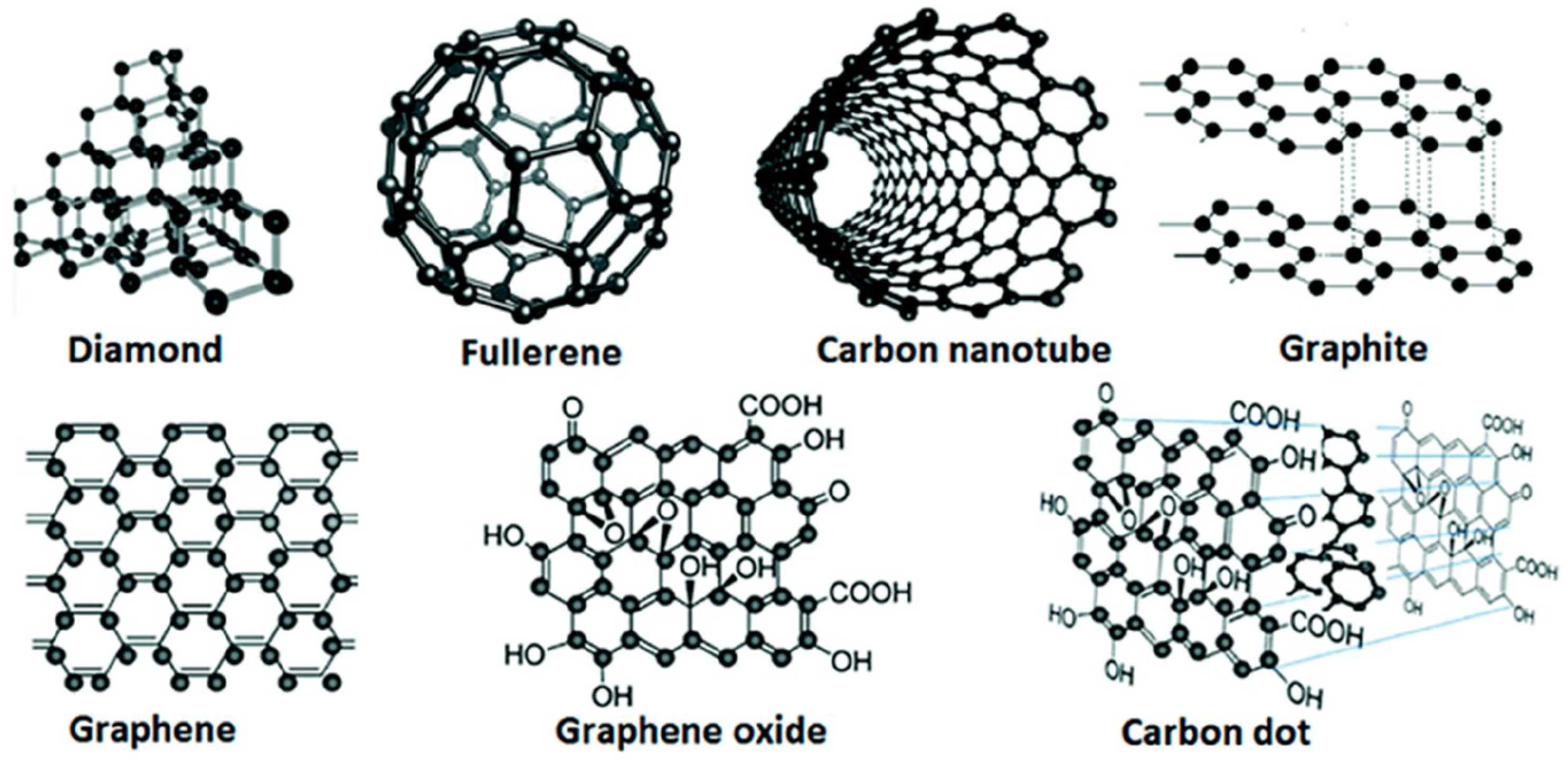
2.1. Graphene-Based Nuclear Sensors

Graphene is a one-atom-thick carbon allotrope with a hexagonal lattice structure (bottom left of Figure 1) that exhibits outstanding electrical, thermal, and mechanical properties. Its record-high carrier mobility (exceeding 200,000 c m 2 /Vs in ideal suspended films [9] and typically 10,000–50,000 c m 2 /Vs in supported layers [10]) and large theoretical specific surface area (approximately 2630 m 2 /g [11]) make graphene an excellent candidate for nuclear radiation detection. In sensor configurations—typically in field-effect transistor (FET) geometries—graphene’s conductivity is highly sensitive to changes in surface charge, which can be modulated by the interaction of ionizing radiation with the material [12].
When integrated into a FET sensor, graphene serves as the active channel. Incident radiation may generate electron–hole pairs or induce charge trapping at defect sites, leading to shifts in the local electrostatic potential and, consequently, measurable changes in the drain current [14]. Such devices have been shown to achieve extremely precise detection limits, even down to a single particle [15].
Graphene also has an exceptional thermal conductivity (up to 5000 W/mK) [16]. This is of extreme importance for dissipating heat during high-flux radiation exposure, which helps maintain signal integrity. Its mechanical strength—characterized by a Young’s modulus on the order of 1 TPa [17]—ensures that sensors can withstand the mechanical stresses typically encountered in nuclear reactor settings and other harsh environments.
The synthesis of graphene for sensor applications is predominantly achieved via chemical vapor deposition (CVD). In a standard CVD process, methane ( C H 4 ) is decomposed at temperatures around 1000 °C on a copper substrate under low-pressure conditions [18]. This method yields continuous monolayer graphene with controlled crystallinity, though the quality is highly dependent on parameters such as gas flow rate, substrate purity, and temperature uniformity [19]. Following growth, the graphene film is typically transferred onto insulating substrates (e.g., S i O 2 /Si) using polymer-assisted transfer techniques [20]. Although this method has enabled the production of large-area graphene films, it still presents challenges in mitigating defects, such as wrinkles [21], instability in the transfer process [22,23], or polymer residue [24]. Alternative approaches, such as plasma-enhanced CVD [25] and epitaxial growth on SiC [26], have been explored to improve film uniformity and reduce defect density, albeit often at the expense of increased complexity and cost.
In practical sensor designs, the unique properties of graphene can be harnessed to achieve high-sensitivity radiation detection [27]. Graphene-based FETs have demonstrated the ability to detect a range of ionizing radiations—including alpha, beta, and neutron radiation—by transducing radiation-induced perturbations in surface charge into electrical signals [15]. Moreover, the two-dimensional nature of graphene permits the fabrication of ultra-thin, flexible sensor arrays, which are particularly advantageous for applications requiring conformability and minimal form factor.

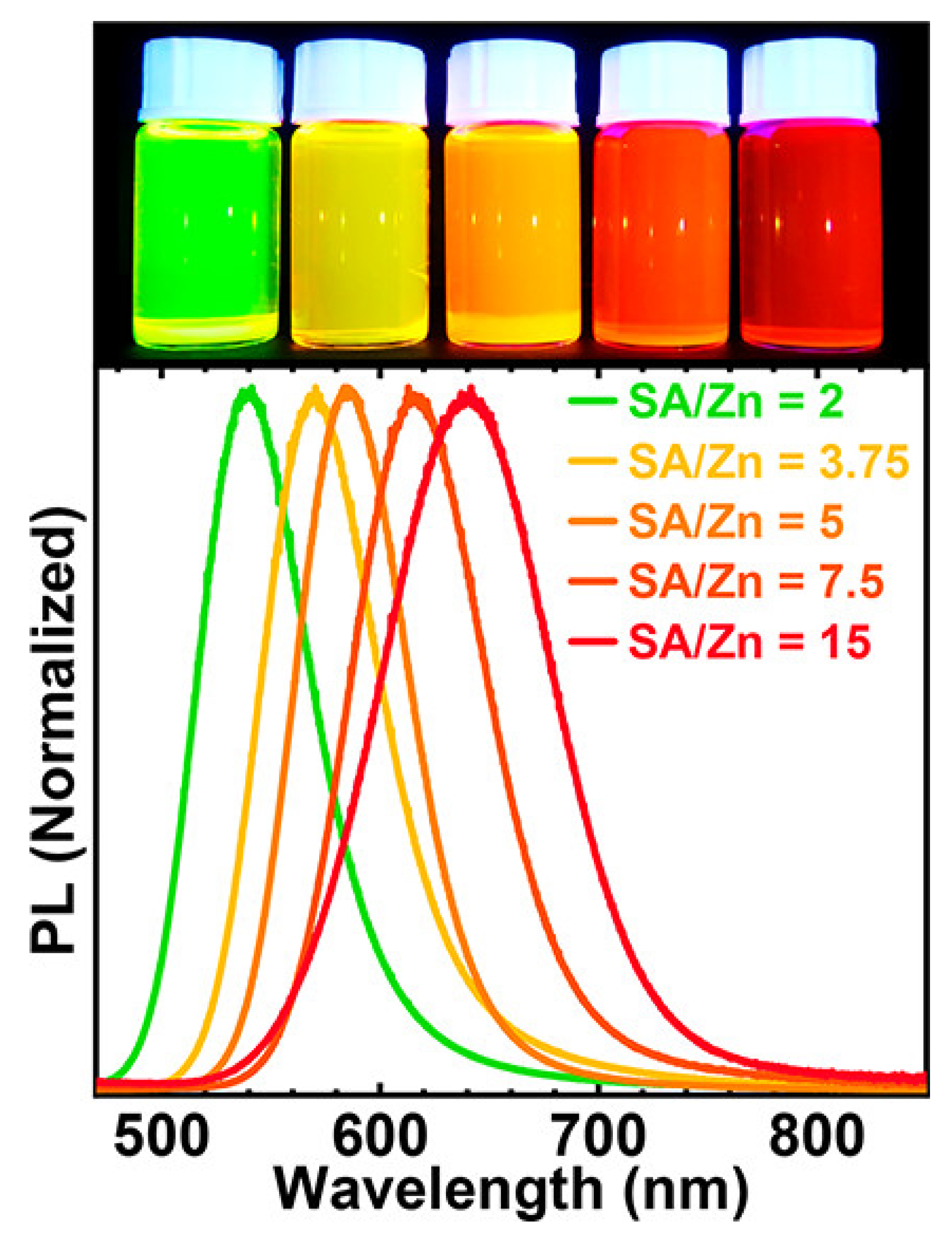
2.2. Quantum Dot-Based Nuclear Sensors

Quantum dots (QDs) are semiconductor nanocrystals with typical diameters between 2 and 10 nm that confine charge carriers in all three spatial dimensions. This quantum confinement produces discrete energy levels, in contrast to the continuous bands observed in bulk materials, and enables precise tuning of the optical and electronic properties [28]. For example, a decrease in the QD diameter increases the band gap, resulting in a shift of the photoluminescence emission towards the blue end of the spectrum, while larger dots emit at longer (red) wavelengths [29,30]. This tunability is critical for radiation detection, as it allows QDs to be engineered to emit at wavelengths that correspond to specific energy signatures of ionizing radiation [31].
When QDs are exposed to high-energy particles (e.g., gamma rays, X-rays, or alpha particles), excitons are generated as electrons are promoted to higher energy states [29]. The radiative recombination of these electron–hole pairs yields photons with energies characteristic of the QD’s band gap [30]. This can be seen in the photoluminescence spectra of various QDs in Figure 2. The resulting narrow emission spectra, with full widths at half maximum typically in the 20–30 nm range, enable fine discrimination between different radiation energies [32]. This high energy resolution is very important for identifying and quantifying specific radioactive isotopes in applications such as reactor monitoring and waste management [31,33].
The synthesis of quantum dots is achieved primarily by colloidal methods [35] and, to a lesser extent, by molecular beam epitaxy (MBE) [36]. Colloidal synthesis involves the thermal decomposition of organometallic precursors in the presence of surfactants, which control nucleation and growth to yield QDs with relatively narrow size distributions [35]. Although this method is scalable and cost-effective, variations in particle size cause non-uniform optical responses [37]. MBE, while offering improved control over QD size and composition, is more complex and expensive, making it less amenable to large-scale production [37,38]. Advances in synthesis protocols aim to improve yield and uniformity while reducing production costs.
In sensor applications, QDs are typically integrated into hybrid device architectures. For instance, QDs may be embedded within a polymer matrix [39] or coupled with conventional semiconductor detectors [40]. In these devices, the QD ensemble absorbs ionizing radiation, and the subsequent emission is collected by a photodetector system. The intensity and spectral characteristics of the emitted light are then correlated with the radiation dose and energy spectrum [32]. This approach allows for the development of compact, high-density sensor arrays capable of spatially resolved radiation mapping—a feature that is particularly beneficial for both fixed installations and portable, wearable radiation monitors [28,41,42].
While QDs generally maintain their structural and optical properties under moderate radiation doses, extended exposure can lead to degradation of the surface passivation layer, resulting in photobleaching and reduced sensitivity [43,44]. To address these difficulties, advancements are being made towards enhancing the radiation hardness of QDs via improved surface chemistry, such as robust encapsulation techniques and the use of protective coatings that mitigate oxidation and other degradation pathways [45,46,47].

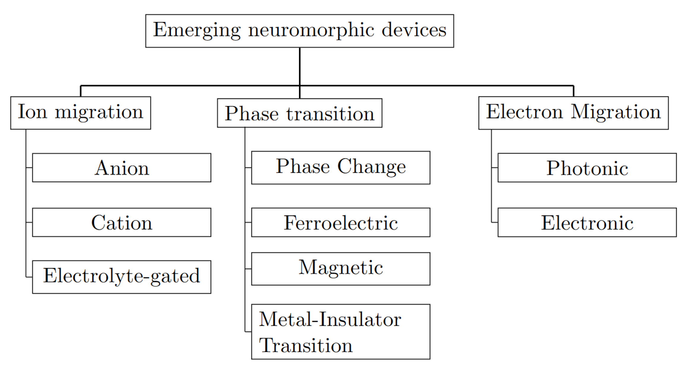
2.3. Neuromorphic Nuclear Sensors

Neuromorphic devices are a class of hardware systems designed to replicate the functional principles of biological neural networks. Neuromorphic devices aim to emulate the brain’s efficiency in processing, learning, and adapting to complex stimuli [48].
A central element in many neuromorphic systems is the memristor, a device whose resistance can be modified by the history of electrical activity. Memristive devices are typically fabricated using thin films of metal oxides, such as hafnium oxide (HfO2), deposited via atomic layer deposition (ALD) [49]. In these devices, precise control over film thickness and stoichiometry is achieved by adjusting ALD parameters [50]. Electrical measurements on memristors reveal distinct switching behavior: the devices transition between high-resistance and low-resistance states when a voltage within the range of 0.8–1.2 V is applied [51]. In fact, these devices can switch reliably for over 10 4 cycles.
Two-terminal memristors, phase-change materials (PCMs), and three-terminal devices such as electrochemical transistors and ferroelectric transistors are central to neuromorphic designs [52]. This review will touch only on these types of neuromorphic devices, but there are many other types, as seen in Figure 3.
Phase-change materials (PCMs) such as Ge2Sb2Te5 (GST) provide an alternative mechanism for storing analog information, especially in optoeletronics [53]. Unlike memristors, which change resistance through ion migration or filament formation, PCMs rely on the reversible phase transition between amorphous and crystalline states [51,54]. GST films are deposited using techniques such as molecular beam epitaxy (MBE) [55] or sputtering [56], followed by a carefully controlled thermal annealing process that induces the phase change [57]. Measurements using time-resolved electrical characterization show that the transition occurs within approximately 10 ns. The PCM devices are capable of exhibiting multiple discrete conductance levels, a property confirmed by constructing conductance histograms from current/voltage data [58].
Spiking neural network (SNN) architectures are employed to process the output from these devices. In an SNN, the sensor output is represented by voltage spikes that occur when the input radiation exceeds a defined threshold [59]. The networks incorporate spike-timing-dependent plasticity (STDP) rules, a learning mechanism in which the temporal correlation between spikes adjusts the effective synaptic weights.
The fabrication of neuromorphic sensor arrays involves advanced lithographic techniques. Electron-beam lithography is commonly used to define patterns for memristors and PCM cells with feature sizes on the order of nanometers [60]. Subsequent processing steps, such as plasma etching [61] and chemical mechanical polishing, are optimized to ensure uniformity across large device areas. Flexible substrates have been employed to demonstrate that neuromorphic sensor arrays can be integrated into conformable platforms [62]. This integration is particularly important for applications in portable radiation detection or wearable safety devices that can be used in emergency response scenarios.
Neuromorphic devices have been exposed to gamma radiation from Co-60 sources, with cumulative doses reaching 5–10 kGy [63]. Electrical characterization performed before and after irradiation indicates that the threshold voltages and switching dynamics of both memristors and PCMs remain stable [64].

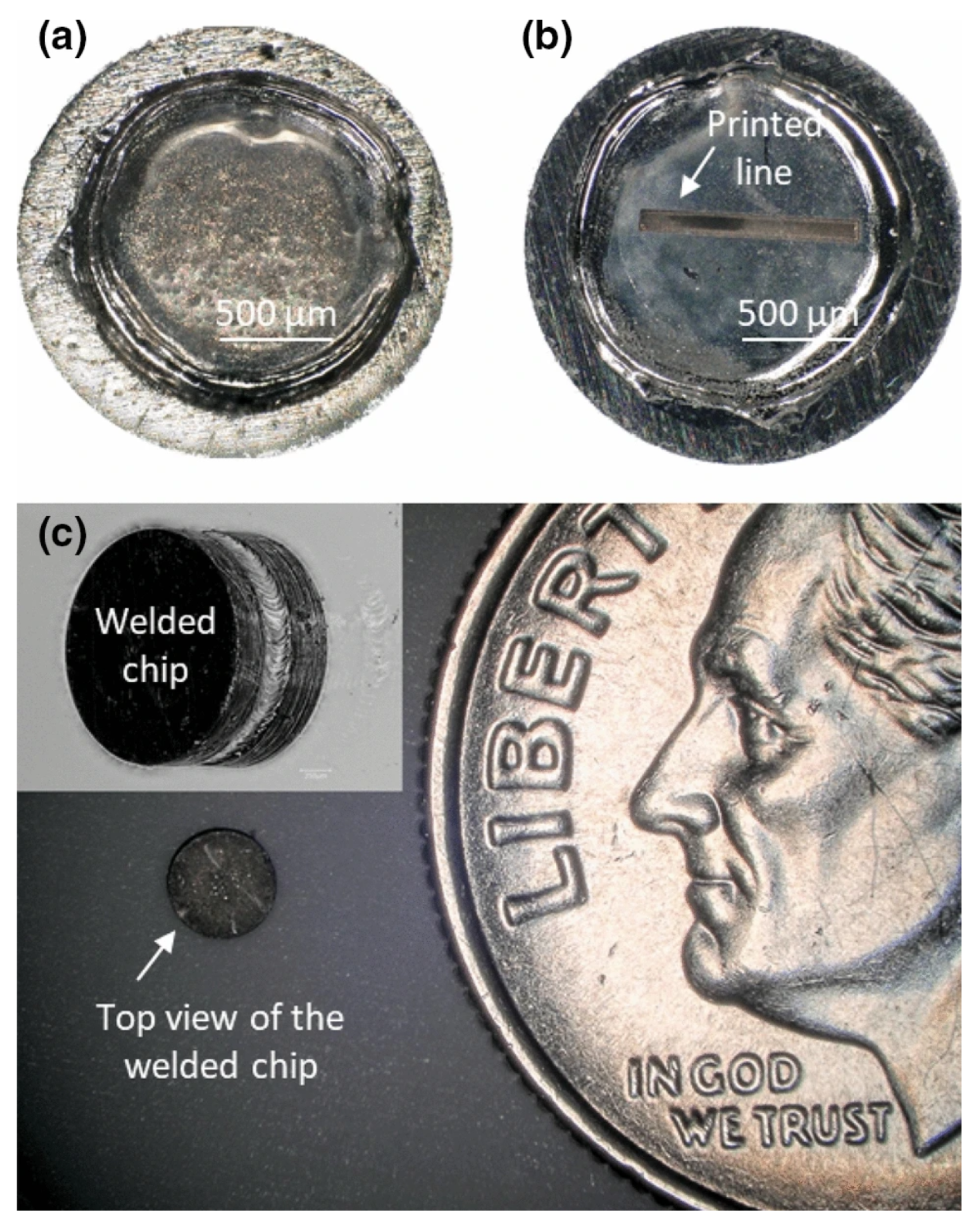
2.4. Solid-State Nuclear Sensors

Solid-state nuclear sensors based on metal oxide semiconductors have become a promising approach for detecting ionizing radiation. Materials such as zinc oxide (ZnO), tin oxide (SnO2), and titanium dioxide (TiO2) are widely used (e.g., [65,66,67]) because of their well-defined semiconducting properties and inherent material stability.
In these sensors, the fundamental mechanism relies on the interaction of ionizing radiation with the metal oxide, which generates electron–hole pairs [68]. This generation of charge carriers leads to a measurable increase in conductivity. For example, when radiation excites electrons from the valence band into the conduction band, the resulting change in carrier density is directly correlated with the intensity and energy of the incident radiation [69].
One of the key advantages of metal oxide sensors is their robustness and stability in harsh environments. Metal oxides are known for their chemical and thermal stability, making them suitable for applications in extreme conditions, such as high-temperature zones within nuclear reactors [70,71,72]. Metal oxide semiconductors have been used in wearable sensor applications, and show great potential for nuclear sensing applications [73].
Metal oxide nuclear sensors have found applications across several domains. In NPPs, metal oxide sensors contribute to the safety and efficiency of reactor operations by monitoring neutron and gamma radiation levels [74]. Metal oxide sensors also exhibit sensitivity to low levels of radiation. In environmental monitoring, this property is extremely valuable for detecting radioactive contaminants in air, water, and soil [75]. In medical imaging, metal oxide sensors are being explored for their potential to improve the detection capabilities of imaging equipment [7,76].
Integration with advanced technologies is opening new avenues for metal oxide nuclear sensors. The combination of these sensors with wireless communication systems enables remote monitoring of radiation levels in inaccessible or hazardous areas [77]. Moreover, incorporating artificial intelligence and machine learning algorithms allows for sophisticated data analysis, improving the interpretation of sensor data and predictive capabilities [78].

3. Applications of Nuclear Sensors

3.1. Nuclear Power Plant Safety

Nuclear sensors have a wide array of applications. In NPPs, nuclear sensors are invaluable for measuring the levels of radiation inside and outside the nuclear power plant. Without nuclear sensors, the safety of the workers and environment would be largely uncertain. Nuclear sensors can detect leaks in the reactor coolant system, measure the amount of radioactive material released into the environment, and monitor the levels of radiation of spent nuclear fuel in waste storage environments.

3.2. Medical Imaging

In medical imaging, techniques like Positron Emission Tomography (PET) and Single-Photon Emission Computed Tomography (SPECT) require incredibly sensitive, accurate, and fast radiation detectors [79,80]. Advanced sensor technologies can improve SPECT imaging by improving both spatial resolution and energy discrimination. For example, graphene-based sensors, with their extraordinary intrinsic electron mobility (often exceeding 200 , 000 c m 2 /Vs in optimized CVD-grown monolayers [9]) and exceptional thermal conductivity (up to 5000 W/mK [16]), provide rapid charge collection and high sensitivity to gamma photons. Graphene’s atomic-scale thickness and large specific surface area (approximately 2630 m 2 /g) facilitate efficient interactions with gamma emissions in the 70–300 keV energy range [81]. However, sustained exposure to ionizing radiation (e.g., cumulative doses in the range of 1–2 kGy) may induce defect formation [82]. This is evidenced by an increased I D / I G ratio in the Raman spectra [83].

3.3. Environmental Monitoring

The detection and monitoring of toxic compounds in the air, water, and soil proves to be an ongoing challenge for environmental scientists. Not only can nuclear sensors help prevent radiation exposure of humans and wildlife from reaching a harmful level but they show great promise in detecting the toxic compounds in the air, water, and soil [8]. The advancement of nuclear sensor technology improves the detection of unwanted compounds in the air, water, and soil, thereby improving the safety and health of humans and wildlife.

4. Challenges and Future Directions

The large-scale implementation of nuclear sensor technology shows great promise in domains such as NPPs, medical imaging, and environmental monitoring. However, despite the usefulness of these sensors, there are many challenges that need to be addressed.

4.1. Fabrication Costs

The fabrication cost of graphene is approximately USD 1–2 per c m 2 [84]. The market cost, however, is much higher, often reaching USD 10–20 per c m 2 on the graphene supermarket. In comparison, quantum dot synthesis through colloidal methods typically ranges from USD 11 to 73 per g of material [85], although achieving a uniform particle size distribution remains a technical challenge [86]. Neuromorphic sensor components, particularly memristive devices produced via atomic layer deposition (ALD), demand advanced deposition systems and precision lithography [87], leading to quickly intractable estimates for cost of production [88].

4.2. Sensor Size

The physical dimensions of nuclear sensors play a critical role in their integration into environments limited in space, like nuclear power plants and security installations. Traditional sensor systems typically include not only sensitive elements but also supporting circuitry, packaging, and thermal management components, which together can result in a bulky overall design. Recent advancements in micro- and nano-fabrication techniques [89] have enabled the development of sensor elements with dimensions on the order of micrometers [90]. For example, printed electronics and flexible substrates have been used to fabricate sensor arrays with significantly reduced footprints [91], while system-in-package (SiP) [92] and wafer-level packaging [93] approaches further minimize the overall size of the sensor module. These miniaturization strategies improve the ability to integrate sensors into existing systems without requiring substantial modifications. Compact sensor designs not only address environments with limited space but also enhance system integration and potentially lower material and assembly costs through scalable manufacturing processes.

4.3. Sensor Sensitivity

The sensitivity of nuclear sensors is paramount for detecting trace levels of radiation; however, achieving a balance between high sensitivity and low false alarm rates remains a significant challenge. Sensors must reliably detect low-intensity ionizing radiation (e.g., detection limits below 0.1 µGy/h in environmental monitoring [94]) while avoiding spurious responses to background noise or non-hazardous stimuli. This balance is often quantified by the sensor’s signal-to-noise ratio (SNR) and detection threshold. For instance, a sensor designed for nuclear power plant monitoring must achieve a high SNR to discern minute changes in radiation levels yet incorporate efficient signal discrimination algorithms—such as adaptive filtering [95] machine learning [96,97] techniques—to prevent false-positive detections that could lead to unnecessary operational disruptions or safety risks.

4.4. Advanced Manufacturing and Integration Techniques

Advances in the manufacturing techniques used to create nuclear sensors are critical for developing compact, scalable, and cost-effective nuclear sensors. Recent work has focused on innovative fabrication methods, such as the use of printed melt wire chips for temperature sensing in nuclear reactors. For instance, melt wire chips—fabricated by printing silver melt wires onto grooved steel substrates—demonstrate sensor dimensions as small as 2 mm (see Figure 4) [2], which is particularly advantageous for environments with limited space, such as nuclear power plants.
Techniques like roll-to-roll printing [37,98], microfabrication [99], and additive manufacturing [2,3,4] are being optimized to produce high-performance sensor components at a reduced cost and with enhanced reproducibility. These methods help in minimizing the overall size and weight of the sensors. As manufacturing processes continue to mature, the combined effect of material innovations and advanced fabrication will drive the widespread deployment of nuclear sensor technologies, making them more accessible, reliable, and effective in a wide range of applications.

5. Conclusions

Nuclear sensor technologies have evolved significantly in recent years, providing a range of benefits in various fields, including NPPs, medical imaging, and environmental monitoring. This review has highlighted the recent advancements in nuclear sensor technologies, including the use of new materials and technologies to improve the performance of these sensors. Despite the progress made, there are still challenges that need to be addressed, such as cost, size, and sensitivity. Researchers need to continue exploring new ways to reduce the cost of these sensors, develop smaller and more compact sensors, and improve their sensitivity to ensure they are reliable and effective in various applications. Looking towards the future, the potential impact of advancements in nuclear sensor technologies is significant, and they have the potential to further improve safety in nuclear power plants, enhance medical imaging, and improve environmental monitoring.

Author Contributions

Conceptualization, K.M. and J.H.; investigation, J.H.; writing—original draft preparation, J.H.; writing—review and editing, J.H., K.M. and O.M.; supervision, K.M.; project administration, O.M.; funding acquisition, K.M. All authors have read and agreed to the published version of the manuscript.

Funding

This work was supported in part by the U.S. Department of Energy, Office of Science, Office of Workforce Development for Teachers and Scientists (WDTS) under the Science Undergraduate Laboratory Internships (SULI) program.

Data Availability Statement

No new data were created or analyzed in this study.

Acknowledgments

This manuscript has been authored by UT-Battelle LLC under contract DE-AC05-00OR22725 with the US Department of Energy (DOE). The publisher, by accepting the article for publication, acknowledges that the US government retains a nonexclusive, paid-up, irrevocable, worldwide license to publish or reproduce the published form of this manuscript, or allow others to do so, for US government purposes. DOE will provide public access to these results of federally sponsored research in accordance with the DOE Public Access Plan (https://www.energy.gov/doe-public-access-plan) (accessed on 1 January 2025). The authors gratefully acknowledge the support of the ORNL Nuclear Energy and Fuel Cycle Division.

Conflicts of Interest

The authors declare no conflicts of interest.

References

  1. Shubayr, N. Nuclear security measures: A review of selected emerging technologies and strategies. J. Radiat. Res. Appl. Sci. 2024, 17, 100814. [Google Scholar] [CrossRef]
  2. Mondal, K.; Fujimoto, K.; McMurtrey, M.D. Advanced Manufacturing of Printed Melt Wire Chips for Cheap, Compact Passive In-Pile Temperature Sensors. JOM 2020, 72, 4196–4201. [Google Scholar] [CrossRef]
  3. McMurtrey, M.; Mondal, K.; Fujimoto, K.; Bass, J.; Biaggne, A. Report on Plasma Jet Printer for Sensor Fabrication with Process Parameters Optimized by Simulation Input; U.S. Department of Energy Office of Nuclear Energy: Washington, DC, USA, 2019. [CrossRef]
  4. Wilding, M.; Mondal, K.; Lloyd, R.; Fujimoto, K.; McMurtrey, M.; Unruh, T. Initial Temperature Testing of Advanced Manufactured Melt Wire Package; U.S. Department of Energy National Laboratory: Pittsburgh, PA, USA, 2020. [CrossRef]
  5. Daw, J.; Unruh, T.C.; Heidrich, B.J.; Hurley, D.H.; Fujimoto, K.T.; Estrada, D.; McMurtrey, M.; Mondal, K.; Hone, L.; Seifert, R.D.; et al. Sensors for Passively Measuring a Maximum Temperature of a Nuclear Reactor, and Related Methods. U.S. Patent 11,923,097, 5 March 2024. [Google Scholar]
  6. Kim, K.C.; Kwon, H.K.; Park, J.S.; Seong, U.H. Evaluation of Dynamic J-R Curve for Leak Before Break Design of Nuclear Reactor Coolant Piping System; IntechOpen: London, UK, 2011. [Google Scholar]
  7. Michail, C.; Liaparinos, P.; Kalyvas, N.; Kandarakis, I.; Fountos, G.; Valais, I. Radiation Detectors and Sensors in Medical Imaging. Sensors 2024, 24, 6251. [Google Scholar] [CrossRef] [PubMed]
  8. Khizar, S.; Zine, N.; Jaffrezic-Renault, N.; Elaissari, A.; Errachid, A. Prospective analytical role of sensors for environmental screening and monitoring. TrAC Trends Anal. Chem. 2022, 157, 116751. [Google Scholar] [CrossRef]
  9. Bolotin, K.I.; Sikes, K.; Jiang, Z.; Klima, M.; Fudenberg, G.; Hone, J.; Kim, P.; Stormer, H.L. Ultrahigh electron mobility in suspended graphene. Solid State Commun. 2008, 146, 351–355. [Google Scholar] [CrossRef]
  10. Mir, S.H.; Yadav, V.K.; Singh, J.K. Recent Advances in the Carrier Mobility of Two-Dimensional Materials: A Theoretical Perspective. ACS Omega 2020, 5, 14203–14211. [Google Scholar] [CrossRef]
  11. Urade, A.R.; Lahiri, I.; Suresh, K.S. Graphene properties, synthesis and applications: A review. JOM 2023, 75, 614–630. [Google Scholar] [CrossRef]
  12. Fuad, M.H.; Nayan, M.F.; Raihan, M.A.; Yeassin, R.; Mahmud, R.R. Performance analysis of graphene field effect transistor at nanoscale regime. e-Prime—Adv. Electr. Eng. Electron. Energy 2024, 9, 100679. [Google Scholar] [CrossRef]
  13. Yan, Q.L.; Gozin, M.; Zhao, F.Q.; Cohen, A.; Pang, S.P. Highly energetic compositions based on functionalized carbon nanomaterials. Nanoscale 2016, 8, 4799–4851. [Google Scholar] [CrossRef]
  14. Warda, M.; Badih, K. Graphene Field Effect Transistors: A Review. arXiv 2021, arXiv:2010.10382v2. [Google Scholar]
  15. Jovanovic, I.; Koybasi, O.; Cazalas, E.; Childres, I.; Chen, Y. Performance and Design Optimization of Graphene Field-Effect Transistors for Radiation Detection. Trans. Am. Nucl. Soc. 2013, 108, 259–260. [Google Scholar]
  16. Balandin, A.A.; Ghosh, S.; Bao, W.; Calizo, I.; Teweldebrhan, D.; Miao, F.; Lau, C.N. Superior thermal conductivity of single-layer graphene. Nano Lett. 2008, 8, 902–907. [Google Scholar] [CrossRef] [PubMed]
  17. Memarian, F.; Fereidoon, A.; Darvish Ganji, M. Graphene Young’s modulus: Molecular mechanics and DFT treatments. Superlattices Microstruct. 2015, 85, 348–356. [Google Scholar] [CrossRef]
  18. Sun, L.; Yuan, G.; Gao, L.; Yang, J.; Chhowalla, M.; Gharahcheshmeh, M.H.; Gleason, K.K.; Choi, Y.S.; Hong, B.H.; Liu, Z. Chemical vapour deposition. Nat. Rev. Methods Prim. 2021, 1, 5. [Google Scholar] [CrossRef]
  19. Saeed, M.; Alshammari, Y.; Majeed, S.A.; Al-Nasrallah, E. Chemical vapour deposition of graphene-synthesis, characterisation, and applications: A review. Molecules 2020, 25, 3856. [Google Scholar] [CrossRef]
  20. Pham, P.V.; Mai, T.H.; Dash, S.P.; Biju, V.; Chueh, Y.L.; Jariwala, D.; Tung, V. Transfer of 2D Films: From Imperfection to Perfection. ACS Nano 2024, 18, 14841–14876. [Google Scholar] [CrossRef]
  21. Liu, N.; Pan, Z.; Fu, L.; Zhang, C.; Dai, B.; Liu, Z. The origin of wrinkles on transferred graphene. Nano Res. 2011, 4, 996–1004. [Google Scholar] [CrossRef]
  22. Suzuki, S.; Orofeo, C.M.; Wang, S.; Maeda, F.; Takamura, M.; Hibino, H. Structural instability of transferred graphene grown by chemical vapor deposition against heating. J. Phys. Chem. C 2013, 117, 22123–22130. [Google Scholar] [CrossRef]
  23. Li, X.; Zhu, Y.; Cai, W.; Borysiak, M.; Han, B.; Chen, D.; Piner, R.D.; Colombo, L.; Ruoff, R.S. Transfer of large-area graphene films for high-performance transparent conductive electrodes. Nano Lett. 2009, 9, 4359–4363. [Google Scholar] [CrossRef]
  24. Suk, J.W.; Lee, W.H.; Lee, J.; Chou, H.; Piner, R.D.; Hao, Y.; Akinwande, D.; Ruoff, R.S. Enhancement of the electrical properties of graphene grown by chemical vapor deposition via controlling the effects of polymer residue. Nano Lett. 2013, 13, 1462–1467. [Google Scholar] [CrossRef]
  25. Li, N.; Zhen, Z.; Zhang, R.; Xu, Z.; Zheng, Z.; He, L. Nucleation and growth dynamics of graphene grown by radio frequency plasma-enhanced chemical vapor deposition. Sci. Rep. 2021, 11, 6007. [Google Scholar] [CrossRef] [PubMed]
  26. Yazdi, G.R.; Iakimov, T.; Yakimova, R. Epitaxial Graphene on SiC: A Review of Growth and Characterization. Crystals 2016, 6, 53. [Google Scholar] [CrossRef]
  27. Jia, Y.; Sun, X.; Shi, Z.; Jiang, K.; Wu, T.; Liang, H.; Cui, X.; Lü, W.; Li, D. Improved performance of SiC radiation detectors due to optimized ohmic contact electrode by graphene insertion. Diam. Relat. Mater. 2021, 115, 108355. [Google Scholar] [CrossRef]
  28. Torimoto, T.; Kameyama, T.; Uematsu, T.; Kuwabata, S. Controlling optical properties and electronic energy structure of I–III–VI semiconductor quantum dots for improving their photofunctions. J. Photochem. Photobiol. C Photochem. Rev. 2023, 54, 100569. [Google Scholar] [CrossRef]
  29. Leong, K.H.; Chin, Y.H.; Sim, L.C.; Tan, B.; Dai, C.; Saravanan, P. Physical properties of quantum dots. In Graphene, Nanotubes and Quantum Dots-Based Nanotechnology; Elsevier: Amsterdam, The Netherlands, 2022; pp. 687–709. [Google Scholar] [CrossRef]
  30. Sanmartín-Matalobos, J.; Bermejo-Barrera, P.; Aboal-Somoza, M.; Fondo, M.; García-Deibe, A.M.; Corredoira-Vázquez, J.; Alves-Iglesias, Y. Semiconductor Quantum Dots as target analytes: Properties, surface chemistry and detection. Nanomaterials 2022, 12, 2501. [Google Scholar] [CrossRef]
  31. Williams, R.T.; Wolszczak, W.W.; Yan, X.; Carroll, D.L. Perovskite Quantum-Dot-in-Host for Detection of Ionizing Radiation. ACS Nano 2020, 14, 5161–5169. [Google Scholar] [CrossRef]
  32. Mangnus, M.J.J.; de Wit, J.W.; Vonk, S.J.W.; Geuchies, J.J.; Albrecht, W.; Bals, S.; Houtepen, A.J.; Rabouw, F.T. High-Throughput Characterization of Single-Quantum-Dot Emission Spectra and Spectral Diffusion by Multiparticle Spectroscopy. ACS Photonics 2023, 10, 2688–2698. [Google Scholar] [CrossRef]
  33. Brus, L.E. Electron–electron and electron-hole interactions in small semiconductor crystallites: The size dependence of the lowest excited electronic state. J. Chem. Phys. 1984, 80, 4403–4409. [Google Scholar] [CrossRef]
  34. Darwan, D.; Lim, L.J.; Wang, T.; Wijaya, H.; Tan, Z.K. Ultra-Confined Visible-Light-Emitting Colloidal Indium Arsenide Quantum Dots. Nano Lett. 2021, 21, 5167–5172. [Google Scholar] [CrossRef]
  35. Paredes, I.J.; Sahu, A. Synthesis and Structure of Colloidal Quantum Dots; American Chemical Society: Washington, DC, USA, 2023. [Google Scholar] [CrossRef]
  36. Franchi, S.; Trevisi, G.; Seravalli, L.; Frigeri, P. Quantum dot nanostructures and molecular beam epitaxy. Prog. Cryst. Growth Charact. Mater. 2003, 47, 166–195. [Google Scholar] [CrossRef]
  37. Ma, Y.F.; Wang, Y.M.; Wen, J.; Li, A.; Li, X.L.; Leng, M.; Zhao, Y.B.; Lu, Z.H. Review of roll-to-roll fabrication techniques for colloidal quantum dot solar cells. J. Electron. Sci. Technol. 2023, 21, 100189. [Google Scholar] [CrossRef]
  38. Balazs, D.M.; Loi, M.A. Lead-Chalcogenide Colloidal-Quantum-Dot Solids: Novel Assembly Methods, Electronic Structure Control, and Application Prospects. Adv. Mater. 2018, 30, 1800082. [Google Scholar] [CrossRef]
  39. Sosna-Głębska, A.; Rezek, B.; Ukraintsev, E.; Sibiński, M. Perovskite QDs embedded in polymer as a wavelength-shifting layer for UV-sensitized silicon sensors. J. Lumin. 2024, 272, 120618. [Google Scholar] [CrossRef]
  40. Cotta, M.A. Quantum Dots and Their Applications: What Lies Ahead? ACS Appl. Nano Mater. 2020, 3, 4920–4924. [Google Scholar] [CrossRef]
  41. Kagan, C.R.; Lifshitz, E.; Sargent, E.H.; Talapin, D.V. Building devices from colloidal quantum dots. Science 2016, 353, aac5523. [Google Scholar] [CrossRef] [PubMed]
  42. Lee, K.S.; Shim, J.; Park, M.; Kim, H.Y.; Son, D.I. Transparent nanofiber textiles with intercalated ZnO@graphene QD LEDs for wearable electronics. Compos. Part B Eng. 2017, 130, 70–75. [Google Scholar] [CrossRef]
  43. He, Z.; Xie, T.; Yu, H.; Ge, J.; Dai, W. Evaluation of quantum dot composite graphene /Titanium oxide enhanced UV aging resistance modified asphalt. Constr. Build. Mater. 2023, 408, 133732. [Google Scholar] [CrossRef]
  44. Fedoseyev, A.I.; Turowski, M.; Raman, A.; Taylor, E.W.; Hubbard, S.; Polly, S.; Shao, Q.; Balandin, A.A. Space radiation effects modeling and analysis of quantum dot based photovoltaic cells. In Proceedings of the Nanophotonics and Macrophotonics for Space Environments III, San Diego, CA, USA, 3–4 August 2009; Taylor, E.W., Cardimona, D.A., Eds.; SPIE: Bellingham, WA, USA, 2009; Volume 7467, p. 746705. [Google Scholar] [CrossRef]
  45. Giroux, M.; Zahra, Z.; Salawu, O.A.; Burgess, R.M.; Ho, K.T.; Adeleye, A.S. Assessing the environmental effects related to quantum dot structure, function, synthesis and exposure. Environ. Sci. Nano 2022, 9, 867–910. [Google Scholar]
  46. Park, J.; Yoo, G.; Heo, J. CdSe/ZnS quantum dot encapsulated MoS2 phototransistor for enhanced radiation hardness. Sci. Rep. 2019, 9, 1411. [Google Scholar] [CrossRef]
  47. Silva, M.R.; Alves, M.F.; Ananias, D.; Ivanov, M.; Fernandes, M.H.V.; Vilarinho, P.M.; Ferreira, P. Development of carbon quantum dots-based transparent coatings for enhanced UV shielding. Appl. Surf. Sci. 2024, 669, 160414. [Google Scholar] [CrossRef]
  48. Zhu, J.; Zhang, T.; Yang, Y.; Huang, R. A comprehensive review on emerging artificial neuromorphic devices. Appl. Phys. Rev. 2020, 7, 011312. [Google Scholar] [CrossRef]
  49. Briggs, B.; Bishop, S.; Leedy, K.; Cady, N. Characterization of hafnium oxide resistive memory layers deposited on copper by atomic layer deposition. Thin Solid Film. 2014, 562, 519–524. [Google Scholar] [CrossRef]
  50. Aussen, S.; Hardtdegen, A.; Dittmann, R.; Hoffmann-Eifert, S. Memristive Devices Formed By ALD Metal Oxide Growth on a Hafnium Layer – Study of the Interfacial HfO2 Formation. ECS Meet. Abstr. 2019, MA2019-02, 1232. [Google Scholar] [CrossRef]
  51. Hellenbrand, M.; MacManus-Driscoll, J. Multi-level resistive switching in hafnium-oxide-based devices for neuromorphic computing. Nano Converg. 2023, 10, 44. [Google Scholar] [CrossRef] [PubMed]
  52. Kim, M.K.; Park, Y.; Kim, I.J.; Lee, J.S. Emerging Materials for Neuromorphic Devices and Systems. iScience 2020, 23, 101846. [Google Scholar] [CrossRef] [PubMed]
  53. Sahoo, D.; Naik, R. GSST phase change materials and its utilization in optoelectronic devices: A review. Mater. Res. Bull. 2022, 148, 111679. [Google Scholar] [CrossRef]
  54. Wełnic, W.; Wuttig, M. Reversible switching in phase-change materials. Mater. Today 2008, 11, 20–27. [Google Scholar] [CrossRef]
  55. Shayduk, R.; Braun, W. Epitaxial films for Ge–Sb–Te phase change memory. J. Cryst. Growth 2009, 311, 2215–2219. [Google Scholar] [CrossRef]
  56. Prili, S.; Bragaglia, V.; Jonnalagadda, V.P.; Luchtenveld, J.; Arciprete, F.; Kooi, B.J.; Sebastian, A.; Syed, G.S. Understanding the Growth and Properties of Sputter-Deposited Phase-Change Superlattice Films. arXiv 2025, arXiv:2303.10780v2. [Google Scholar]
  57. Javanbakht, M.; Mohebbi, S.; Attariani, H. Stress Engineering: The Response of Phase Change Materials to Mechanical Stimuli. ACS Appl. Electron. Mater. 2023, 5, 3521–3530. [Google Scholar]
  58. Liu, C.; Qian, R.; Liu, Z.; Liu, G.; Zhang, Y. Multi-scale modelling of thermal conductivity of phase change material/recycled cement paste incorporated cement-based composite material. Mater. Des. 2020, 191, 108646. [Google Scholar] [CrossRef]
  59. Malcolm, K.; Casco-Rodriguez, J. A Comprehensive Review of Spiking Neural Networks: Interpretation, Optimization, Efficiency, and Best Practices. arXiv 2023, arXiv:2303.10780v2. [Google Scholar]
  60. Keser, Y.I.; Saka Yıldırım, K.; Gökcen, D. Patterning Titanium Dioxide Based Memristors Using Electron Beam Lithography. In Proceedings of the 2020 International Congress on Human-Computer Interaction, Optimization and Robotic Applications (HORA), Ankara, Turkey, 26–28 June 2020; pp. 1–8. [Google Scholar] [CrossRef]
  61. Saludes-Tapia, M.; Campabadal, F.; Miranda, E.; González, M. Impact of the W etching process on the resistive switching properties of TiN/Ti/HfO2/W memristors. Solid-State Electron. 2023, 207, 108718. [Google Scholar] [CrossRef]
  62. Wang, H.; Sun, B.; Ge, S.S.; Su, J.; Jin, M.L. On non-von Neumann flexible neuromorphic vision sensors. npj Flex. Electron. 2024, 8, 28. [Google Scholar] [CrossRef]
  63. Pattnaik, D.P.; Andrews, C.; Cropper, M.D.; Gabbitas, A.; Balanov, A.G.; Savel’ev, S.; Borisov, P. Gamma radiation-induced nanodefects in diffusive memristors and artificial neurons. Nanoscale 2023, 15, 15665–15674. [Google Scholar] [CrossRef]
  64. Pattnaik, D.P.; Andrews, C.; Cropper, M.D.; Balanov, A.; Saveliev, S.; Borisov, P. Effect of gamma radiation on electrical properties of diffusive memristor devices. arXiv 2023, arXiv:2303.12762v1. [Google Scholar]
  65. Sahani, R.; Dixit, A. A comprehensive review on zinc oxide bulk and nano-structured materials for ionizing radiation detection and measurement applications. Mater. Sci. Semicond. Process. 2022, 151, 107040. [Google Scholar] [CrossRef]
  66. Zhang, J.-C.; Shen, J.Q.; Shan, Z.-J.; Zhou, S.-X.; Zhu, J.-J. Radiation effects in tin dioxide as gas sensors. Nucl. Instruments Methods Phys. Res. Sect. B Beam Interact. Mater. Atoms 1994, 91, 663–666. [Google Scholar] [CrossRef]
  67. Ghamarpoor, R.; Fallah, A.; Jamshidi, M. Investigating the use of titanium dioxide (TiO2) nanoparticles on the amount of protection against UV irradiation. Sci. Rep. 2023, 13, 9793. [Google Scholar] [CrossRef]
  68. Dey, A. Semiconductor metal oxide gas sensors: A review. Mater. Sci. Eng. B 2018, 229, 206–217. [Google Scholar] [CrossRef]
  69. Hahn, G.; Joos, S. State-of-the-Art Industrial Crystalline Silicon Solar Cells. In Advances in Photovoltaics: Part 3; Elsevier: Amsterdam, The Netherlands, 2014; pp. 1–72. [Google Scholar] [CrossRef]
  70. Jia, B.; Xu, W.; Li, J.; Liu, X.; Ji, L.; Sun, C.; Li, J.; Li, H. Enhancement of thermal stability and high-temperature oxidation resistance of chromium oxide-based films by addition of rare earth element Y. J. Mater. Sci. Technol. 2024, 188, 105–115. [Google Scholar] [CrossRef]
  71. Duncan, M.A.; Barney, L.; Dias, M.R.S.; Leite, M.S. Refractory Metals and Oxides for High-Temperature Structural Color Filters. ACS Appl. Mater. Interfaces 2022, 14, 55745–55752. [Google Scholar] [CrossRef]
  72. Su, R.; Becker, J.R.; Liu, L.; Zhang, H.; Hu, X.; Perepezko, J.H. Phase Stability During High-Temperature Oxidation. JOM 2023, 75, 4636–4643. [Google Scholar] [CrossRef]
  73. Shiiki, Y.; Nagata, S.; Takahashi, T.; Yanagida, T.; Ishikuro, H. Compact model of a metal oxide molecule sensor for self-heating control. Solid-State Electron. 2023, 204, 108641. [Google Scholar] [CrossRef]
  74. Patel, S.; Sutaria, S.; Daga, R.; Shah, M.; Prajapati, M. A systematic study on complementary metal-oxide semiconductor technology (CMOS) and Internet of Things (IOT) for radioactive leakage detection in nuclear plant. Nucl. Anal. 2023, 2, 100080. [Google Scholar] [CrossRef]
  75. Tereshkov, M.; Dontsova, T.; Saruhan, B.; Krüger, S. Metal Oxide-Based Sensors for Ecological Monitoring: Progress and Perspectives. Chemosensors 2024, 12, 42. [Google Scholar] [CrossRef]
  76. Teich, S.; Al-Rawi, W.; Heima, M.; Faddoul, F.F.; Goldzweig, G.; Gutmacher, Z.; Aizenbud, D. Image quality evaluation of eight complementary metal-oxide semiconductor intraoral digital X-ray sensors. Int. Dent. J. 2016, 66, 264–271. [Google Scholar] [CrossRef]
  77. Wang, Z.; Li, P.; Feng, B.; Feng, Y.; Cheng, D.; Wei, J. Wireless Gas Sensor Based on the Mesoporous ZnO–SnO2 Heterostructure Enables Ultrasensitive and Rapid Detection of 3-Methylbutyraldehyde. ACS Sens. 2024, 9, 2585–2595. [Google Scholar] [CrossRef]
  78. Viet, N.N.; Phuoc, P.H.; Thong, L.V.; Chien, N.V.; Van Hieu, N. A comparative study of machine learning models for identifying noxious gases through thermal fingerprint measurements and MOS sensors. Sens. Actuators A Phys. 2024, 375, 115510. [Google Scholar] [CrossRef]
  79. Zatcepin, A.; Ziegler, S.I. Detectors in positron emission tomography. Z. Med. Phys. 2023, 33, 4–12. [Google Scholar] [CrossRef]
  80. Massari, R.; Mok, G.S.P. Editorial: New trends in single photon emission computed tomography (SPECT). Front. Med. 2023, 10, 1349877. [Google Scholar]
  81. Filak-Mędoń, K.; Fornalski, K.W.; Bonczyk, M.; Jakubowska, A.; Kempny, K.; Wołoszczuk, K.; Filipczak, K.; Żerańska, K.; Zdrojek, M. Graphene-based nanocomposites as gamma- and X-ray radiation shield. Sci. Rep. 2024, 14, 18998. [Google Scholar] [CrossRef]
  82. Yasein, M.; Eissa, M.; El-Fayoumi, M.; Abood, A.A.; Badawi, E.A.; Aly, A.H. Studying the effect of low doses of gamma and beta irradiations on graphene oxide samples. Radiat. Phys. Chem. 2020, 173, 108941. [Google Scholar] [CrossRef]
  83. Shlimak, I.; Butenko, A.; Kogan, E.; Kaveh, M. Irradiation-induced broadening of the Raman spectra in monolayer graphene. J. Appl. Phys. 2019, 126, 194302. [Google Scholar] [CrossRef]
  84. Bointon, T.H.; Barnes, M.D.; Russo, S.; Craciun, M.F. High quality monolayer graphene synthesized by resistive heating cold wall chemical vapor deposition. Adv. Mater. 2015, 27, 4200. [Google Scholar] [PubMed]
  85. Jean, J.; Xiao, J.; Nick, R.; Moody, N.; Nasilowski, M.; Bawendi, M.; Bulović, V. Synthesis cost dictates the commercial viability of lead sulfide and perovskite quantum dot photovoltaics. Energy Environ. Sci. 2018, 11, 2295–2305. [Google Scholar] [CrossRef]
  86. Agarwal, K.; Rai, H.; Mondal, S. Quantum dots: An overview of synthesis, properties, and applications. Mater. Res. Express 2023, 10, 062001. [Google Scholar] [CrossRef]
  87. Hao, C.; Peng, J.; Zierold, R.; Blick, R.H. Atomic Layer Deposition Films for Resistive Random-Access Memories. Adv. Mater. Technol. 2024, 9, 2301762. [Google Scholar] [CrossRef]
  88. Adam, G.C.; Khiat, A.; Prodromakis, T. Challenges hindering memristive neuromorphic hardware from going mainstream. Nat. Commun. 2018, 9, 5267. [Google Scholar] [CrossRef]
  89. Huang, F.; Zhang, J.; Chen, T.; Pan, Q.; Zhu, Z. Advancements in manufacturing and applications of multi-dimensional micro-nano materials through interface shearing. Cell Rep. Phys. Sci. 2024, 5, 102033. [Google Scholar] [CrossRef]
  90. Planillo, J.; Alves, F. Fabrication and Characterization of Micrometer Scale Graphene Structures for Large-Scale Ultra-Thin Electronics. Electronics 2022, 11, 752. [Google Scholar] [CrossRef]
  91. Martins, P.; Pereira, N.; Lima, A.C.; Garcia, A.; Mendes-Filipe, C.; Policia, R.; Correia, V.; Lanceros-Mendez, S. Advances in Printing and Electronics: From Engagement to Commitment. Adv. Funct. Mater. 2023, 33, 2213744. [Google Scholar] [CrossRef]
  92. Pendharkar, S. Smart power technologies enabling power SOC and SIP. In Proceedings of the 2016 IEEE Symposium on VLSI Technology, Honolulu, HI, USA, 14–16 June 2016; IEEE: New York, NY, USA, 2016; pp. 1–2. [Google Scholar]
  93. Hilton, A.; Temple, D.S. Wafer-level vacuum packaging of smart sensors. Sensors 2016, 16, 1819. [Google Scholar] [CrossRef] [PubMed]
  94. Lowe, D.; Roy, L.; Tabocchini, M.A.; Rühm, W.; Wakeford, R.; Woloschak, G.E.; Laurier, D. Radiation dose rate effects: What is new and what is needed? Radiat. Environ. Biophys. 2022, 61, 507–543. [Google Scholar] [CrossRef] [PubMed]
  95. Diniz, P.S.R. Fundamentals of Adaptive Filtering. In Adaptive Filtering; Springer: Boston, MA, USA, 1997; pp. 15–69. [Google Scholar] [CrossRef]
  96. Cid Vidal, X.C.; Dieste Maroñas, L.D.; Dosil Suárez, Á.D. How to Use Machine Learning to Improve the Discrimination between Signal and Background at Particle Colliders. Appl. Sci. 2021, 11, 11076. [Google Scholar] [CrossRef]
  97. Aburakhia, S.; Shami, A.; Karagiannidis, G.K. On the Intersection of Signal Processing and Machine Learning: A Use Case-Driven Analysis Approach. arXiv 2024, arXiv:2403.17181v1. [Google Scholar]
  98. Martin, C.; Zhao, Q.; Patel, A.; Velasquez, E.; Chen, D.; Li, W. A Review of Advanced Roll-to-Roll Manufacturing: System Modeling and Control. J. Manuf. Sci. Eng. 2024, 147, 041004. [Google Scholar] [CrossRef]
  99. Kalita, K.; Ghadai, R.K.; Davim, J.P. (Eds.) Microfabrication and Nanofabrication: Precision Manufacturing; De Gruyter: Berlin, Germany, 2024. [Google Scholar] [CrossRef]
Figure 1. Various carbon-based nanomaterials. Reproduced with permission from ref. [13]. Copyright 2016 Royal Society of Chemistry.
Applsci 15 02338 g001
Figure 2. UV illumination of In(Zn)As/ZnSe/ZnS QDs. From left to right, the photoluminescence (PL) and PL quantum efficiency of the QDs are as follows: 60 nm and 58% for 538 nm QD, 63 nm and 66% for 570 nm QD, 62 nm and 50% for 589 nm QD, 71 nm and 37% for 615 nm QD, and 83 nm and 15% for 635 nm QD. Reprinted (adapted) with permission from [34]. Copyright 2021 American Chemical Society.
Applsci 15 02338 g002
Figure 3. Short classification of emerging neuromorphic device technology types.
Applsci 15 02338 g003
Figure 4. (a) A blank grooved steel disk, (b) printed silver melt wire, and (c) 2 mm diameter melt wire sensor chip [2].
Applsci 15 02338 g004
Disclaimer/Publisher’s Note: The statements, opinions and data contained in all publications are solely those of the individual author(s) and contributor(s) and not of MDPI and/or the editor(s). MDPI and/or the editor(s) disclaim responsibility for any injury to people or property resulting from any ideas, methods, instructions or products referred to in the content.

