Article

Femtosecond Laser Textured Surfaces for Radiative Cooling: Black Metals

1
Optical Sciences Centre, ARC Training Centre in Surface Engineering for Advanced Materials (SEAM), Swinburne University of Technology, Hawthorn, VIC 3122, Australia
2
Quoba Systems Pty. Ltd., 26-28 Roberna St., Moorabbin, VIC 3189, Australia
3
Laser Research Center, Physics Faculty, Vilnius University, 10223 Vilnius, Lithuania
4
Department of Mechanical Engineering and Product Design Engineering, Swinburne University of Technology, Hawthorn, VIC 3122, Australia
5
Research Institute of Green Science and Technology, Shizuoka University, Hamamatsu Campus, Hamamatsu 432-8011, Japan
6
Department of Electrical and Computer Engineering, Graduate School of Engineering, Yokohama National University, Yokohama 240-8501, Japan
7
Institute of Advanced Sciences, Yokohama National University, Yokohama 240-8501, Japan
8
Institute for Multidisciplinary Sciences, Yokohama National University, Yokohama 240-8501, Japan
9
Center for Physical Sciences and Technology, LT-02300 Vilnius, Lithuania
10
Department of Engineering Technologies, Swinburne University of Technology, Hawthorn, VIC 3122, Australia
11
WRH Program International Research Frontiers Initiative (IRFI), Tokyo Institute of Technology, Yokohama 226-8503, Japan
*
Authors to whom correspondence should be addressed.
These authors contributed equally to this work.
Appl. Sci. 2025, 15(4), 2076; https://doi.org/10.3390/app15042076
Submission received: 30 December 2024 / Revised: 29 January 2025 / Accepted: 7 February 2025 / Published: 16 February 2025
(This article belongs to the Section Optics and Lasers)

Abstract

:
There is a growing need for novel methods to modify the surfaces of a wide range of materials over large areas. Here, we demonstrate the creation of low-reflectance ( R < 2 % ) surfaces in the near-to-mid infrared (IR) spectral window of 2–20 μ m by ablating W, Al, and Cu with high average intensity 20–120 TW/cm2, 200 fs laser pulses at 1030 nm wavelength. The chemical modifications of the surfaces by laser ablation under ambient room conditions were analyzed using X-ray photoelectron spectroscopy (XPS). The results show a consistent decrease in the metallic component, accompanied by an increase in metal oxides. Energy dispersive spectroscopy (EDS) showed a similar increase in oxygen content over a micrometer depth scale. The reduced refractive index of the metal oxides compared to the corresponding metals contributes to the reduction in IR reflectance, combined with the formation of 3D hierarchically textured surface structures. These IR-black metals exhibit great potential for radiative cooling at elevated temperatures relevant to industrial and space applications.

1. Introduction

The black appearance of a surface in the visible spectral range can be caused by spectrally broad-band absorption or by the anti-reflective nature of the surface [1,2]. Diminishing reflectivity R 0 in the absence of transmittance T 0 (a thick sample) corresponds to the high absorbance A 1 , in accordance with energy conservation A + R + T = 1 (here scattering is accounted for by reflection and absorption). Such anti-reflective black surfaces have great potential for perfect emitter or radiative cooling applications. Radiative cooling relies on the high reflectance of solar irradiation (primarily in the short-wave range of 0.15–2.5 μ m) and high emissivity in the mid-IR range (3–25 μ m). Optical coatings, such as metals and metal oxide layers, have been demonstrated to have significant potential in this area by forming anti-reflective coatings (high emittance) in the atmospheric transparent window (8–13 μ m) [3]. These coatings effectively reflect short-wave solar radiation while emitting mid-IR radiation through the atmospheric window to outer space, thereby cooling the surfaces without energy consumption. However, such emitters or anti-reflective metasurfaces require precise and complex fabrication processes with control of layer thickness, periodicity and material composition [4,5]. This usually involves advanced high-vacuum manufacturing techniques [6].
Laser ablation with ultra-short < 0.5 ps pulses at high-intensity 0.1–1 PW/cm2 opens new pathways for material processing by direct energy and momentum deposition. High-temperature and high-pressure phases, as well as novel composite materials, can be generated through ultrafast thermal quenching. Relevant studies, including high-pressure ultrafast dynamics [7], ultrafast photothermal exsolution [8], and ultrafast synthesis via high-temperature shock [9], have been reviewed and discussed. Due to these unique characteristics, femtosecond (fs) laser texturing surpasses conventional surface treatments in both structural and thermal performance. Compared to mechanical or chemical texturing, fs-laser texturing provides precise control over surface microstructures, enabling the optimization of optical absorption properties—an essential factor for radiative cooling. Additionally, fs-laser texturing induces significant microstructural and phase modifications [10], promotes the formation of dense and protective oxide layers that enhance surface durability [11], and increases surface area, roughness, and mechanical stability by facilitating localized martensitic transformations through rapid heating and cooling [12]. These advantages establish fs-laser texturing as a powerful tool for engineering surfaces to enhance radiative cooling.

1.1. Direct Laser Writing (DLW): A Synthesis Tool for New Materials

Ultra-short sub-1 ps (<10−12 s) pulses focused into a focal spot with a diameter comparable with the wavelength d λ 1 μ m can create extreme pressures inside transparent materials within the focal volume, which undergo highly localized ionization into the plasma state [13]. The typical pulse intensity is in the 10 13 10 14 W/cm2 window, while the light-induced damage threshold is 10 13 W/cm2 = 10 TW/cm2. The dielectric breakdown is driven by highly nonlinear absorption due to multi-photon, avalanche, and tunneling processes, which leads to energy deposition inside the skin depth of tens-of-nanometer of absorptive plasma (converted from a solid-state dielectric). The energy deposited into a small volume creates a high pressure by definition: J/m3 ≡ N/m2, i.e., Pa in SI units. Pressures up to 1 TPa (10 Megabar) could be created and were consistent with a nano-void (empty volume) formation inside crystalline sapphire [13]. This method was used to create high-pressure phase Si nanocrystallites by focusing fs-laser pulses at the interface of Si and a thermally grown oxide [14]. The same Si phases were also found in a Si wafer irradiated at ultra-relativistic intensity 7.4 × 10 22 W/cm2 pulses of 30 fs duration [15]. The generation of energetic MeV-electrons contributed to the strong back-side ablation of the ∼0.5 mm wafer, structural modifications, and the formation of new high-pressure phase nanomaterials at the edge of the ablation crater [15], by using a direct laser writing approach. This synthesis method can be used to produce patterns of 2–20 nm nanoparticles of new phases inside the volume or on the surface of the host material. For binary compounds, e.g., GaAs, decomposition and phase separation are compounding factors in the quest to control phase formation and hyper-doping [16]. Alloying very different materials at the interface, e.g., Si and Cr using fs-laser irradiation, is feasible [17] (Supplement in ref. [17,18]). Interestingly, W metal and borosilicate glass have comparable thermal expansion coefficients, making their welding practical.
Nanostructures can be used to produce or utilize high-intensity laser pulses. By using metasurfaces (Si on Sapphire) made of sub-wavelength scale structures (Si), optical nonlinearity leading to the generation of high harmonics (up to 11 th ) was reported at irradiation intensities below 1 TW/cm2 [19] with 3700–3900 nm pump wavelengths (0.335–0.318 eV); the bandgap of Si is 1.12 eV. Such intensities are above the perturbative nonlinearity, which occurs for the 10 4 10 3 TW/cm2 range for Si. The enhancement and localization of light between Au nanoparticles drive polymerization inside nanogaps [20]. At typical 1–3 TW/cm2 intensities, 3D polymerization is achieved in pure cross-linkable resist/resins without photo-initiators by direct writing approaches at sub-diffraction limited feature sizes [21].

1.2. Towards Large Area Patterning

All current solar cells trap light using random micro-textured surfaces; in Si, this is achieved through a KOH-etched pattern of random pyramids. With appropriate coating, that random texture contributes to anti-reflection properties. However, the best-performing limit of such light trapping (ray optics) cannot surpass the Lambertian 4 n 2 criterion, where n is the refractive index of the solar cell. We have developed fabrication protocols based on electron beam lithography, projection stepper lithography, and DLW for patterning different mask layers: Cr, Si3N4, and AlOx used for wet and dry plasma etching of Si and Si-on-insulator surfaces for light trapping beyond the Lambertian limit [18]. The dry plasma etching is the most promising approach when the mask is patterned by fs-DLW using Bessel-like beams which have a long linear focal region [22]. Plasma etching was simplified to achieve fast and isotropic etching with a reduced directional bombardment of the surface. After passivation etching with the removal of 300 nm of the surface layer, the minority carrier lifetime becomes acceptable (a few milliseconds) for actual Si solar cells. In 2023, 23.1% efficiency of light-to-electrical power conversion was achieved using Si solar cells with photonic crystal (PhC) light trapping patterns defined by using Gaussian pulses, which are now changed to Bessel beam fs-DLW [22]. The PhC pattern fabrication for light trapping harnesses the wave nature of light to enhance sunlight absorption through interference.The method is amenable for fabrication over large practical areas up to the panel size of ∼1 m2.
The large area fs-laser patterning to control surface wetting and anti-icing properties on carbon-fiber-reinforced polymer (CFRP) is another promising field where texturing can be made without damaging fibers [23]. By using the two-liquid (water and ethanol) Owens–Wendt method, it was possible to determine the fs-laser ablated structure with the highest water-repelling property, a super-hydrophobic θ c 159 contact angle, for a square pattern (60 μ m period with 45 μ m width) [24]. The fraction of the textured surface in contact with a liquid can be determined by a graphical method using the Cassie–Baxter equation [25]. The high precision nature of fs-laser ablation is revealed in the ablation of the graphene placed on a sapphire wafer substrate for creating mesh patterns that guide epitaxial lateral overgrowth, facilitating a reduction in dislocations in GaN growth [26].
Here, we reveal the anti-reflective performance of fs-laser patterned metals, including W, Al, and Cu over the near-to-mid IR spectral range. Laser ablation at fluences up to 28 J/cm2/pulse was orders of magnitude larger than the metal ablation at ∼20 × 10−3 J/cm2 with a focal spot of a few tens of micrometers. At these conditions, which can be used for large industrial lasers, surface texturing produces nano to micro roughness over several orders of magnitude, from classical ripples of wavelength size to tens of micrometers. This hierarchical nature of surface structures was the key to the observed low reflectivity R < 2 % over a very broad 1–10 μ m IR spectral range. Given Kirchhoff’s scaling for emissivity E = 1 R (in the absence of transmittance T), such surfaces can be used for radiative cooling in the 8–13 μ m atmospheric window as well as for heat exchangers, anti-icing surfaces, and the backside of solar cells including space applications. Such surfaces can be made on different metals and alloys by simple direct laser writing.

2. Experimental: Materials and Methods

2.1. Femtosecond Machining Using Modular Station

An fs-laser setup for large-area 3D machining was assembled by Quoba Systems, delivering 80 W average power at repetition rates up to 2 MHz (1030/515/343 nm, 200 fs) with translational/rotational stages, scanners with theta lens, and fabrication control software.
The laser machining setup, beam delivery, and focusing have been described elsewhere [27]. Such fs-fab stations can be assembled and integrated from separate components, as demonstrated in Ref. [27]. Two high-precision rotational axes are available for a full 5-axis fabrication capability. Integration of high- N A objectives for resolution down to sub- μ m fabrication is possible along with the setup of a Bessel beam for high-speed cutting of transparent materials and patterning on non-flat surfaces. An external pulse compressor (n2 Photonics GmbH, Hamburg, Germany) for 50 fs and 10 fs pulses in one or two stages, respectively, can be used with this setup. The information required to determine processing conditions is repeated in a shortened form to facilitate discussion.
The multi-axis fs-laser CNC micro-machining system is based on an fs-laser, high-speed galvanometer scanner, 5-axis sample positioning stages, system control, and software. The 80 W Carbide (Light Conversion) laser has λ = 1030 , 515 , 343 nm wavelengths, pulse duration t p = 200 fs, maximum pulse energy of 0.8 mJ, and repetition rate up to f = 2 MHz with tunable GHz and MHz bursts. The implemented polarizer can be switched between linear and circular polarizations.
A telecentric fused-silica F-theta lens (Jenoptic, JENar) with a F = 160 mm focal length was used with a galvanometer scanner (Raylase, SUPERSCAN IV). The laser beam diameter D = 5 mm. This is defined by the F-number F # = F / D = 32 related to the numerical aperture N A = 1 / ( 2 F # ) = 0.0156 . The theoretical diameter at focus 2 r = 4 λ π F # = 42 μ m while the depth-of-focus is D o F = 8 λ π F # 2 = 2.69 mm for λ = 1030 nm. The axial extent of the pulse defined by the pulse duration c t p = 60 μ m was much shorter than the axial extent of the focal region. The laser beam quality factor was M 2 = 1.2 defining the beam diameter at focus 50.5 μ m and D o F = 3.87 mm. The F-theta lens focusing produced a beam with diameter 2 r = 60 μ m for the entire scanning field of 50 × 50 mm2. This value was used for the calculation of fluence and intensity. The focal position was fixed without an axial position change during the ablation of deeper patterns.
High precision, direct drive stages (Standa) with non-contact optical encoders ensured high positioning accuracy: 0.5 μ m bidirectional repeatability, 1 μ m absolute accuracy over the whole travel area of 400 × 400 mm2. The acceleration and speed could reach 2 g and 2 m/s, respectively. System controllers (Polaris) were used to synchronize all axes with the laser providing an infinite field of view (IFOV) with split motion tasks between stages and scanners to achieve optimized scanning speed for accuracy and minimal stitching errors.
For fs-laser fabrication on metals, a 1.1 × 0.5 cm2 W sheet, and 1 × 1 cm2 metal coupons of Al and Cu were used for surface texturing experiments. All samples were not polished. W samples were ablated at a constant fluence per pulse of 24.76 J/cm2 with various pulse-to-pulse spacing (pulse spacing, 10.0, 1.0, 0.5, 0.25 μ m) and number of passes (1, 5) shown in Figure 1a. Al and Cu coupons were fabricated with a 5 × 4 matrix labeled as 1–16 as shown in Figure 1b,c, respectively. Each fabricated area was 1.4 × 1.4 mm2 with corresponding conditions of fluence per pulse (28.3, 22.6, 17.0, 11.3, 5.7 J/cm2) and pulse spacing (7, 14, 28, 16 μ m).

2.2. Structural and Spectrum Characterizations

Surface structures were captured with scanning electron microscopy (SEM) using the RAITH 150TWO electron beam lithography writer. The ablation volume and depth were measured using a Bruker Contour GT-K 3D Optical Profiler. The ablation volume was measured with the Bruker profiler built-in Vision64 software (version 5.41; Bruker, 2013) and calculated as V = ∫∫ D (x,y)dA, where D(x,y) is the local depth function over the measured region, and d A is the infinitesimal area element, the same as ( d x d y ). The ablation depth is the average value of the depth (distance from the bottom of the ablated area to the xy-plane). The Bruker profiler has a vertical uncertainty of ± 10 20 nm and lateral uncertainty of ± 0.5 μ m. The total error is estimated to be ± 10 % considering the profiler’s instrumental uncertainty and the systematic error of measurements. Fourier transform infrared (FTIR) spectra were measured using a BRUKER Hyperion 1000/2000 Fourier-transform infrared spectrometer equipped with a microscopy unit.

2.3. Elemental and Chemical Binding Analysis

Elemental analysis was conducted on energy dispersive X-ray spectroscopy (EDS) coupled with an SEM to capture surface element profiles (depth sensitivity up to ∼1 μ m). Chemical bonding analysis was conducted using X-ray photoelectron spectroscopy (XPS) with the Kratos Nova XPS (up to 10 nm) on both ablated and non-ablated surfaces. For XPS spectrum analysis, single-peak (singlet) fitting, which does not account for spin-orbit splitting, is generally sufficient to represent most cases. However, when single-peak fitting does not capture all spectral features, doublet fitting, which considers spin-orbit splitting, is employed to provide a more accurate representation. In this research, the copper sample used singlet fitting for the Cu 2p peak with binding energy (930–938 eV), and doublet fitting was used for tungsten and aluminum samples for W 4f (30–40 eV) and Al 2p (71–77 eV), respectively. The binding energy positions and their full-width half maximum (FWHM) were determined based on the XPS database [28], and the previous studies on aluminum [29,30,31,32,33] and copper [34,35,36].

3. Results and Discussion

In this study, we used maximum pulse energies of 0.8 mJ with tailored pulse overlap from 1 to 10 pulses for a large volume ablation exploring different measures of machining efficiency: ∼mm3/pulse, mm3/s, mm3/J and conditions when high-quality machining with minimal debris, burr, and melt-flows can be realized. The typical metal ablation threshold of 0.1 J/cm2/pulse was exceeded up to 30 times. Different metals, including Al, Cu, W, and stainless steel were surface textured, leading to their black appearance in the visible spectral range. A reflectance R 10 % , which is unusually low for metals was found, extending up to ∼20 μ m in the IR spectral region. Patterns of conical holes, with sizes slightly smaller than the focal spot, were observed on processed metals and were most typical on Al (Figure 2). The low reflectance R 2 % over the IR spectral range (1.5–20 μ m) was comparable with the high emissivity E 0.94 of black body spray-coated samples (∼ 0.2 mm thickness, Tasko TA410KS); E A = 1 R for thick samples with T = 0 . Reflectance spectra in near-mid IR and the surface appearance shown in Figure 2 with a detailed discussion and comparison between the ablated surfaces of W, Al, and Cu are given next.

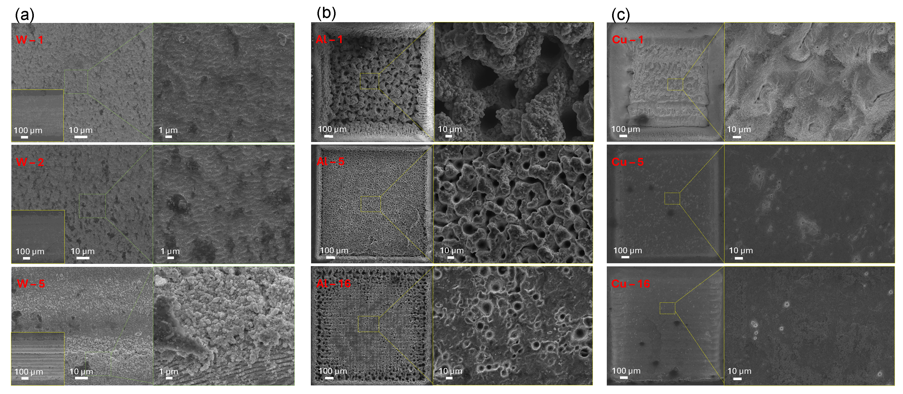
3.1. Ablation with High-Intensity fs-Laser Pulses

Ablation experiments for W, Al, and Cu metals with the electron work functions: w e = 4.55 eV (polycrystalline W), 4.06–4.2 eV (Al), 4.48–5.1 eV (different planes of Cu) were performed at the fundamental laser radiation wavelength of 1030 nm with a beam diameter on the surface of 2 r = 60 μ m. Hatching between adjacent lines was fixed at Δ y = 50 μ m, which is slightly smaller than the focal diameter. For the tungsten sample (Figure 1a), the linear beam travel speed was set as v s c = 1000 25 mm/s along the x-direction at a repetition rate of 100 kHz, producing pulse-to-pulse spacing of 10–0.2 μ m. The fluence per pulse was fixed at F p = 24.76 J/cm2 corresponding to the pulse energy of E p = 0.7 mJ and the pulse duration of t p = 200 fs; the average intensity per pulse is I p = F p / t p = 123.8 TW/cm2. A combination of the different pulse spacings with a single pass or five passes was performed.
For aluminum and copper (Figure 1b,c), a total of 16 ablation areas were fabricated on each metal coupon’s surface, defining the ablation matrix of the various pulse spacings 42–7 μ m with different fluence per pulse 28.3–5.7 J/cm2. Each ablated area, created under specific ablation conditions, was labeled with numbers (W: 1–6, Al: 1–16, Cu: 1–16) to align with the subsequent characterization results (Figure 1).
The tested metals are very different in their physico-chemical properties. The molar enthalpy of vaporization (atomization) of Cu is 300 kJ/mol (338 kJ/mol), for Al 293 kJ/mol (326 kJ/mol), and for W 807 kJ/mol (849 kJ/mol, the highest among chemical elements). The enthalpy of vaporization recalculated per atom is 3.11 eV/atom (Cu), 3.04 eV/atom (Al), and 8.36 eV/atom (W). Solid densities for Cu of ρ C u = 8920 kg·m−3 (molar volume V m ( C u ) = 7.11 cm3 and molar mass M C u = 63.546 g/mol), Al of ρ A l = 2700 kg·m−3 ( V m ( A l ) = M A l ρ A l = 10 cm3 where molar mass M A l = 26.98154 g/mol), and W of ρ W = 19280 kg·m−3 ( V m ( W ) = 9.54 cm3 and molar mass M W = 183.84 g/mol) were found.
The ablation threshold for metals can be estimated by Gamaly’s model for the pulse fluence [37]. According to it, the ablation is initiated by depositing energy to electrons equal to the material’s binding energy and the electron work function [37]:
F t h ( m ) = 3 8 ( ϵ b + w e ) λ n e 2 π ,
where ϵ b is the binding energy or enthalpy of vaporization, w e is the electron work function (escape energy from a metal), l s = c / ( ω κ ) λ / ( 2 π κ ) is the absorption depth (the skin depth) in the plasma with electron density n e and refractive index n = n + i κ with c and ω being the speed and cyclic frequency of light, respectively, and A is the absorption coefficient (for good metals A 2 ω l s c ). To estimate the ablation thresholds, the smallest of the listed w e [eV] and binding energy per atom ϵ b [eV] values were used. The electron density is estimated considering one electron per atom donated to metallic bonding n e ( m ) = N A / V m ( m ) , where N A [mol−1] is the Avogadro number and V m ( m ) [cm3] is the molar volume calculated above. With all parameters defined and λ = 1030 nm, the following ablation thresholds are obtained from Equation (1): 0.40 J/cm2 (Cu), 0.26 J/cm2 (Al), 0.34 J/cm2 (W). These are single-pulse ablation thresholds. As the surface is ablated and reflectivity is gradually reduced with subsequent pulses, the accumulation dose or F p times the number of pulses N per spot of diameter D: N = D / v s / f at scanning speed v s and laser repetition rate f can reach the ablation threshold even at slightly lower pulse energies.
The experiments in this study were carried out at an irradiance up to 30–100 times above the threshold; moreover, with up to N = 10 pulses per focal spot. Hard X-rays generated at such conditions [38] require the screening enclosure of the sample chamber, especially when multi-pulse or burst modes of exposure are used [39].

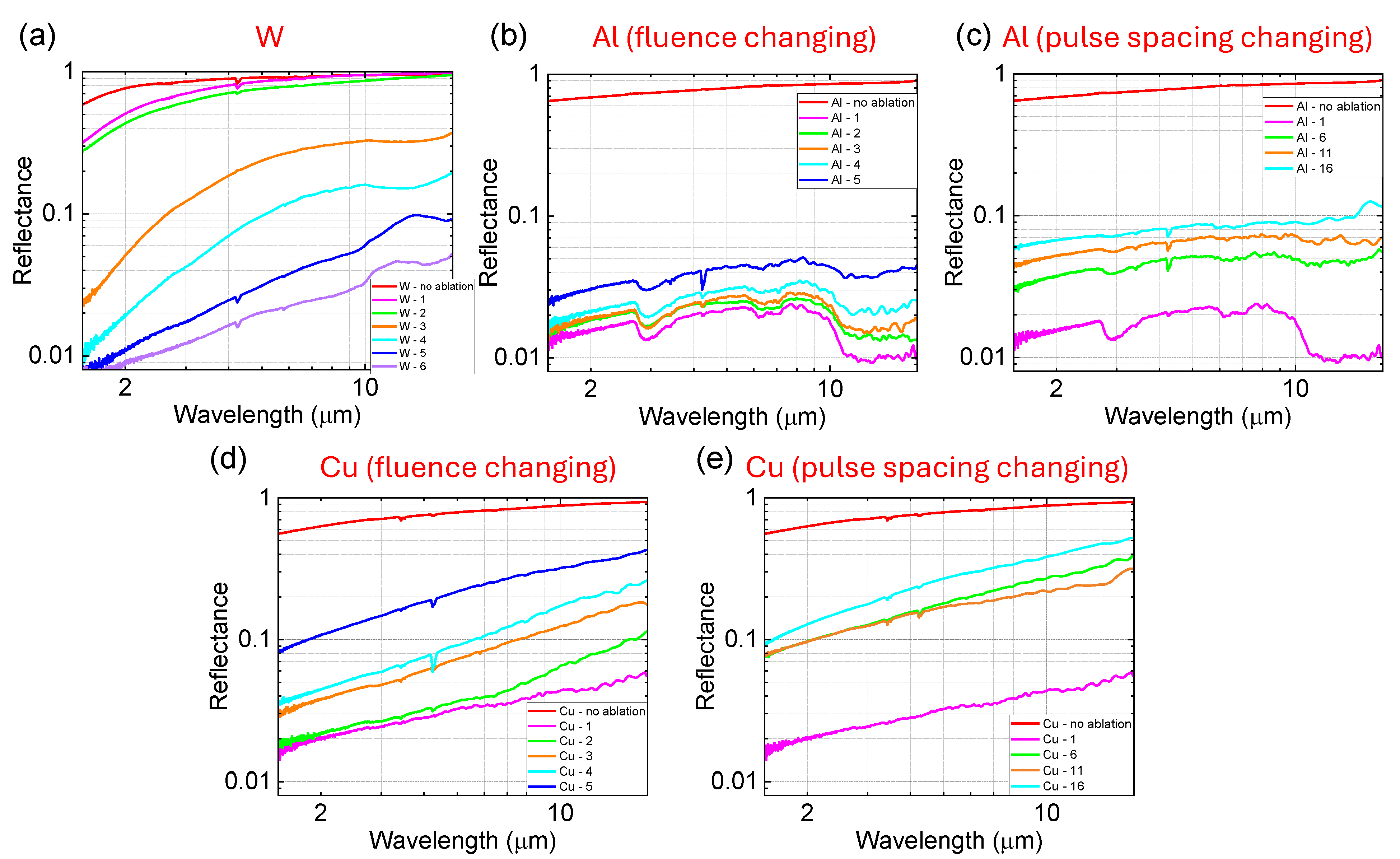
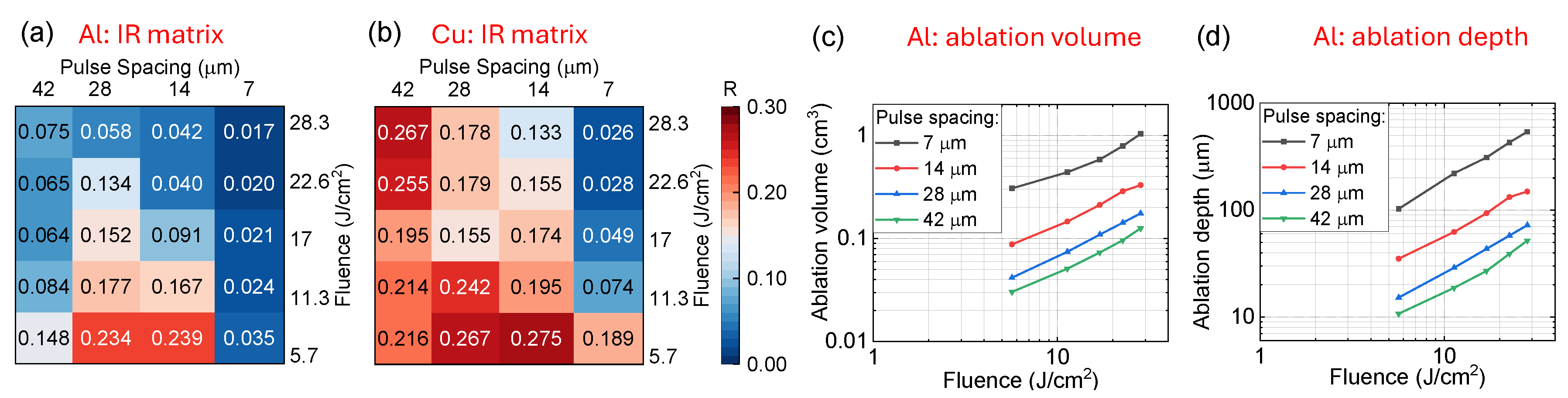
3.2. Reflectivity of Laser Ablated Surfaces at IR Spectral Range

The ablated area on W, Al, and Cu samples shows a black appearance in the visible spectral range. The reflectance of these black surfaces was tested at near-to-mid IR range 1.5–18 μ m shown in Figure 3 corresponding to the labeled areas on the samples (Figure 1). The IR reflectance shows a clear reduction in reflectance for all ablated metals: R < 40 % (W), R < 15 % (Al), R < 55 % (Cu), compared with the non-ablated surfaces R 98 % (W), R 90 % (Al), and R 95 % (Cu). The anti-reflectance effect is positively related to the energy deposited on metal surfaces, i.e., the higher energy deposition (higher fluence and smaller pulse spacing) produces surfaces with a smaller R at the IR window. The lowest reflectance for each sample was R < 5 % (W–6), R < 3 % (Al–1) and R < 6 % (Cu–1) corresponding to a formidable reflectance decrease of around 90%. The formation of Al2O3 is recognizable by its absorbance around ∼6 μ m in the reflectivity spectra. The so-called water absorption band associated with a 3–3.5 μ m window is due to Al–OH (a decrease in reflectivity due to absorption).
Figure 4a,b summarizes the reflectance R over the measured λ = 1.5–18 μ m window for the 4 × 5 matrix of S p a c i n g × F l u e n c e for Al and Cu. Apparently, the highest fluence at the strongest pulse-to-pulse overlap produced the lowest reflective surfaces for Al and Cu. This corresponded to the largest ablated volume as shown in Figure 4c. For the different Δ x , y pulse overlaps, a linear scaling of ablated volume V a l F p as well as the depth H a b F p was observed.
The surface morphology at different magnifications was inspected with SEM and shown in Figure 5 for specific fluence and pulse overlap conditions. Very different surface nano-micro topographies are observed from ripples with a period close to the laser wavelength ∼1 μ m to the structures with dimensions close to the focal spot size of ∼40 μ m. The most anti-reflective pattern on Al (in (b)) had the richest 3D topography. The conical inverted pyramidal structures are apparent as holes on the surface were clearly observed on Al, which has the lowest melting temperature of 660 °C compared with Cu (1084 °C) and W (3422 °C).
The most complex 3D textures were observed on Al, which has the lowest melting temperature among tested metals. The feature size of conical holes in Al is close to the full width at half-maximum (FWHM) measure of the focal spot size. The photon pressure exerted by a pulse of irradiance I p = 100 TW/cm2 or 10 18 W/m2 is P p h = I p / c 1 3 × 10 10 Pa = 3.3 GPa, where c 3 × 10 8 m/s is the speed of light. This pressure is applied when the fs-laser pulse energy is deposited (absorbed), while the reflection doubles it via the momentum transfer due to the reversal of the photon direction. Hence, the laser peening is present. The imparted pressure is a contributing factor to the formation of surface textures guided by an interplay of Al softening/melting together with fast thermal quenching due to high thermal conductivity.
The structural color effect due to the surface morphology is an obvious contributor to the anti-reflective (color-black) appearance at vis-IR spectral ranges. However, the chemical modification of metal surfaces processed in air under ambient conditions has to be assessed as well, especially when it is relevant to very different perspectives of applications. For Al and Cu, which are both very chemically active and were processed at an energy condition exceeding their ablation threshold by more than 30 times, chemical modifications were scrutinized using XPS and EDS as discussed next.

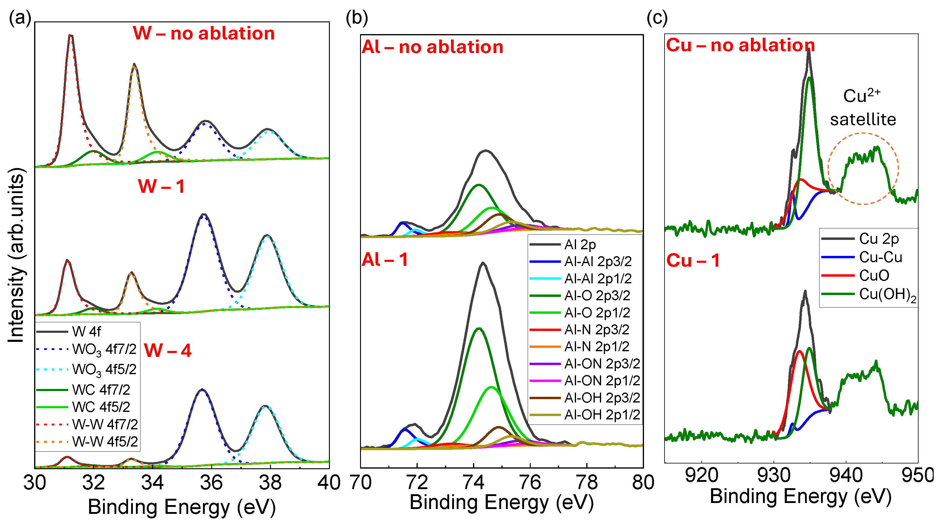
3.3. Surface Chemistry on Surfaces Ablated at Tens-of-TW/cm2 Fluence

Figure 6 shows XPS spectra at the metal-specific binding energy window, which was analyzed by peak fitting and area comparison for quantitative analysis. Table 1, Table 2 and Table 3 summarize the quantitative XPS results and reveal intricate changes in chemical bonding on the surface of tungsten, aluminum, and copper, respectively, before and after laser ablation.
The tungsten sample showed a notable increase in metal oxidation with WO3 bonding increasing from 30.22% (W – no ablation) to 91.22% (W – 4); the oxidation is proportional to the amount of energy deposited on the surface (Table 1). This indicates that oxidation was taking place at high-temperature conditions, which is required for the inert metal W. Fs-laser pulses engraved nanostructures, such as protrusions and ripples on W–metal surfaces, which can be oxidized at elevated temperatures in air [40]. The equation-of-state (EoS) of W from cryogenic to melting temperatures has been recently proposed [41] and can predict the high-temperature and high-pressure response of W.
The ablated aluminum surface showed an increased percentage of Al–O bonding, which is consistent with previous findings [30,42]. The Al–O bonding increased from 61.46% to 76.80% while the Al–OH bonding dropped from 18.01% on the pristine Al surface to 8.84% on the ablated surface (Table 2). Apparently, the top layer of hydroxide was removed by ablation, and oxidation was prevalent on a nano-micro rough surface with an Al 2 O 3 layer well in line with the earlier study [30]. The oxidation might be influenced by two possible mechanisms. One is the oxidation of aluminum due to the sample’s exposure to air after laser ablation. The other is the interaction between aluminum ions in plasma and oxygen with re-deposition onto the sample surface. A very fast oxidation/passivation process of Al takes place at the ∼1050–1150 °C window, but a distinct incubation time was required for oxidation above ∼850 °C as found in a recent study by differential scanning calorimetry [43]. When Al was preheated to high temperatures with oxygen, the oxidation progressed with the expansion and growth of the material, thus different granular structures were formed with thicknesses up to micrometers [43]. The evaporation of Al and initial mass loss in Ar at high temperatures was proportional to the Al vapor pressure.
The copper sample shows a strong Cu 2 + satellite peak around 943 eV, indicating that the oxidation form is the cuprix Cu(II) oxide CuO. The oxidation state of copper was found to be dependent on the ablation conditions, e.g., CuO is formed at a lower beam velocity of 20 mm/s, while Cu 2 O tends to form at a higher velocity of 100 mm/s [36]. Similar to the Al surface, laser ablation changed the surface composition of the copper compound, with CuO increasing from 27.57% to 58.80% and Cu ( OH ) 2 decreasing from 66.50% to 39.10% (Table 3). The oxidation of Cu under fs-laser ablation can explain the color (in visible light) appearance of surfaces due to the thin oxide layer [27]. Understanding the laser processing parameters that can control Cu oxide formation on laser-ablated ripples is important for photo-cathode applications [44].
High-intensity laser pulses trigger strong thermal gradients, enhancing the oxidation process [45] and metal compounds are shifted towards metal oxides. Oxides are thermodynamically stable and dominate over the formation of hydroxides, carbides, nitrides, and oxynitrides consistent with findings in this study (Table 1, Table 2 and Table 3). Metal oxides, such as Al 2 O 3 , WO 3 , and CuO have a lower refractive index and contribute, in part, to the reduction in reflectance. This observation aligns with broadband simulation results, which demonstrate that the thickness of metal oxide layers improves surface emissivity [46]. The 3D textured structure on the ablated metal surfaces also traps light and contributes to the reduction in reflectance, and the depth/height of microstructure contributes to emissivity enhancement due to lower reflectance [46].
Elemental analysis was also carried out using EDS. The results are summarized in Table 4. Since EDS determines the elemental composition and is not sensitive to the chemical bonding, as well as probing the larger micrometer-scale depth from which X-rays can escape, the results are different from XPS and have a qualitative character. A surprising observation was the unusual carbon content in as-received Cu coupons, which were cut by a standard mechanical saw tool with oil used as a cooling agent. All samples were IPA washed before experiments; however, only Cu showed C contamination in the EDS measurements. After ablation, only oxygen was detected in addition to Cu. In all W, Al, and Cu samples, the metal content exceeded that of the known oxides and O-containing surface compounds. This is expected due to the large micron depth of EDS probing since oxides are on the surface at the nanoscale.

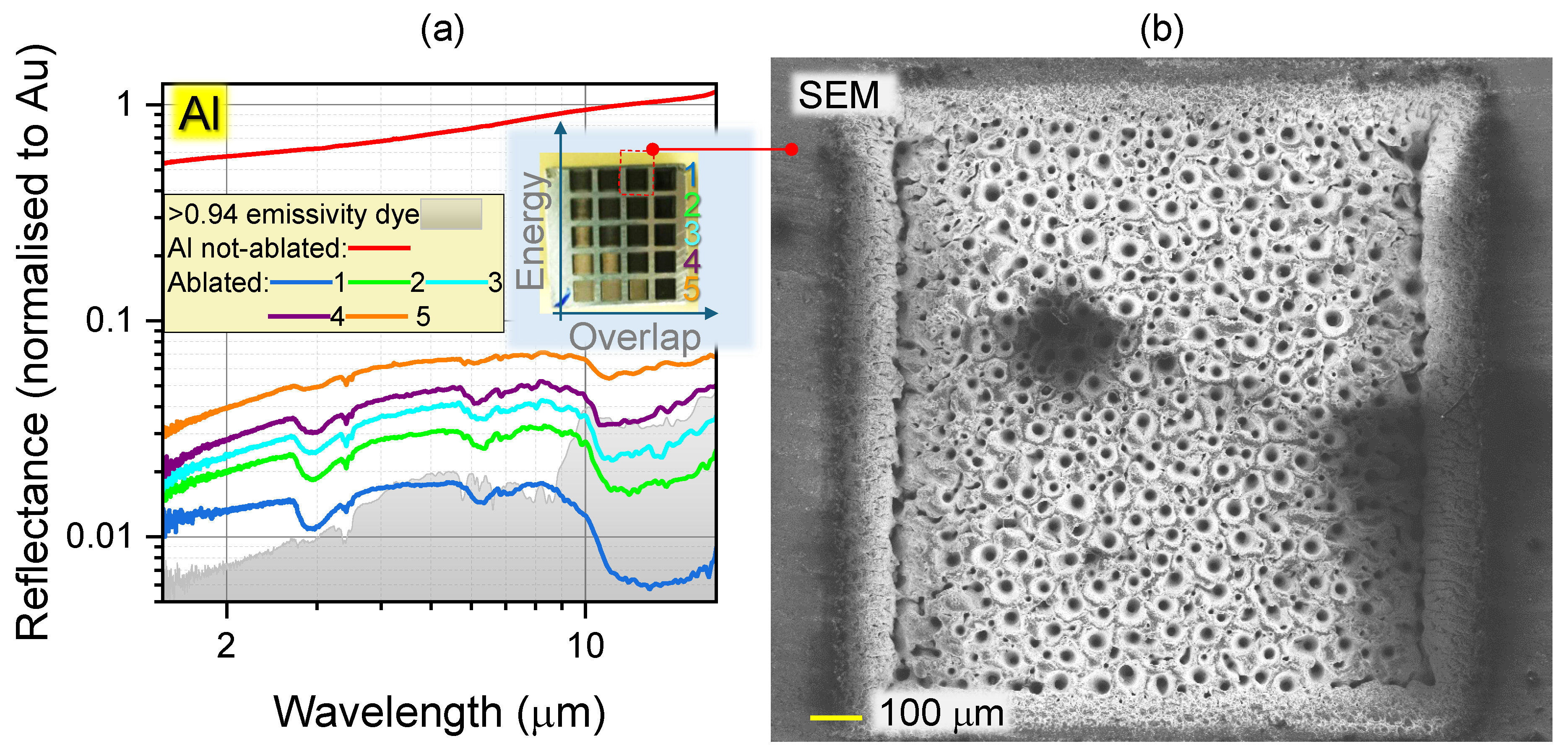
3.4. Radiative Cooling Effect of Black Metals

Black (anti-reflective) metal surfaces have great potential for applications in radiative cooling when the low reflectance is in the mid-IR 1.5–18 μ m spectral range [47,48,49]. Physical effects, such as surface roughness are known to alter emissivity, which is also affected by the surface composition/chemistry [50,51,52]. Fs-laser texturing is a simple and increasingly practical method to create nano-micro rough textures over large surface areas [27,53]. Such fs-laser-textured surfaces are of interest for catalytic applications [30] not only due to the larger surface area but also due to reduced reflectivity in photo-catalytic applications [54]. The spectrally broad reduction in IR reflectivity demonstrated here can expand the application potential of narrow IR band emitters based on perfect absorbers [4], which can also be made out of high entropy alloys (HEA) [55,56] which is promising for industrial applications including at high temperatures.
Tungsten is a unique material due to its highest melting temperature, very large mass density, chemical inertness, and comparatively low thermal expansion. Its applications can be found from ink spreading ball in a ball pen, served/serves as a lightning filament in incandescent lamps to industry/defense/space industries where surfaces are subjected to extreme temperatures in plane/rocket engines or power plants. The W and WC surfaces with anti-reflective features made by fs-laser texturing can be efficient emitters based on Kirchhoff’s law when heated at very high temperatures ∼3000 °C to cool down surfaces. Moreover, thermal energy harvesting can be more efficient as predicted by Carnot’s limit of efficiency η C = 1 T c o l d / T h o t ; T c o l d = 3 K at outer space [47]. Thermal radiation harvesting is promising due to its high efficiency [57].

4. Conclusions and Outlook

Laser ablation of the metals W, Al, and Cu by ultra-short 200 fs laser pulses at high 20–120 TW/cm2 average intensity/irradiance with a large focal area (∼60 μ m diameter) produced complex hierarchical 3D surface textures with features ranging from ripples of wavelength ∼1 μ m to inverted pyramidal cones (most typical on Al) with openings of tens-of-micrometers. The most complex 3D textures with the largest depth changing were on Al, which has the lowest melting temperature among the metals investigated here. The primary chemical change observed in the outer surface layers through XPS was the formation of oxides, which correlates with the reflectance reduction due to the lower refractive index of metal oxides. Interestingly, the ablation, which starts as an electron removal from the surface after energy deposition, is synonymous with oxidation, which is the loss of electrons by definition. Ablation at an energy deposition up to 100 × times larger than the threshold fluence/intensity facilitates a high local temperature, material flow driven by strong thermal gradients, oxidation, and subsequent thermal quenching. This process results in an ablation depth of 10 1 10 3   μ m, producing complex 3D inverted pyramidal-shaped oxides that contribute to approximately a 55–95% reduction in reflectance compared to the original metal surfaces.
In the context of radiative cooling, the oxidation and passivation of metal surfaces are expected to enhance thermal emissivity, which is structure and morphology-dependent. Metals are naturally reflective with low emissivity, but the formation of oxide layers and increased surface roughness, which render them anti-reflective, are favorable for radiative cooling, especially at elevated temperatures relevant to industrial and space applications. This work has demonstrated that laser ablation with an industrial fs-laser of 80 W power at a fast scan rate can be used to create low-reflectivity surfaces across the 2–20 μ m near- to mid-IR spectral window.

Author Contributions

Conceptualization, R.B., H.-H.H. and S.J.; methodology, N.Z., R.B., H.-H.H. and T.K.; software, R.B., M.K. and T.K.; validation, N.Z., D.S., S.P., D.M.Z., L.G. and P.R.S.; formal analysis, N.Z. and R.B.; investigation, N.Z.; resources, P.R.S.; data curation, R.B., N.Z. and Y.N.; writing—original draft preparation, S.J., N.Z. and H.-H.H.; writing—review and editing, all the authors; visualization, N.Z. and S.J.; supervision, R.B.; project administration, R.B.; funding acquisition, R.B. and P.R.S. All authors have read and agreed to the published version of the manuscript.

Funding

This research was partly funded by the Australian Research Council Linkage LP220100153 and Discovery DP240103231 grants.

Data Availability Statement

All the data are presented within this manuscript.

Acknowledgments

We acknowledge support by Swinburne University of Technology for lab allocation to test 80 W fs-laser machining system. We are grateful to Jeremy Brown for radiation safety discussions.

Conflicts of Interest

Author Ričardas Buividas was employed by the company Quoba Systems Pty. Ltd. All authors declare that the research was conducted without any commercial or financial relationships that could be construed as a potential conflict of interest.

References

  1. Lundgaard, S.; Ng, S.H.; Nishijima, Y.; Mazilu, M.; Juodkazis, S. Black Metals: Optical Absorbers. Micromachines 2020, 11, 256. [Google Scholar] [CrossRef] [PubMed]
  2. Ivanova, E.P.; Hasan, J.; Webb, H.K.; Gervinskas, G.; Juodkazis, S.; Truong, V.K.; Wu, A.H.F.; Lamb, R.N.; Baulin, V.A.; Watson, G.S.; et al. Bactericidal activity of black silicon. Nat. Commun. 2013, 4, 2838. [Google Scholar] [CrossRef] [PubMed]
  3. Cunha, N.F.; AL-Rjoub, A.; Rebouta, L.; Vieira, L.G.; Lanceros-Mendez, S. Multilayer passive radiative selective cooling coating based on Al/SiO2/SiNx/SiO2/TiO2/SiO2 prepared by dc magnetron sputtering. Thin Solid Film. 2020, 694, 137736. [Google Scholar] [CrossRef]
  4. To, N.; Juodkazis, S.; Nishijima, Y. Detailed Experiment-Theory Comparison of Mid-Infrared Metasurface Perfect Absorbers. Micromachines 2020, 11, 409. [Google Scholar] [CrossRef] [PubMed]
  5. Liao, J.; Zhang, D.; Li, Z. Conceptional Pure-Tungsten Metasurfaces Based on Femtosecond Laser Nanomanufacturing. Engineering 2024, in press. [Google Scholar] [CrossRef]
  6. Xiao, W.; Dai, P.; Singh, H.J.; Ajia, I.A.; Yan, X.; Wiecha, P.R.; Huang, R.; de Groot, C.H.K.; Muskens, O.L.; Sun, K. Flexible thin film optical solar reflectors with Ta2O5-based multimaterial coatings for space radiative cooling. APL Photonics 2023, 8, 090802. [Google Scholar] [CrossRef]
  7. Tu, H.; Pan, L.; Qi, H.; Zhang, S.; Li, F.; Sun, C.; Wang, X.; Cui, T. Ultrafast dynamics under high-pressure. J. Phys. Condens. Matter 2023, 35, 253002. [Google Scholar] [CrossRef]
  8. Xu, L.; Tao, J.; Li, Z.; He, G.; Zhang, D. Femtosecond laser ultrafast photothermal exsolution. Int. J. Extrem. Manuf. 2024, 6, 055002. [Google Scholar] [CrossRef]
  9. Jiang, R.; Da, Y.; Han, X.; Chen, Y.; Deng, Y.; Hu, W. Ultrafast Synthesis for Functional Nanomaterials. Cell Rep. Phys. Sci. 2021, 2, 100302. [Google Scholar] [CrossRef]
  10. Rezayat, M.; Roa, J.J.; Mateo, A. Effect of Laser Surface Texturing on Schmid Factor and Plastic Deformation Mechanisms on AISI 301LN Steel. Metals 2023, 13, 1789. [Google Scholar] [CrossRef]
  11. Morales, M.; Rezayat, M.; Mateo, A. Enhancing the corrosion resistance of 2205 duplex stainless steel in molten carbonate salts by laser-surface texturing. J. Energy Storage 2024, 78, 110053. [Google Scholar] [CrossRef]
  12. Rezayat, M.; Rovira, J.J.R.; García, A.M. Phase transformation and residual stresses after laser surface modification of metastable austenitic stainless steel. AIP Conf. Proc. 2023, 2848, 020005. [Google Scholar] [CrossRef]
  13. Juodkazis, S.; Nishimura, K.; Tanaka, S.; Misawa, H.; Gamaly, E.G.; Luther-Davies, B.; Hallo, L.; Nicolai, P.; Tikhonchuk, V.T. Laser-Induced Microexplosion Confined in the Bulk of a Sapphire Crystal: Evidence of Multimegabar Pressures. Phys. Rev. Lett. 2006, 96, 166101. [Google Scholar] [CrossRef] [PubMed]
  14. Rapp, L.; Haberl, B.; Pickard, C.; Bradby, J.; Gamaly, E.; Williams, J.; Rode, A. Experimental evidence of new tetragonal polymorphs of silicon formed through ultrafast laser-induced confined microexplosion. Nat Commun 2015, 6, 7555. [Google Scholar] [CrossRef] [PubMed]
  15. Rapp, L.; Matsuoka, T.; Firestein, K.L.; Sagae, D.; Habara, H.; Mukai, K.; Tanaka, K.A.; Gamaly, E.G.; Kodama, R.; Seto, Y.; et al. Observation of high-pressure polymorphs in bulk silicon formed at relativistic laser intensities. Phys. Rev. Res. 2024, 6, 023101. [Google Scholar] [CrossRef]
  16. Xu, K.M.; L, C.; Wang, L.; Pang, F.C.; Zhao, X.J.; Li, X.B.; Chen, Q.D.; Zhao, W.Q. Ultrafast laser-induced decomposition for selective activation of GaAs. Light. Adv. Manuf. 2024, 5, 241. [Google Scholar] [CrossRef]
  17. Maksimovic, J.; Mu, H.; Han, M.; Smith, D.; Katkus, T.; Anand, V.; Nishijima, Y.; Ng, S.H.; Juodkazis, S. Si-Cr Nano-Alloys Fabricated by Direct Femtosecond Laser Writing. Materials 2023, 16, 1917. [Google Scholar] [CrossRef]
  18. Maksimovic, J.; Hu, J.; Ng, S.; Katkus, T.; Seniutinas, G.; Pinedo Rivera, T.; Stuiber, M.; Nishijima, Y.; John, S.; Juodkazis, S. Beyond Lambertian light trapping for large-area silicon solar cells: Fabrication methods. Opto-Electron Adv 2022, 5, 210086. [Google Scholar] [CrossRef]
  19. Zograf, G.; Koshelev, K.; Zalogina, A.; Korolev, V.; Hollinger, R.; Choi, D.Y.; Zuerch, M.; Spielmann, C.; Luther-Davies, B.; Kartashov, D.; et al. High-Harmonic Generation from Resonant Dielectric Metasurfaces Empowered by Bound States in the Continuum. ACS Photonics 2022, 9, 567–574. [Google Scholar] [CrossRef]
  20. Ueno, K.; Juodkazis, S.; Shibuya, T.; Mizeikis, V.; Yokota, Y.; Misawa, H. Nanoparticle-Enhanced Photopolymerization. J. Phys. Chem. C 2009, 113, 11720–11724. [Google Scholar] [CrossRef]
  21. Samsonas, D.; Skliutas, E.; Čiburys, A.; Kontenis, L.; Gailevičius, D.; Berzinš, J.; Narbutis, D.; Jukna, V.; Vengris, M.; Juodkazis, S.; et al. 3D nanopolymerization and damage threshold dependence on laser wavelength and pulse duration. Nanophotonics 2023, 12, 1537–1548. [Google Scholar] [CrossRef] [PubMed]
  22. Katkus, T.; Ng, S.H.; Mu, H.; Le, N.H.A.; Stonytė, D.; Khajehsaeidimahabadi, Z.; Seniutinas, G.; Baltrukonis, J.; Ulčinas, O.; Mikutis, M.; et al. Bessel-Beam Direct Write of the Etch Mask in a Nano-Film of Alumina for High-Efficiency Si Solar Cells. Adv. Eng. Mater. 2024, 26, 2400711. [Google Scholar] [CrossRef]
  23. Zhu, Z.; Wu, P.; Juodkazis, S.; Wang, J.; Yao, S.; Yao, J.; Zhang, W. Superhydrophobic and Anti-Icing Surface by Femtosecond Laser Direct Writing. Adv. Eng. Mater. 2023, 25, 2300575. [Google Scholar] [CrossRef]
  24. Myronyuk, O.; Baklan, D.; Rodin, A.M.; Vanagas, E.; Yong, Z. Owens–Wendt Characterization of Femtosecond-Laser-Textured Hydrophobic Aluminum Surfaces. Coatings 2023, 13, 1104. [Google Scholar] [CrossRef]
  25. Myronyuk, O.; Vanagas, E.; Rodin, A.M.; Wesolowski, M. Estimation of the Structure of Hydrophobic Surfaces Using the Cassie–Baxter Equation. Materials 2024, 17, 4322. [Google Scholar] [CrossRef]
  26. Kadys, A.; Mickevičius, J.; Badokas, K.; Strumskis, S.; Vanagas, E.; Podlipskas, v.; Ignatjev, I.; Malinauskas, T. Epitaxial Lateral Overgrowth of GaN on a Laser-Patterned Graphene Mask. Nanomaterials 2023, 13, 784. [Google Scholar] [CrossRef]
  27. Zheng, N.; Buividas, R.; Huang, H.H.; Stonytė, D.; Palanisamy, S.; Katkus, T.; Kretkowski, M.; Stoddart, P.R.; Juodkazis, S. Laser Machining at High ∼PW/cm2 Intensity and High Throughput. Photonics 2024, 11, 598. [Google Scholar] [CrossRef]
  28. Gorham, J. NIST X-Ray Photoelectron Spectroscopy Database—SRD 20; U. S. Department of Commerce: Washington, DC, USA, 2012. [CrossRef]
  29. Dallaev, R.; Sobola, D.; Tofel, P.; Škvarenina, L.; Sedlák, P. Aluminum Nitride Nanofilms by Atomic Layer Deposition Using Alternative Precursors Hydrazinium Chloride and Triisobutylaluminum. Coatings 2020, 10, 954. [Google Scholar] [CrossRef]
  30. Balchev, I.; Minkovski, N.; Marinova, T.; Shipochka, M.; Sabotinov, N. Composition and structure characterization of aluminum after laser ablation. Mater. Sci. Eng. B 2006, 135, 108–112. [Google Scholar] [CrossRef]
  31. Xu, R.; Xie, Y.; Li, R.; Zhang, J.; Zhou, T. Direct Bonding of Polymer and Metal with an Ultrahigh Strength: Laser Treatment and Mechanical Interlocking. Adv. Eng. Mater. 2021, 23, 2001288. [Google Scholar] [CrossRef]
  32. Ardelean, H.; Petit, S.; Laurens, P.; Marcus, P.; Arefi-Khonsari, F. Effects of different laser and plasma treatments on the interface and adherence between evaporated aluminium and polyethylene terephthalate films: X-ray photoemission, and adhesion studies. Appl. Surf. Sci. 2005, 243, 304–318. [Google Scholar] [CrossRef]
  33. Lizarbe, A.J.; Major, G.H.; Fernandez, V.; Fairley, N.; Linford, M.R. Insight note: X-ray photoelectron spectroscopy (XPS) peak fitting of the Al 2p peak from electrically isolated aluminum foil with an oxide layer. Surf. Interface Anal. 2023, 55, 651–657. [Google Scholar] [CrossRef]
  34. Biesinger, M.C. Advanced analysis of copper X-ray photoelectron spectra. Surf. Interface Anal. 2017, 49, 1325–1334. [Google Scholar] [CrossRef]
  35. Biesinger, M.C.; Lau, L.W.M.; Gerson, A.R.; Smart, R.S.C. Resolving surface chemical states in XPS analysis of first row transition metals, oxides and hydroxides: Sc, Ti, V, Cu and Zn. Appl. Surf. Sci. 2010, 257, 887–898. [Google Scholar] [CrossRef]
  36. Stefanov, P.; Minkovski, N.; Balchev, I.; Avramova, I.; Sabotinov, N.; Marinova, T. XPS studies of short pulse laser interaction with copper. Appl. Surf. Sci. 2006, 253, 1046–1050. [Google Scholar] [CrossRef]
  37. Gamaly, E.G.; Rode, A.V.; Luther-Davies, B. Ablation of solids by femtosecond lasers: Ablation mechanism and ablation thresholds for metals and dielectrics. Phys. Plasmas 2002, 18, 949–957. [Google Scholar] [CrossRef]
  38. Rimkus, L.; Stasevičius, I.; Barkauskas, M.; Giniūnas, L.; Barkauskas, V.; Butkus, S.; Vengris, M. Compact high-flux X-ray source based on irradiation of solid targets by gigahertz and megahertz bursts of femtosecond laser pulses. Opt. Contin. 2022, 1, 1819–1836. [Google Scholar] [CrossRef]
  39. Schille, J.; Kraft, S.; Pflug, T.; Scholz, C.; Clair, M.; Horn, A.; Loeschner, U. Study on X-ray Emission Using Ultrashort Pulsed Lasers in Materials Processing. Materials 2021, 14, 4537. [Google Scholar] [CrossRef]
  40. Jalil, S.A.; Lai, B.; ElKabbash, M.; Zhang, J.; Garcell, E.M.; Singh, S.; Guo, C. Spectral absorption control of femtosecond laser-treated metals and application in solar-thermal devices. Light. Sci. Appl. 2020, 9, 14. [Google Scholar] [CrossRef]
  41. Kozyrev, N.V.; Gordeev, V.V. Thermodynamic Properties and Equation of State for Tungsten. Crystals 2023, 13, 1470. [Google Scholar] [CrossRef]
  42. Atanasov, P.; Dikovska, A.; Nikov, R.; Atanasova, G.; Grochowska, K.; Karczewski, J.; Fukata, N.; Jevasuwan, W.; Nedyalkov, N. Surface-Enhanced Raman Spectroscopy of Ammonium Nitrate Using Al Structures, Fabricated by Laser Processing of AlN Ceramic. Materials 2024, 17, 2254. [Google Scholar] [CrossRef] [PubMed]
  43. Coker, E.N.; Donaldson, B.; Gill, W.; Yilmaz, N.; Vigil, F.M. The Isothermal Oxidation of High-Purity Aluminum at High Temperature. Appl. Sci. 2023, 13, 229. [Google Scholar] [CrossRef]
  44. Martinez-Calderon, M.; Groussin, B.; Bjelland, V.; Chevallay, E.; Fedosseev, V.N.; Himmerlich, M.; Lorenz, P.; Manjavacas, A.; Marsh, B.A.; Neupert, H.; et al. Hot electron enhanced photoemission from laser fabricated plasmonic photocathodes. Nanophotonics 2024, 13, 1975–1983. [Google Scholar] [CrossRef] [PubMed]
  45. Parris, G.; Goel, S.; Nguyen, D.T.; Buckeridge, J.; Zhou, X. A critical review of the developments in molecular dynamics simulations to study femtosecond laser ablation. Mater. Today Proc. 2022, 64, 1339–1348. [Google Scholar] [CrossRef]
  46. Qi, J.Y.; Liu, X.Q.; Liu, Z.J.; Zhang, X.; Li, C.; Chen, Q.D.; Wang, L.; Sun, H.B. Ultrawide Spectrum Metallic Plane Blackbody with Extremely High Absorption from 0.2 to 25 μm. Adv. Sci. 2025, 12, 2411448. [Google Scholar] [CrossRef]
  47. Chen, Z.; Zhu, L.; Raman, A.; Fan, S. Radiative cooling to deep sub-freezing temperatures through a 24-h day–night cycle. Nat. Commun. 2016, 7, 13729. [Google Scholar] [CrossRef] [PubMed]
  48. Aili, A.; Jiang, T.; Chen, J.; Wen, Y.; Yang, R.; Yin, X.; Tan, G. Passive daytime radiative cooling: Moving beyond materials towards real-world applications. Next Energy 2024, 3, 100121. [Google Scholar] [CrossRef]
  49. Zhou, L.; Rada, J.; Tian, Y.; Han, Y.; Lai, Z.; McCabe, M.F.; Gan, Q. Radiative cooling for energy sustainability: Materials, systems, and applications. Phys. Rev. Mater. 2022, 6, 090201. [Google Scholar] [CrossRef]
  50. Ventola, L.; Robotti, F.; Dialameh, M.; Calignano, F.; Manfredi, D.; Chiavazzo, E.; Asinari, P. Rough surfaces with enhanced heat transfer for electronics cooling by direct metal laser sintering. Int. J. Heat Mass Transf. 2014, 75, 58–74. [Google Scholar] [CrossRef]
  51. Zhou, F.; DeMoulin, G.W.; Geb, D.J.; Catton, I. Closure for a plane fin heat sink with scale-roughened surfaces for volume averaging theory (VAT) based modeling. Int. J. Heat Mass Transf. 2012, 55, 7677–7685. [Google Scholar] [CrossRef]
  52. Suryawanshi, C.N.; Lin, C.T. Radiative Cooling: Lattice Quantization and Surface Emissivity in Thin Coatings. ACS Appl. Mater. Interfaces 2009, 1, 1334–1338. [Google Scholar] [CrossRef] [PubMed]
  53. Sciti, D.; Trucchi, D.M.; Bellucci, A.; Orlando, S.; Zoli, L.; Sani, E. Effect of surface texturing by femtosecond laser on tantalum carbide ceramics for solar receiver applications. Sol. Energy Mater. Sol. Cells 2017, 161, 1–6. [Google Scholar] [CrossRef]
  54. Linklater, D.P.; Haydous, F.; Xi, C.; Pergolesi, D.; Hu, J.; Ivanova, E.P.; Juodkazis, S.; Lippert, T.; Juodkazytė, J. Black-Si as a Photoelectrode. Nanomaterials 2020, 10, 873. [Google Scholar] [CrossRef] [PubMed]
  55. Nishijima, Y.; Sudo, T.; Matsuo, Y.; Juodkazis, S. Noble metal high entropy alloy for mid infrared metasurfaces. ChemRxiv 2023, preprint. [Google Scholar] [CrossRef]
  56. Han, M.; Meghwal, A.; Ng, S.H.; Smith, D.; Mu, H.; Katkus, T.; Zhu, D.M.; Mukhlis, R.; Vongsvivut, J.; Berndt, C.C.; et al. Microparticles of High Entropy Alloys Made by Laser-Induced Forward Transfer. Materials 2022, 15, 8063. [Google Scholar] [CrossRef]
  57. Buddhiraju, S.; Santhanam, P.; Fan, S. Thermodynamic limits of energy harvesting from outgoing thermal radiation. Proc. Natl. Acad. Sci. USA 2018, 115, E3609–E3615. [Google Scholar] [CrossRef]
Figure 1. Fs-laser ablation of (a) tungsten with various pulse spacing (10–0.25 μ m) and number of passes (1, 5), (b) aluminum with various pulse spacing (42–7 μ m) and fluence per pulse (28.3–5.7 J/cm2), (c) copper (the same ablation condition as aluminum).
Applsci 15 02076 g001
Figure 2. (a) Reflectance of Al after ablation by 1030 nm/200 fs/0.1 MHz irradiation at different scanning speeds corresponding to different in-line separation between pulses Δ x = (7–42) μ m (1-to-5) and different pulse energies E p = 0.8 mJ (1) to 0.16 mJ (5). The focal spot size is 60 μ m; the inset photo shows a test matrix of 1 × 1 mm2 test fields. Polarisation on the sample is close to circular. The high emissivity E 0.94 of black body spray-coated samples with ∼ 0.2 mm thickness using Tasko TA410KS dye was used for the reference. (b) SEM image of black-Al with typical surface of low-R in the IR spectral window; the fabrication condition: pulse spacing 14 μ m, fluence per pulse 28.3 J/cm2.
Applsci 15 02076 g002
Figure 3. The IR reflectance spectra at the wavelength of 1.5–18 μ m for (a) tungsten, ablated with different fluence for the largest pulse-to-pulse overlap Δ x , y = 7 μ m; (b) aluminum (ablated with different fluence for the largest pule-to-pulse overlap Δ x , y = 7 μ m) and (c) different pulse spacing (at F p = 28.3 J/cm2); copper ablated with (d) different fluence (for the largest pule-to-pulse overlap Δ x , y = 7 μ m) and (e) different pulse spacing at F p = 28.3 J/cm2.
Applsci 15 02076 g003
Figure 4. The average reflectance R at 1.5–18 μ m spectral window for (a) Al, (b) Cu, corresponding to the labeled areas in Figure 1. (c) The ablated volume and (d) the average ablation depth of Al with the change in pulse spacing and fluence. The ablation volume was calculated as V = ∫∫ D(x,y)dA, where D(x,y) is the local depth function over the measured region, and d A is the infinitesimal area element, the same as ( d x d y ). The ablation depth is the average value of depth (distance from the bottom of the ablated area to the xy-plane).
Applsci 15 02076 g004
Figure 5. SEM images of laser machined (a) W, (b) Al, and (c) Cu surfaces ablated by 1030 nm/200 fs/0.1 MHz pulses. Sample nomenclature is according to the Figure 1. The W fabricated at the same fluence 24.76 J/cm2 with the change of pulse-to-pulse spacing and number of passes as W–1: 10 μ m and 1 pass, W–2: 10 μ m and 5 passes, W–5: 0.5 μ m and 1 pass. The Al and Cu were fabricated with the change of fluence and pulse-to-pulse spacing as Al–1 and Cu–1: 28.3 J/cm2 and Δ x , y = 7 μ m, Al–5 and Cu–5: 5.7 J/cm2 and 7 μ m, Al–16 and Cu–16: 28.3 J/cm2 and 42 μ m.
Applsci 15 02076 g005
Figure 6. XPS analysis of pristine W, Al, Cu coupons and laser patterned at different conditions (see Figure 1 for marking).
Applsci 15 02076 g006
Table 1. Tungsten sample surface compounds before and after laser ablation.
SampleWO3WCW–Metal
W – no ablation30.228.7861.00
W – 172.983.0423.98
W – 491.221.207.59
Table 2. Aluminum sample surface compounds before and after laser ablation.
SampleAl–MetalAl–OAl–NAl–ONAl–OH
Al – no ablation8.9461.465.446.1618.01
Al – 18.1976.803.282.908.84
Table 3. Copper sample bond information before and after laser ablation.
SampleCu–MetalCuOCu(OH)2
Cu – no ablation5.9327.5766.50
Cu – 12.1058.8039.10
Table 4. Elemental analysis using EDS, according to the Kα lines.
SampleMetal Atomic PercentageNon-Metal Atomic Percentage
W – no ablationW: 100.00%O: 0%
W – 4W: 70.57%O: 29.43%
Al – no ablationAl: 93.09%O: 6.47%
Al – 1Al: 52.92%O: 46.2%
Cu – no ablationCu: 38.63%O: 8.68% C: 38.63%
Cu – 1Cu: 72.22%O: 27.28% C: 0%
Disclaimer/Publisher’s Note: The statements, opinions and data contained in all publications are solely those of the individual author(s) and contributor(s) and not of MDPI and/or the editor(s). MDPI and/or the editor(s) disclaim responsibility for any injury to people or property resulting from any ideas, methods, instructions or products referred to in the content.

