Article

Analog Gaussian-Shaped Filter Design and Current Mode Compensation for Dot-Matrix TSP Readout Systems

1
Department of Electronic Materials Engineering, Kwangwoon University, Nowon, Seoul 01897, Republic of Korea
2
SENSIPIK, Nowon, Seoul 01897, Republic of Korea
Appl. Sci. 2025, 15(4), 1845; https://doi.org/10.3390/app15041845
Submission received: 6 January 2025 / Revised: 6 February 2025 / Accepted: 8 February 2025 / Published: 11 February 2025
(This article belongs to the Special Issue Advanced Research on Integrated Circuits and Systems)

Abstract

:
In-cell touch and display integrated panels, along with their integrated readout systems, are widely adopted in mobile devices for their cost-effectiveness and compact design. This paper proposes an analog Gaussian-shaped filter and a current mode compensation technique for dot-matrix Touch Screen Panel (TSP) readout systems. Specifically, this article presents a noise management strategy for both intrinsic and external noise, offering simulation guidelines for determining intrinsic circuit noise levels in relation to scan time and enhancing external noise immunity through the Gaussian-shaped filter response. The system achieved an intrinsic SNR of 66 dB with a 200 kHz TSP driving frequency and a 160 μs scan time, while the 4-bit quantized Gaussian coefficients filter provided 33 dB noise suppression for out-of-band noise. The compensation error in the dot-matrix capacitance compensation was measured at 1.24 pF, which corresponds to a 0.078% deviation. The simulated power consumption of the proposed readout system is 24 mW, with a layout area of 1.017 mm2 for the 10-channel readout front-end.

1. Introduction

With the rapid advancements in user interaction systems and display technologies, integrated touch and display circuits, referred to as Touch and Display Driver ICs (TDDIs) [1,2,3], have emerged as a highly popular solution. TDDIs provide both cost and area efficiency by integrating the touch panel and display into an in-cell structure, eliminating the need for separate touch modules and ICs.
Figure 1a illustrates the stack-up of an in-cell LCD display panel, where the TSP electrodes are integrated onto the color filter glass. These electrodes, made of transparent indium tin oxide (ITO), maintain optical transmittance while enabling capacitive sensing. They form either fringing field capacitance or self-capacitance (CS) [4,5,6,7] with the LCD’s common electrode (VCOM) layer, which stabilizes the voltage across the liquid crystal (LC) layer during operation. When a finger touches the cover glass, an additional finger capacitance (CF) is introduced, altering the total capacitance and enabling touch detection. The color filter layer, positioned beneath the TSP electrodes, selectively transmits RGB subpixel data for accurate color representation. Below the LC layer, the thin-film transistor (TFT) array, fabricated on the TFT glass, actively controls pixel switching by modulating the electric field across the liquid crystals. By embedding TSP electrodes within the display stack, this design reduces manufacturing complexity and cost while enabling thinner and lighter panels. Figure 1b shows the illustration of a dot-matrix type in-cell TSP panel, highlighting a disadvantage related to the uniformity of the capacitance (Cs). The dot-matrix channels, denoted as CHDot [N:1], consist of N individual sensing channels, each connected to a dot-matrix capacitance readout IC, where the capacitance values are measured and processed. Since the trace of each dot-matrix TSP electrode is routed within the panel, the width (WU) of the dot-matrix electrodes in the upper area is wider than that (WL) in the lower area. Consequently, the capacitance varies depending on the channel location. Additionally, the VCOM layer, serving as the reference potential, is connected through a unity-gain feedback buffer to stabilize the voltage level before being distributed via contact pins (VCOM1–VCOM4) at the four corners of the rectangular layer in mobile devices. This configuration introduces a loading effect caused by the network of series and parallel resistance (RS) connections within the VCOM layer. As a result, the parasitic resistances are particularly pronounced at the center of the layer, leading to variations in the time constant and, consequently, nonuniformity in the measured CS. These challenges in accurately measuring the Cs are exacerbated by the small variation introduced when a finger contacts the TSP electrode. The capacitance change caused by finger contact (CF) is only 3–5% of the baseline Cs. This minimal variation is often masked by the significantly larger and nonuniform baseline Cs, emphasizing the necessity of a precise Cs compensation circuit.
Another major concern of the TSP readout system is its noise immunity to external disturbances, which is highly influenced by the choice of the TSP driving frequency. Most external noise sources, such as charger-induced noise, fluorescent lamp ramp noise, and electromagnetic interference (EMI) from surrounding components within the compact form factor of mobile devices, typically fall within the range of several tens to hundreds of kHz [8,9,10,11]. Consequently, a higher TSP driving frequency is generally required to effectively mitigate these noise effects. However, this frequency is constrained by the time constant determined by the TSP’s Cs and the TSP electrode’s series resistance, significantly limiting the available frequency range.
Recently, the introduction of Variable Refresh Rate (VRR) technology [12] in mobile display systems has added another layer of complexity. VRR dynamically adjusts the display update signals to optimize power consumption and visual performance, but it creates a non-static display noise environment, further complicating the design of touch sensing circuits. While frequency hopping based on three selective TSP driving frequencies was proposed [13], the uniformity of the capacitance (Cs) across the TSP channels varied depending on the selection of hopping frequency, making baseline calibration more challenging and necessitating advanced filtering and noise cancellation algorithms within the TDDI controller.
In this paper, we propose a reconfigurable selectivity Gaussian filter and a highly accurate Cs compensation circuit to effectively address the two aforementioned challenges. First, the 4-bit coefficient Gaussian filter is implemented using a discrete-time (DT) analog circuit within the analog front-end (AFE) of the TSP readout system. This approach eliminates the need for a complex and area-intensive multiplier logic typically required in digital implementations of Gaussian filters [13]. Second, the CS compensation is achieved through a charge-boosting scheme with an Operational Transconductance Amplifier (OTA) and reference integrated capacitor. The paper is organized as follows: Section 2 presents the proposed system architecture with detailed circuit implementations. Simulation results are provided in Section 3. A comparison of the proposed design with existing TSP readout systems is discussed and the conclusion is presented in Section 4.

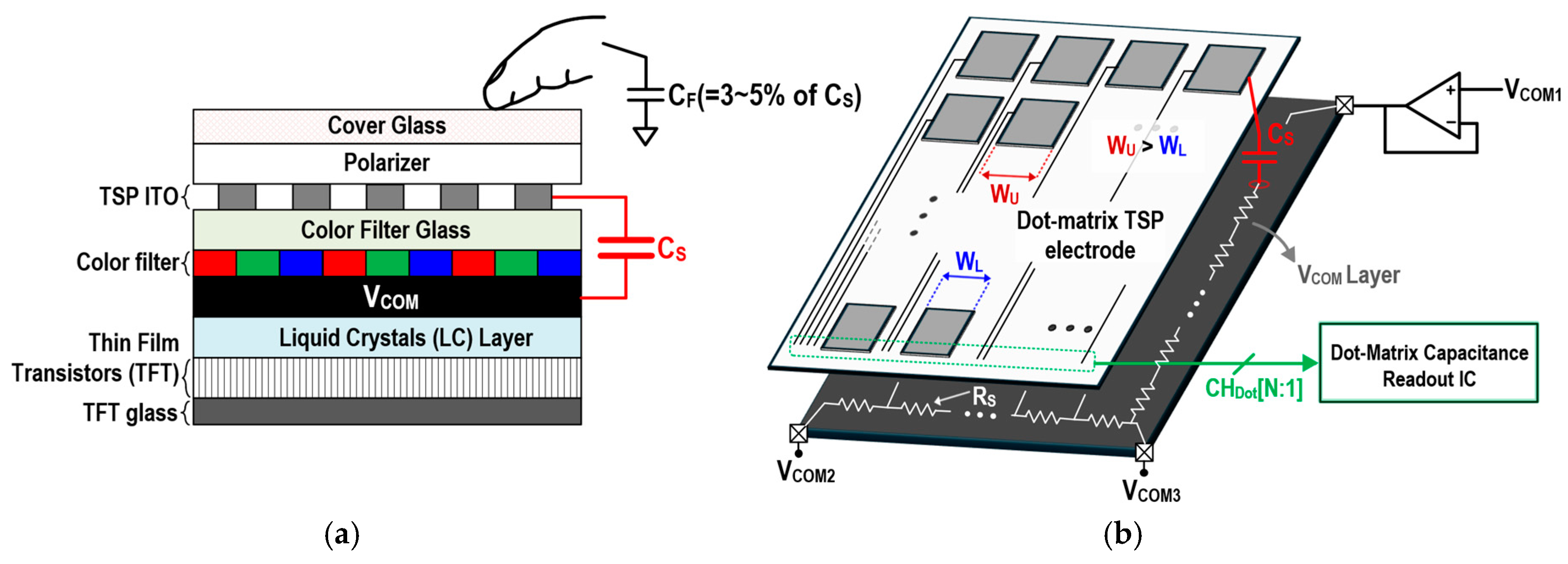
2. Proposed TSP Readout System

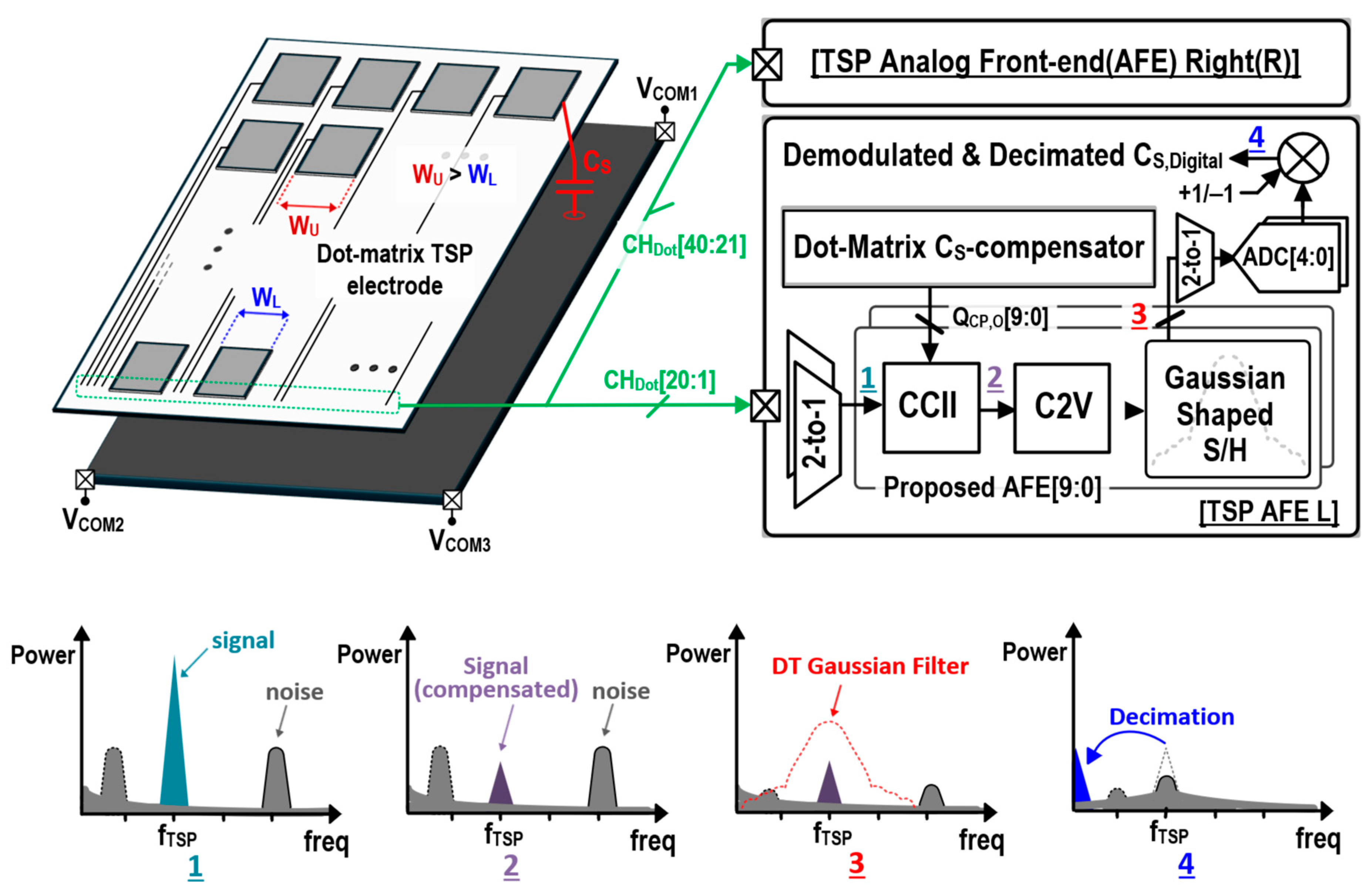
2.1. Whole System Architecture

The top of Figure 2 illustrates the proposed overall system architecture of the TSP sensing front-end. The sensing front-end is divided into two sections: TSP AFE Right (R), which handles dot-matrix TSP channels (CHDot [20:1]), and TSP AFE Left (L) for CHDot [40:21]. This division is essential due to the integration with the display driver IC (DDI) as a TDDI, centrally located within the system. Each front-end section comprises key functional blocks, including a 2-to-1 multiplexer, a second-generation current conveyor (CCII), a current-to-voltage converter (C2V), a sample-and-hold circuit (S/H), and an ADC. Additionally, a dot-matrix Cs-compensator is integrated and its output cells generate compensation charges of QCP,O [9:0] to each CCII input to effectively nullify the baseline Cs, ensuring accurate signal processing and minimizing capacitance nonuniformity.
First, the CCII converts the capacitance CS into current and amplifies it. The CCII’s inherent low-pass characteristics suppress high-frequency coupled noise. Simultaneously, the baseline Cs is nullified before current conversion, ensuring that only the capacitive variations from finger touch (CF) are transferred to the C2V for further processing. The subsequent C2V stage consists of an operational amplifier (op-amp) with a feedback integral capacitor (CINT) and resistor (RINT). The parallel combination of CINT and RINT converts the current from the CCII into a proportional voltage while introducing a high-pass pole at a low frequency. Consequently, the poles at the CCII input and the C2V output collectively form a band-pass filter centered at the TSP driving frequency (fTSP). The S/H functions as a voltage sampling circuit for subsequent analog-to-digital (A/D) conversion while incorporating a reconfigurable Gaussian filtering effect. Operating as a discrete-time (DT) circuit, the S/H can implement Gaussian coefficients using a discrete-level sampling capacitor array, synchronized with a clock operating at twice the frequency of fTSP.
The bottom of Figure 2 shows the frequency translation of the capacitance signal across each AFE stage, emphasizing the frequency range of the TSP signals and the dominant noise sources at each front-end stage. First, the capacitance-induced signal is up-modulated to fTSP to shift its frequency spectrum away from low-frequency noise sources, such as DC offsets from the charger and hum noise from power lines (50–60 Hz). Then, band-pass filtering within the AFE removes out-of-band noise, while the dot-matrix CS compensator isolates the capacitive change by finger (CF), ensuring accurate touch detection. After discrete-time Gaussian filtering in the sample-and-hold (S/H) and A/D conversion stages, demodulation is performed in the digital domain through +1/−1 coefficient multiplication. Since the +1/−1 multiplication is synchronized to twice the frequency of fTSP, intrinsic noise at the baseband, such as DC offset and 1/f noise, is up-modulated to fTSP during this process. The resulting noise components are then removed through decimation filtering, ensuring that only the desired baseband signal components (CS,Digital) are retained for further processing.

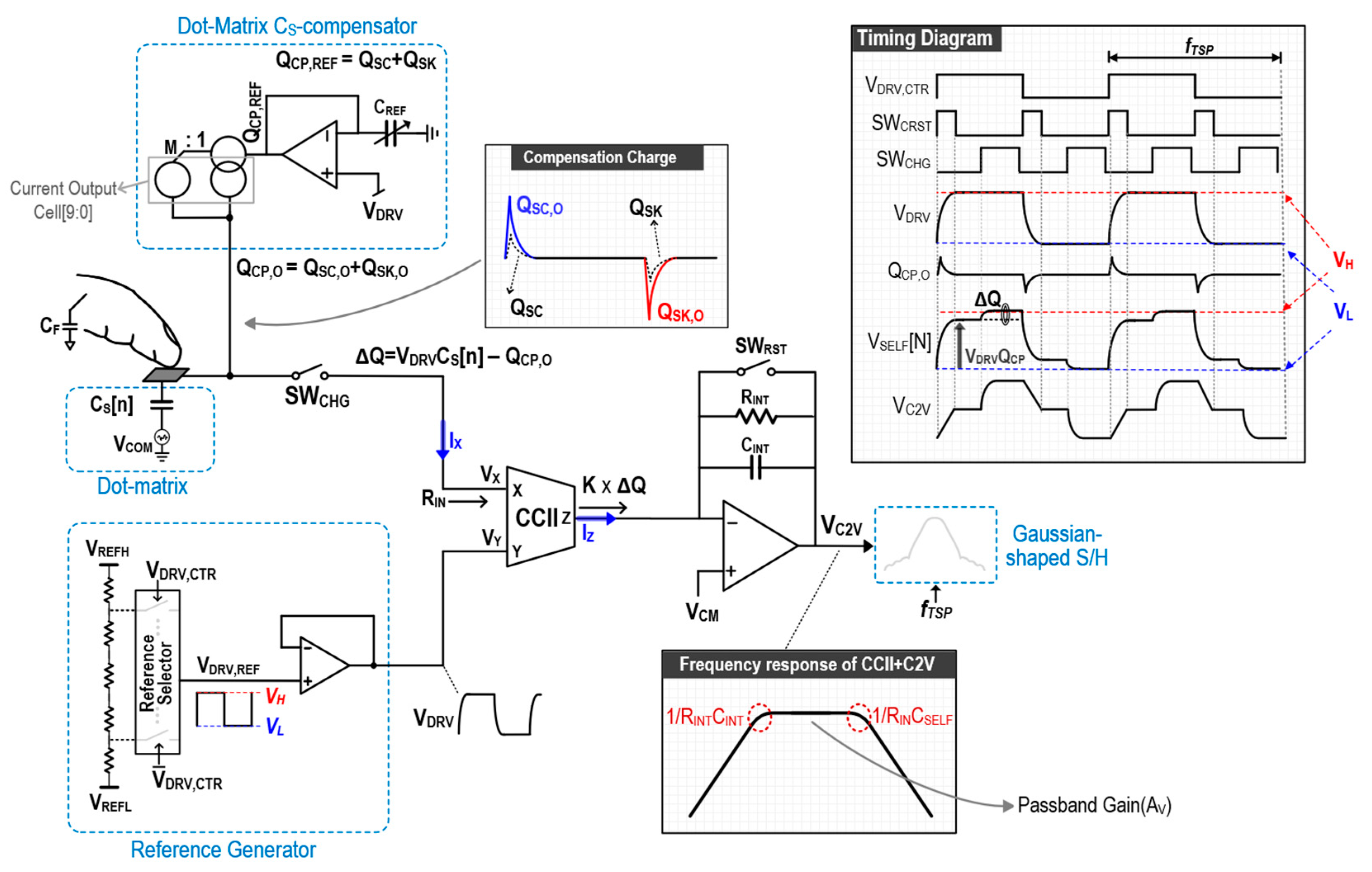
2.2. Sensing Front-End

Figure 3 illustrates the sensing front-end, consisting of a CCII and a C2V converter along with its timing diagram. The CCII, directly connected to the TSP electrode via SWCHG, has its X node (VX) referenced to the Y node voltage (VY). When VY is driven by an AC-modulated VDRV, VX achieves the same voltage level and drives CS[n] with virtual VDRV. The VDRV signal is generated by a unity-gain buffer and a resistor string in the reference generator, where VH and VL are alternately selected by VDRV,CTR to produce the AC-modulated VDRV. Another key feature of the CCII is its ability to copy the input current (IX) to the Z node (IZ) with a multiplication factor of K. Since CS[n] is driven by the virtual VDRV, a proportional charge of VDRV × CS[n] is generated and transferred to the X node as a current. However, due to the large CS[n] of the TSP electrode, the IZ (=K × IX) can saturate the subsequent front-end stage. To mitigate this, only the capacitive variation from CS[n], approximately corresponding to the CF of a finger, should be transferred to the next sensing stage. For this purpose, a dot-matrix CS-compensator is designed, with its output connected to CS[n]. Instead of fully transferring the charge of VDRV × CS[n], the static portion of CS[n] is eliminated by QCP,O. Since the charge of VDRV × CS[n] is modulated by fTSP, the proposed compensator alternately generates sinking (QSK,O) and sourcing (QSC,O) charges for effective compensation. Once the sampling switch (SWCHG) is closed, only the differential charge of ∆Q (=VDRV × CS[n] − QCP,O) is transferred. The charge of QCP,REF is generated by a metal–insulator–metal (MIM) reference capacitor (CREF) driven by virtual VDRV, while a current amplifier at the output boosts that current to QCP,O through fine and coarse tuning. The tuning ratio (M) can be reconfigured depending on the measurable channel-dependent size of CS[n].
To mitigate external noises, such as VCOM noise, the sensing front-end incorporates a bandpass filter (BPF). The charge conversion from CS[n] to IX at the CCII input generates a transfer function’s zero at DC. Conversely, the large parasitic capacitance combined with the input impedance of the CCII forms a high-frequency low-pass pole. The C2V converts this high-pass-filtered IZ to a proportional voltage. Simultaneously, RINT in parallel with CINT introduces a low-frequency high-pass pole, collectively shaping the bandpass filter response. The passband gain (AV) from VDRV to VC2V can be described by
A V = K ( C S n M × C R E F ) C I N T
where K is the current gain of CCII from the X node to the Z node, and M denotes the charge-boosting ratio of the dot-matrix CS-compensator, which can be reconfigured based on the size of CS[n]. The operation of C2V is synchronized with the switches SWRST and SWCHG as described in the timing diagram of Figure 3. When SWCHG is closed, the proportional charge is integrated on CINT, while SWRST resets CINT to prevent saturation of the front-end before the arrival of the next set of samples.

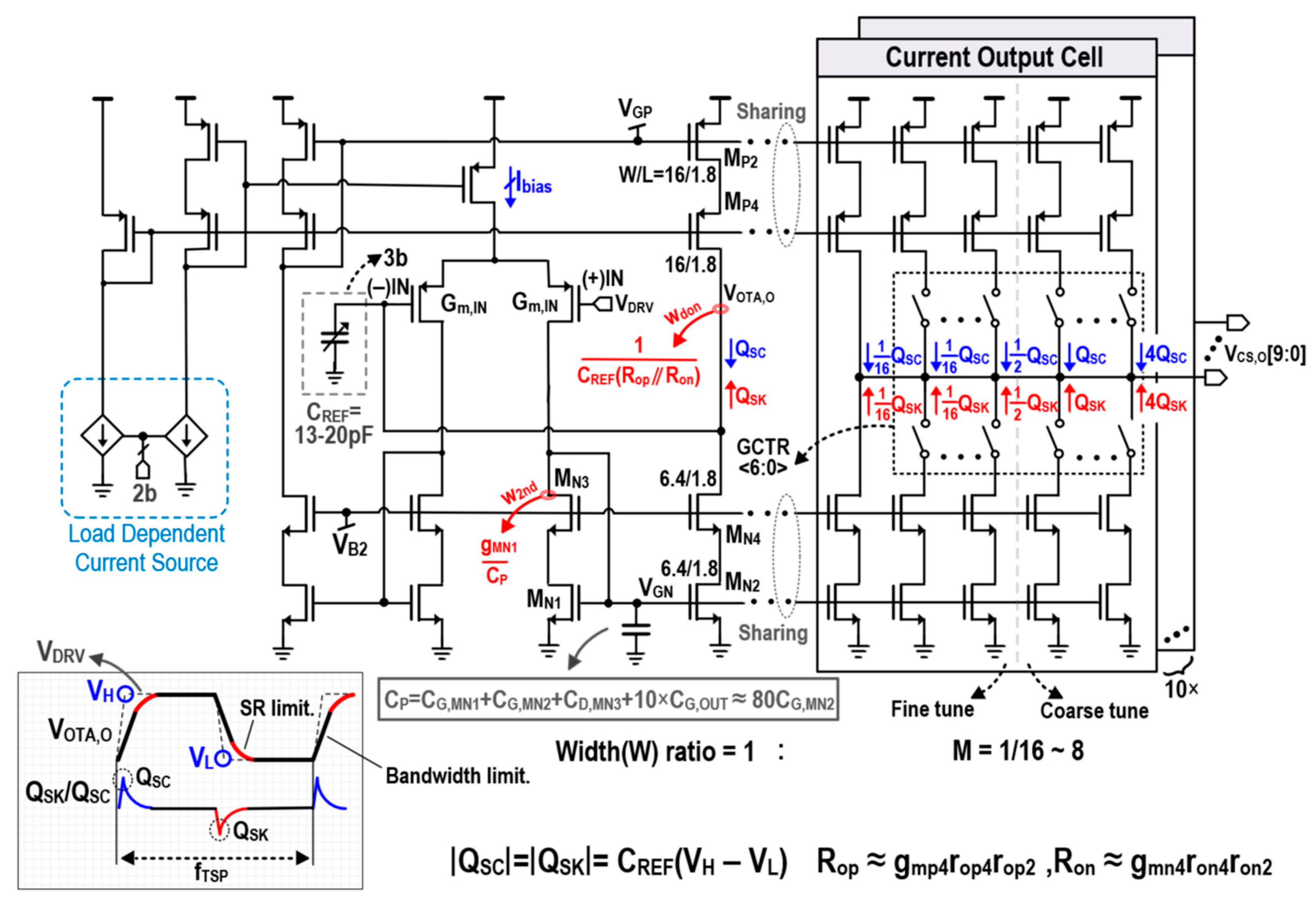
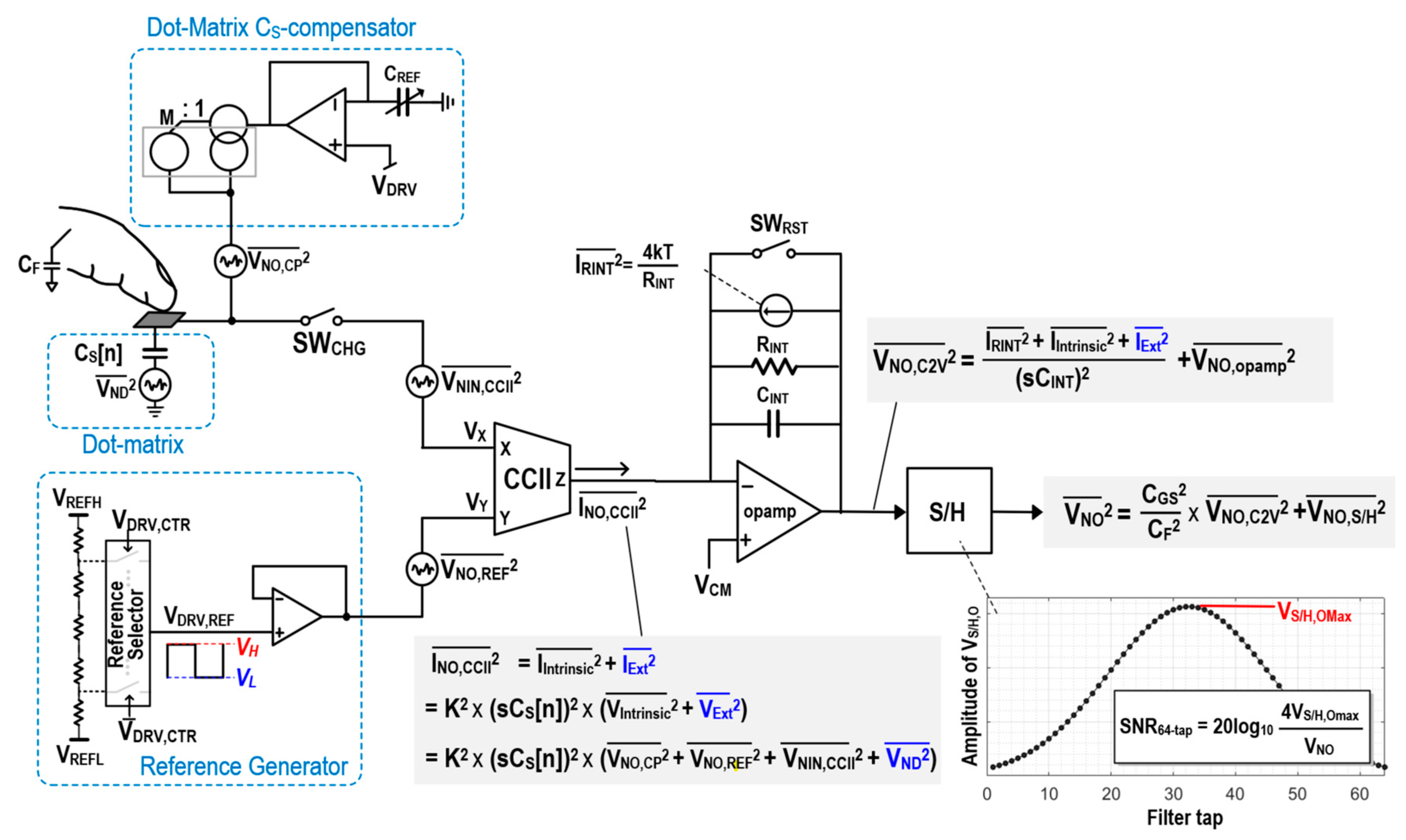
2.3. Dot-Matrix CS-Compensator

There have been numerous studies on self-capacitance (CS) sensing front-ends, with various compensation techniques proposed. The compensation using chip-integrated capacitors has been identified as one of the most accurate topologies, as demonstrated in [14]. However, this approach requires an increasing number and size of integrated capacitors proportional to the number of sensing channels, which significantly increases the chip area and makes it unsuitable for cost-sensitive applications. To address this, current-mode compensation schemes employing static sinking or sourcing currents have been utilized [15,16], offering an area-efficient solution for realizing the compensation charge. However, this method is highly susceptible to process and temperature variations. Temperature sensitivity presents a critical challenge in smartphone applications, where operational conditions are heavily affected by environmental factors, such as ambient weather variations.
The proposed CS-sensing circuit achieves a balance between accuracy and area efficiency by utilizing both integrated capacitors and a current-mode scheme. As shown in Figure 4, the compensator incorporates three main blocks: an integral reference capacitor (CREF), adjustable from 13 pF to 20 pF in 1 pF increments, connected to the negative input of the OTA (-)IN, an OTA configured as a unity-gain amplifier, which transfers charges from CREF (QSC, QSK) to its output, and 10 current output cells, which amplify QSC and QSK to compensate the channel-dependent CS. When the (+) input of the OTA, (+)IN is driven by the AC-modulated VDRV at a frequency of fTSP, CREF is alternately charged to VH or VL, delivering equivalent charges of QSC and QSK to the OTA’s output. The absolute variation in these charges is equal to CREF  × (VH − VL), which modulates the gate voltages (VGP and VGN) of the PMOS/NMOS transistors (MP2, MN2) in the current sources. Since the current copying output cell shares the VGN and VGP with the output of the OTA, it generates and amplifies CREF  × (VH − VL) at its output (VCS,O [9:0]) by ratio M to compensate for the baseline CS. This cell includes both a 4b fine compensation unit (1/16QSC to 1/2QSC) with 1/16QSC steps and a 3b coarse compensation unit (QSC to 4QSC) with QSC steps controlled by GCTR<6:0>. For instance, with a CREF of 20 pF, the compensation range for CS spans from 1.25 pF to 160 pF with a 7b resolution.
Although the OTA has a single dominant pole (wdon) at its output formed by CREF and PMOS/NMOS cascode resistors in parallel (Rop//Ron), its stability is degraded by parasitic capacitance from the 10 output cells connected to VGN and VGP in parallel. Since the size of each output current cell is approximately eight times that of OTA, the gate capacitance of each cell (CG,OUT) is also eight times that of MN2‘s gate capacitance (CG,MN2). Consequently, the total parasitic capacitance at VGN (CP) can increase by approximately 80 times compared to a conventional OTA of the same device size without output current cells. The second pole is given by the product of the inverse of the transconductance of MN1 (gMN1) and CP, as described in Figure 4. Thus, the maximum unity gain frequency of the CS compensator is limited to gMN1/CP, degrading the response time of the compensator. Another key factor in degrading the compensation speed is the slew rate limitation of the OTA. With the voltage swing of VDRV approaching 1 V (=VH − VL), a significant portion of the compensation time is dominated by the slewing condition. Thus, depending on the channel location and the resistance of its routing trace, the slew rate can be improved and adjusted through a 2b controlled bias current (Ibias) of the OTA’s input pairs (Gm,IN).

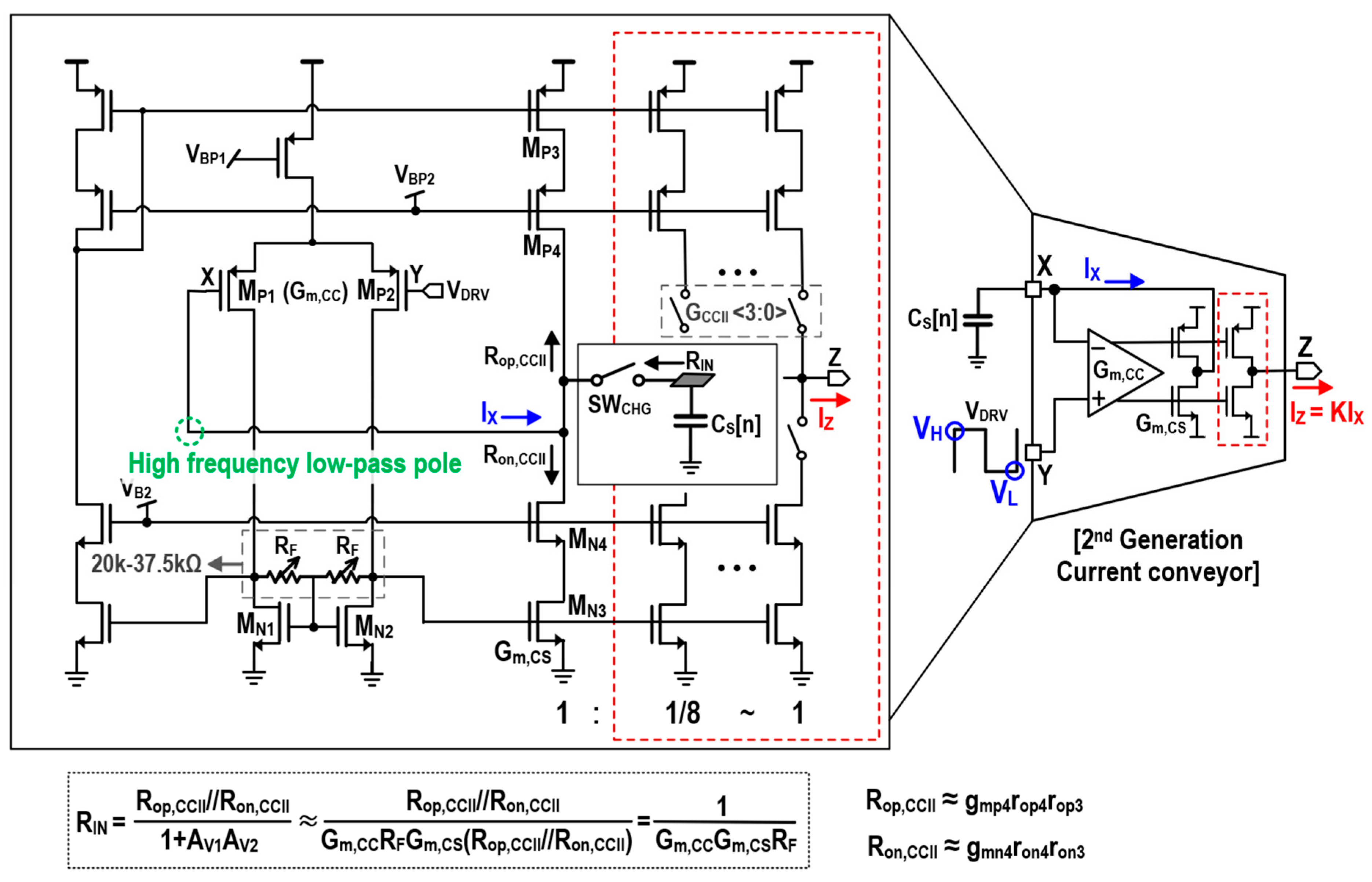
2.4. Proposed Second-Generation Current Conveyor (CCII)

The CCII at the sensing front-end serves two purposes in the readout system. First, it converts the capacitive variation at the TSP into proportional current. Second, it utilizes the parasitic capacitance of the TSP (CS[n]) to create a high-frequency low-pass pole, mitigating external noises. At the same time, the large CS[n], of the order of 100–200 pF should not limit the system’s bandwidth, aided by the small input resistance (RIN) of the CCII. Previously, various methods have been proposed to implement the CCII [17,18,19,20]. However, in this design, a negative-feedback closed-loop configuration is employed to effectively reduce the RIN of the CCII by the loop gain.
As shown in Figure 5, the OTA consists of two gain stages, with an additional resistor RF in the first stage to further enhance the overall gain. Since RF is significantly smaller compared to the channel resistances of the PMOS input pairs (MP1, MP2) and NMOS current source pairs (MN1, MN2), the gain of the first stage (AV1) is determined by the product of the input transconductance of MP1 and MP2 (Gm,CC) and RF [7]. The second gain stage (AV2) is determined by the transconductance Gm,CC of MN3 and the parallel combination of the PMOS and NMOS cascode resistances (Rop,CCII//Ron,CCII). When unity-gain feedback is applied, the effective cascode resistance is reduced by the product of AV1 and AV2. With RF tunable between 20 kΩ to 37.5 kΩ using 3b control and Gm,CS designed to be 150 μS, the reduction factor in RIN by the additional gain stage ranges from 3 to 5.625, depending on the actual panel loading. The current amplification ratio (from IX to IZ) is adjusted from 1/8 to 15/8 to prevent saturation of the subsequent C2V and Gaussian-shaped S/H circuit.

2.5. Sensing Back-End

Although a filtering effect is implemented in the sensing front-end using CCII and C2V, which performs bandpass filtering to mitigate external noise, the noise environment can be varied in modern commercial mobile devices. In particular, the VRR driving in the DDI necessitates a more systematic adaptive filtering approach in the TSP readout system. The sensing back-end comprises a Gaussian-shaped sample and hold (S/H) circuit, and a successive approximation register (SAR) ADC. The Gaussian-shaped S/H circuit features both a discrete-time (DT) finite impulse response filter (FIR) effect and voltage sampler for A–D conversion by successively sampling the output of C2V onto the reconfigurable sampling capacitor CGS, as shown in Figure 6. The CGS is composed of 15 unit capacitors CGS,u [14:0] to enhance matching accuracy, with their values continuously increasing and decreasing in a Gaussian-shaped manner synchronized to twice the frequency of fTSP. The operating timing diagram and the schematic of the Class AB op-amp are also presented in Figure 6. First, the control signal VS and VS,Pre are applied to input and feedback switches during the sampling phase. In this phase, the output (VS/H,O) is maintained at half the supply voltage (=VCM) due to the unity-gain feedback configuration, while VC2V is sampled on the left-side plate of CGS. After disabling VS,Pre and then VS to eliminate input-dependent charge injection, the sampled charge on CGS is transferred to CF, generating an output of VC2V × (CGS/CF). Since CGS varies in each S/H phase, the generated output level VS/H,O is adjusted according to the Gaussian coefficients gains GGCTR [14:0] applied to CGS, effectively implementing a DT FIR filter of the digital signal processor (DSP) in the analog signal. Therefore, when GGCTR [14:0] reaches its maximum value 0 × 7FFF, the S/H gain is maximized with all CGS,U enabled, and subsequently decreases to its minimum within the scan-time. The scan time is determined by the product of twice the inverse of fTSP and the number of Gaussian filter coefficients (NGauss).
The primary goal of implementing Gaussian filtering in the analog domain is to achieve an area- and power-efficient solution compared to its digital counterpart. However, as the number of Gaussian coefficient levels increases, the design complexity in the analog domain also rises. Therefore, a careful trade-off must be made to balance efficiency and complexity. Figure 7a illustrates the frequency response based on the Gaussian coefficient quantization levels, comparing the results from 4-bit (4b) and 7-bit (7b) discrete Gaussian levels with a continuous-time (CT) Gaussian waveform. In 4b quantization, the filter coefficients range from −7 to 7, while in 7b quantization, the range extends from −63 to 63, offering improved approximation of the continuous-time Gaussian waveform at the cost of increased implementation complexity. Here, the TSP driving frequency fTSP is set to 200 kHz, with the number of filter taps set to 64, resulting in 160 μs scan-time. The bandwidth within the main lobe frequency is measured to 40 kHz, which remains consistent across all three cases. However, the external noise immunity at 1.4 times the main frequency (=200 kHz), or the sideband ripple in the 4b quantization, is degraded by 16.4 dB compared to the ideal CT Gaussian waveform. This issue can be mitigated using the previously mentioned analog BPF, which is implemented with a CCII and C2V, making the 4-bit design a practical trade-off between performance and complexity. Figure 7b also illustrates the bandwidth modification as a function of the number of filter taps. While the bandwidth can be adjusted based on external noise conditions, this comes at the cost of increased scan time, which must be considered depending on the operating environment.

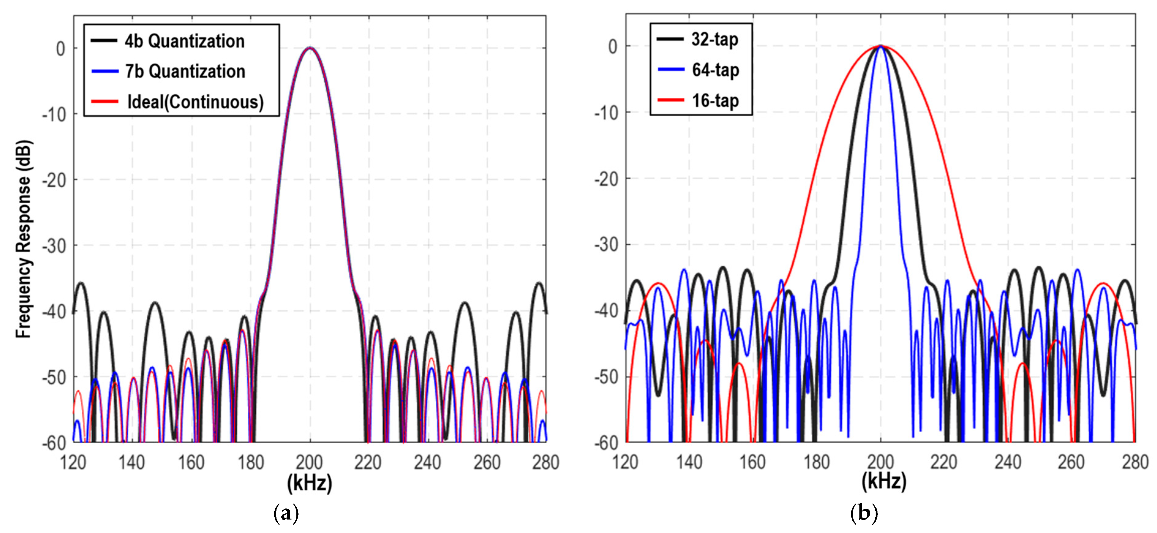
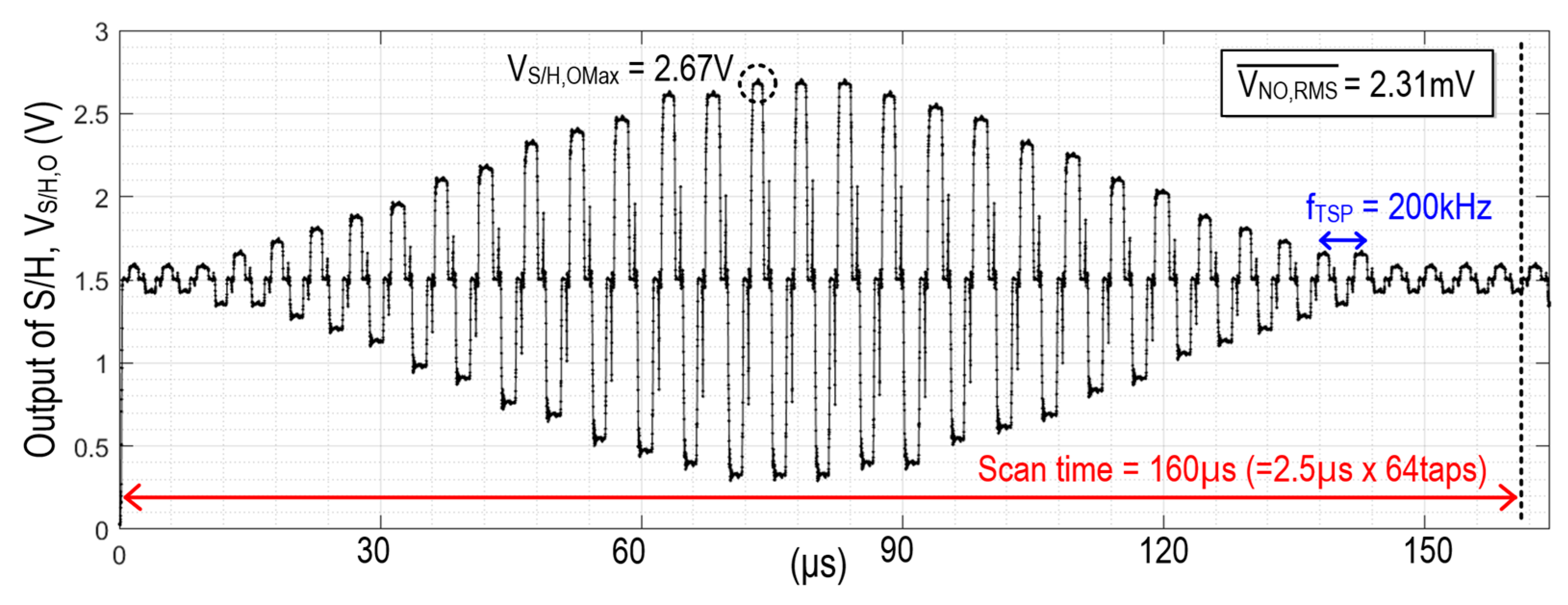
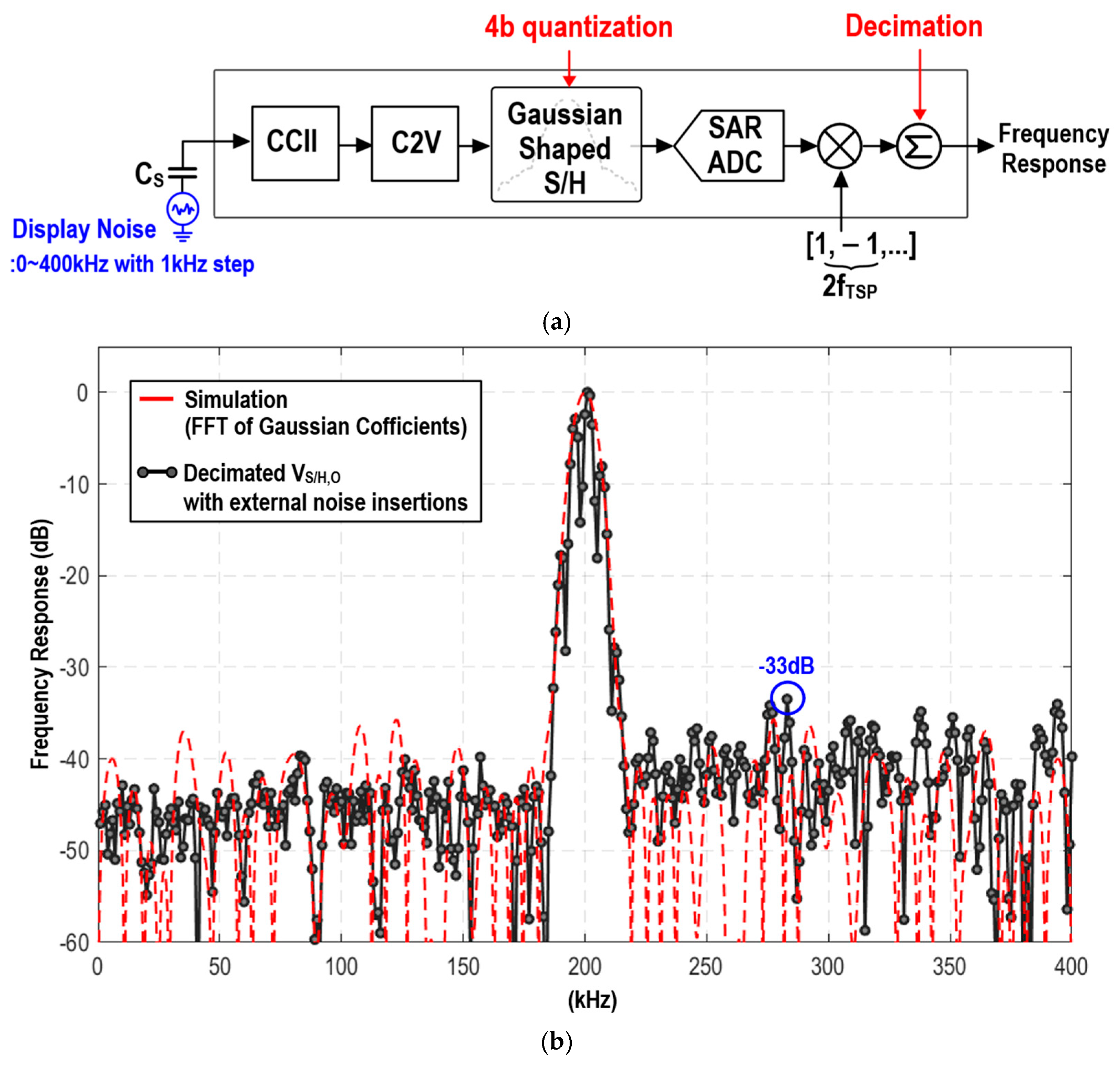
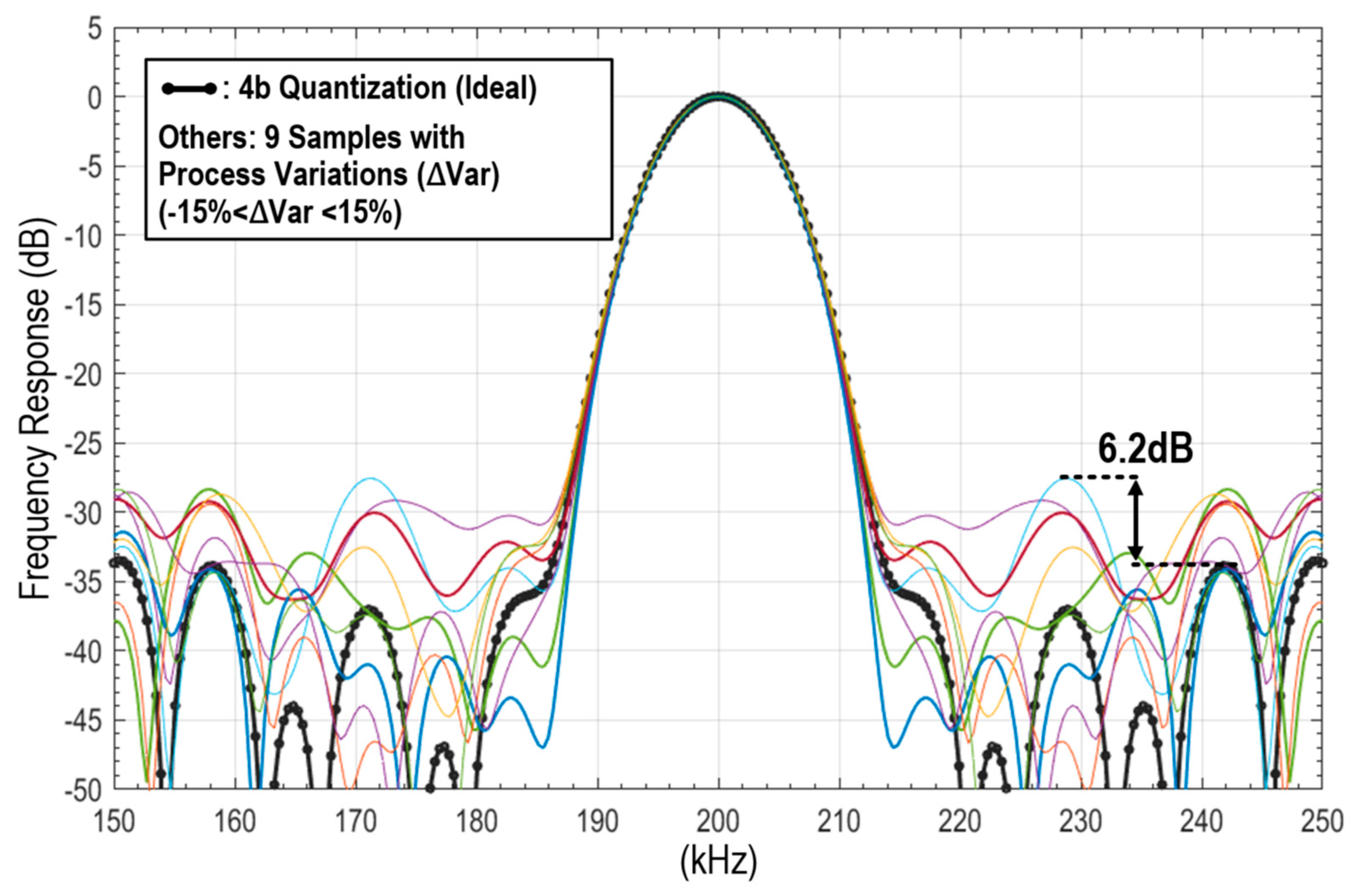
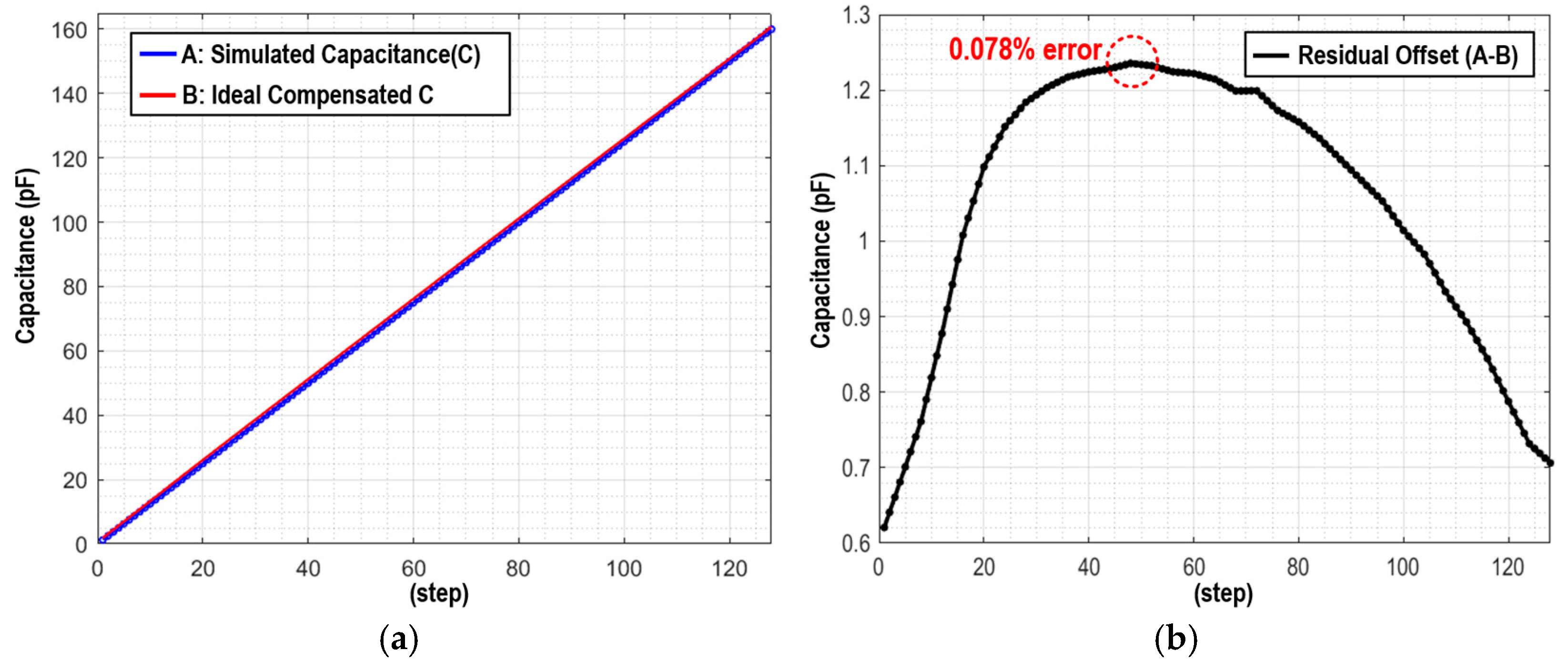
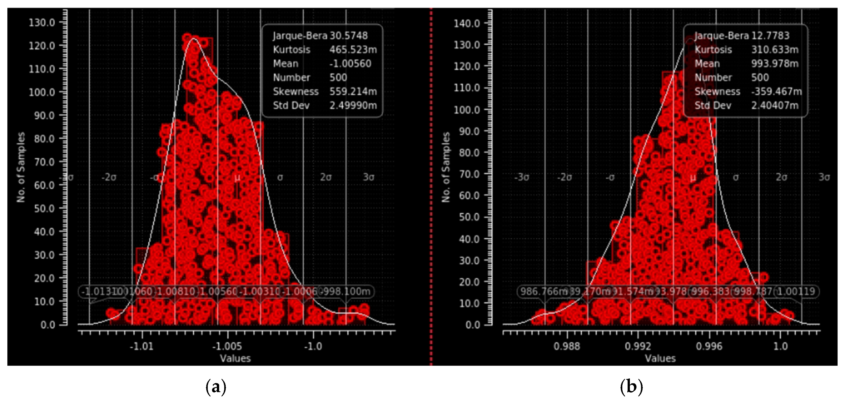
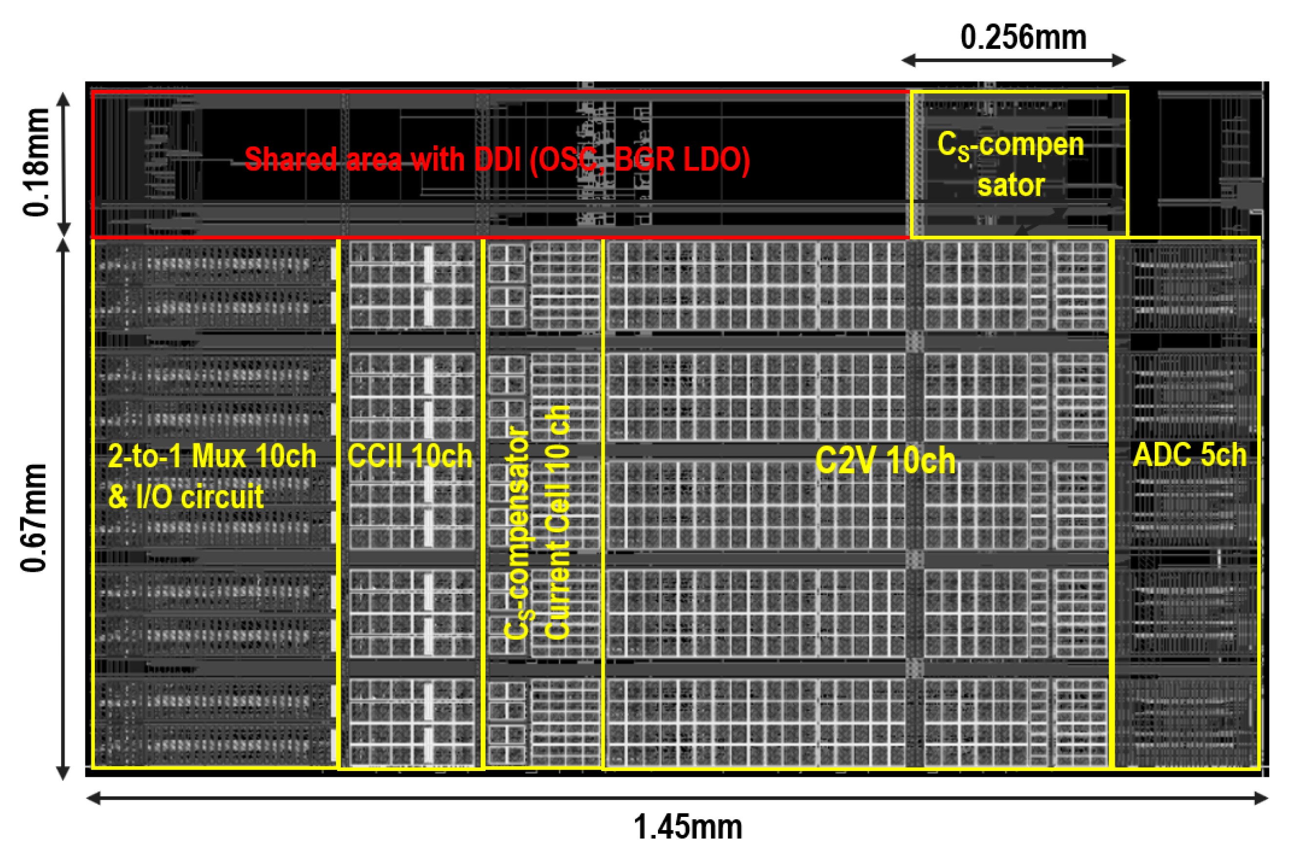
3. Simulation Results

To define the sensitivity requirements for the sensing front-end, the intrinsic circuit noise and external noise are analyzed. Although this study primarily presents simulation results rather than measurement data, the proposed simulation methodology can be utilized to define system specifications and provide practical design guidelines. Moreover, this approach is not limited to the proposed system but can be adapted to other sensing front-end structures, enhancing its applicability.
Figure 8 shows the overall AFE architecture, incorporating both intrinsic and external noise power within the system. The output-referred noise voltages for the CS-compensator, reference generator, op-amp in C2V, and Gaussian-shaped S/H circuits are represented as V N O , C P 2 ¯ , V N O , R E F 2 ¯ , V N O , o p a m p 2 ¯ , and V N O , S / H 2 ¯ while the input-referred noise voltage of the CCII is V N I N , C C I I 2 ¯ and the noise current of the feedback resistor in the C2V is I R I N T 2 ¯ . Additionally, the external noise from the capacitive coupling is denoted as V N D 2 ¯ . Thus, the overall noise at the AFE output or S/H output is expressed as V N O 2 ¯ , as also depicted in Figure 8. However, its amount cannot be quantified due to its dependence on the environmental noise condition. Thus, we define two evaluation metrics: one to qualify the SNR over the intrinsic circuit noise, and the other to assess noise immunity against the external noise by measuring the system’s responsiveness to noise frequencies ranging from DC to a predefined high frequency. First, the intrinsic SNR can be described [21] in Equation (2)
S N R   ( d B ) = 20 l o g 10 N F i l t e r × V S / H , O M a x 2 V N O ¯
where NFilter is the number of filter taps, which is twice the number of TSP driving, and VS/H,OMax and V N O ¯ are the maximum output voltage level and the total output-referred noise observed at the Gaussian-shaped S/H circuit, respectively. Since the signal power from capacitive changes is proportional to NFilter, and the noise power is proportional to the square root of NFilter, the SNR becomes proportional to the square root of NFilter, indicating that a higher SNR can be achieved with increased scan time. Moreover, the factor of 2 in the denominator of Equation (2) reflects the reduction in the total signal amplitude due to Gaussian shaping in the S/H circuit, compared to maintaining a constant VS/H,OMax at the output. We target an intrinsic SNR exceeding 60 dB with a 1 pF capacitive variation from a finger (CF), NFilter = 64 Gaussian filter coefficients, and a 200 kHz TSP driving fre- quency. Figure 9 shows the simulated output (VS/H,OMax) of the Gaussian S/H circuit. The output root mean square (RMS) integrated noise of the S/H circuit over the system bandwidth was also evaluated using the noise simulation function in Virtuoso. The VS/H,OMax reaches up to 2.67 V at the center of the Gaussian-shaped output, achieving a signal voltage of 1.17 V for capacitive change (VS/H,OMax-VCM), while the simulated output RMS noise ( V N O , R M S ¯ ) is 2.31 mV, resulting in an intrinsic SNR of 54 dB in a single pulse. With NFilter of 64 and a 200 kHz TSP driving frequency, the SNR is further enhanced to 66 dB within a scan time of 160 μs. As the TSP frame rate is typically synchronized with the display in TDDI, the reduced scan time enhances system efficiency by maximizing the time allocated to display driving. For instance, with a 120 Hz display refresh rate (8.33 ms per frame), apart from the 160 µs scan time, the remaining 8.17 ms can be fully utilized for display driving, allowing the TSP to remain in idle mode, thereby improving the overall power efficiency.
Secondly, as shown in Figure 10, external noise immunity was simulated by sweeping the external noise ( V N D 2 ¯ in Figure 8) from DC to 400 kHz in 1 kHz steps and injecting through CS[n]. To verify the discrete-time Gaussian filter response, the ADC output was demodulated using discrete signals of [1, −1] after A–D conversion and then decimated to DC to obtain the raw value at each display noise frequency. Compared to the FFT results obtained directly from the 64-tap Gaussian filter coefficients, the simulated noise performance under the noise sweep exhibits a high level of consistency, achieving −33 dB noise rejection at 278 kHz. To evaluate the impact of process variation on the filter response, the metal–insulator–metal (MIM) capacitor in the chip is assumed to vary by ±15% variation (∆Var) of its nominal value. Consequently, CGS,u in the Gaussian S/H circuit experiences the same variation. Figure 11 compares the Gaussian filter responses obtained from ideal 4-bit quantized filter coefficients and those affected by ±15% random variations in CGS,u. In the worst case, where CGS,u exhibits a ±15% random mismatch across all nine samples, the attenuation capability degrades by 6.2 dB. However, since CGS,u is placed in close proximity within the same location, the impact of its random mismatch will be further mitigated in practice.
Figure 12 shows the simulated results of the CS compensator’s compensation linearity, where the reference capacitor CREF is set to 20 pF, and the current gain (M), corresponding to the compensation capacitance, increases from 1/16 (1.25 pF) to 8 (160 pF) across a 7-bit range. The maximum capacitive error occurs at the midband of the compensation range, reaching 1.24 pF, which corresponds to a 0.078% error in the total 160 pF compensation range. To verify the impact of process variation on the compensation accuracy, the mismatch between source (QSC) and sink (QSK) compensation charges was analyzed using Monte Carlo simulations in the virtuoso tool, with CREF ideally fixed, as shown in Figure 13. In the simulation, 500 deviation samples were obtained to evaluate the statistical distribution of compensation charge variations, while the results of QSK in (b) were scaled by the mean value of QSC to facilitate a direct comparison of their absolute value differences. The width and length of NMOS (MN2, MN4) and PMOS (MP2, MP4) cascode current sources are specified in Figure 4, with dimensions scaled in micrometers. With the aid of large channel length (=1.8 μm), the standard deviation was measured as 0.25% for QSC and 0.24% for QSK, while the difference between QSC and QSK is 1.2%, demonstrating high compensation accuracy.
Figure 14 shows the layout of the sensing front-end designed for 20 dot-matrix sensor electrodes, comprising 10 front-end blocks and 5 SAR ADCs. The CS compensator is positioned at the top of the layout, with the adjacent area allocated for general analog blocks, such as the LDO, BGR, and OSC, which will be shared by the display driver IC. The total front-end area is double the 1.017 mm2 for 40 dot-matrix sensors, CHDot [40:1]. Table 1 summarizes the front-end performance compared to previous TDDI circuit designs. Compared to previous works, the proposed IC operates with a single supply voltage of 3.3 V, allowing the PMIC to power the controller IC using a single voltage rail. This design enhances both implementation and area efficiency, as it requires only a single bypass capacitor on the 3.3 V supply pin, thereby minimizing the PCB footprint in compact smartphone designs. It also achieves a high scan rate of 3.125 kHz for 40 TSP electrode sensing, which is advantageous in TDDI designs, as TSP and DDI operate sequentially in a time-division manner. The 40 TSP electrodes correspond to a display size of 1.91 inches, assuming a channel pitch of 4.5 mm, making it suitable for wearable device panels. With the aid of a channel-dependent CS-compensator featuring independent fine and coarse tuning, the system can accommodate various TSP shapes that exhibit location-dependent CS variations.
Although a fair comparison with previous studies presenting measurement results is not feasible, the proposed design demonstrates superior area efficiency with 0.05 mm2 AFE area per sensor electrode and enhanced noise immunity using an analog Gaussian filter in the DT S/H circuit.

4. Conclusions

This work presents an analog Gaussian-shaped filter and a current mode compensation technique for dot-matrix TSP readout systems, addressing critical challenges in noise immunity and area efficiency for in-cell touch and display integrated panels. The proposed system achieves an intrinsic SNR of 66 dB with a 200 kHz TSP driving frequency and a scan time of 160 μs. Additionally, the 4-bit quantized Gaussian filter provides −33 dB noise suppression at 278 kHz, effectively mitigating out-of-band noise.
The CS compensator demonstrates high linearity, with a maximum capacitive error of 1.24 pF, corresponding to a 0.078% deviation across a 7-bit range. The system achieves a simulated power consumption of 24 mW and an area efficiency of 0.05 mm2 per sensor electrode, demonstrating feasibility for mass production.
While the evaluation is based on simulation results, the proposed methodology establishes a practical framework for system specification and design optimization. Furthermore, the methodology is versatile and can be extended to other circuit designs. The combination of an analog Gaussian filter and current mode compensation offers a scalable, area-efficient, and noise-immune solution for modern TSP readout systems, making it well suited for integration into cost-sensitive mobile devices.

Funding

This research received no external funding.

Institutional Review Board Statement

Not applicable.

Informed Consent Statement

Not applicable.

Data Availability Statement

Data are contained within the article.

Acknowledgments

This work was supported by the Research Resettlement Fund for the new faculty of Kwangwoon University in 2021 and has been conducted under the Research Grant of Kwangwoon University in 2023.

Conflicts of Interest

The author declares no conflicts of interest.

References

  1. Kim, K.D.; Byun, S.H.; Choi, Y.K.; Baek, J.H.; Cho, H.H.; Park, J.K.; Ahn, H.Y.; Lee, C.J.; Cho, M.S.; Lee, J.H.; et al. A Capacitive Touch Controller Robust to Display Noise for Ultrathin Touch Screen Displays. In Proceedings of the IEEE International Solid-State Circuits Conference, San Francisco, CA, USA, 19–23 February 2012. [Google Scholar]
  2. Seo, J.; Nam, H. Low power and low noise shift register for in-cell touch display applications. IEEE J. Electron. Devices Soc. 2018, 6, 726–732. [Google Scholar] [CrossRef]
  3. Kim, C.; Lee, D.S.; Kim, J.H.; Kim, H.B.; Shin, S.R.; Jung, J.H.; Song, I.H.; Jang, C.S.; Kwon, K.S.; Kim, S.H.; et al. Advanced In-cell Touch Technology for Large Sized Liquid Crystal Displays. Dig. Tech. Pap. Int. Symp. SID 2015, 46, 895–898. [Google Scholar] [CrossRef]
  4. Lee, S.H.; An, J.S.; Hong, S.K.; Kwon, O.K. In-cell Capacitive Touch Panel Structures and Their Readout Circuits. In Proceedings of the International Workshop on Active-Matrix Flat panel Displays and Devices, Kyoto, Japan, 6–8 July 2016; pp. 258–261. [Google Scholar]
  5. Byun, S.H.; Lee, H.; Song, T.G.; Lee, J.; Baek, J.; Ha, G.; Baek, S.; Kim, Y.; Jung, W.G.; Lim, H.W.; et al. A 45.8 dB-SNR 120 fps 100 pF-Load Self-Capacitance Touch-Screen Controller with Enhanced In-Band Common Noise Immunity Using Noise Antenna Reference. In Proceedings of the IEEE International Solid-State Circuits Conference, San Francisco, CA, USA, 19–23 February 2023. [Google Scholar]
  6. An, J.Y.; Choi, S.H.; Kim, S.W.; Lee, J.Y.; Lee, H.M.; Choi, Y.K. Noise Immunity in Capacitive Sensing: Single-Ended AFE Design with Common-Current Subtraction for Mutual- and Self-Capacitance Sensing in 390pF Load. In Proceedings of the IEEE International Solid-State Circuits Conference, San Francisco, CA, USA, 19–23 February 2024. [Google Scholar]
  7. Lee, J.; Ham, J.; Lee, H.; Jang, W.; Kim, H.; So, B.; Ko, S. A 620 pF-Compensated Dual-Mode Capacitance Readout IC for Sub-Display TSP with VRR Scan. In Proceedings of the IEEE International Solid-State Circuits Conference, San Francisco, CA, USA, 18–22 February 2024. [Google Scholar]
  8. Yang, J.-H. A highly noise-immune touch controller using filtered-delta-integration and a charge-interpolation technique for 10.1-inch capacitive touch-screen panels. In Proceedings of the IEEE International Solid-State Circuits Conference, San Francisco, CA, USA, 19–23 February 2013. [Google Scholar]
  9. Shin, H.; Ko, S.; Jang, H.; Yun, I.; Lee, K. A 55 dB SNR with 240Hz frame scan rate mutual capacitor 30 × 24 touch-screen panel read-out IC using code-division multiple sensing technique. In Proceedings of the IEEE International Solid-State Circuits Conference, San Francisco, CA, USA, 19–23 February 2013. [Google Scholar]
  10. Park, J.E.; Lim, D.H.; Jeong, D.K. A reconfigurable 40-to-67 dB SNR, 50-to-6400 Hz frame-rate, column-parallel readout IC for capacitive touch-screen panels. IEEE J. Solid-State Circuits 2014, 49, 2305–2318. [Google Scholar] [CrossRef]
  11. Kim, K.D.; Kang, S.; Choi, Y.K.; Lee, K.H.; Lee, C.H.; Lee, J.C.; Choi, M.; Ko, K.; Jung, J.; Park, N.; et al. A fully-differential capacitive touch controller with input common-mode feedback for symmetric display noise cancellation. In Proceedings of the 2014 Symposium on VLSI Circuits Digest of Technical Papers, Honolulu, HI, USA, 10–13 June 2014. [Google Scholar]
  12. SAMSUNG Display, Samsung Display Commercializes New, Variable Refresh Rate Technology for Increasing Smartphone Power Savings. Available online: https://news.samsung.com/us/samsung-display-commercializes-new-variable-refresh-rate-technology-for-increasing-smartphone-power-savings-galaxy-note20/?utm_source=chatgpt.com (accessed on 26 December 2024).
  13. Hotelling, S.; Christie, I.; Chaudhri, I. Multipoint Touch Surface Controller. U.S. Patent 8,279,180, 2 October 2012. Available online: https://patents.google.com/patent/US8279180B2/en (accessed on 26 December 2024).
  14. Hwang, H.; Lee, H.; Han, M.; Kim, H.; Chae, Y. A 1.8-V 6.9-mW 120-fps 50-Channel Capacitive Touch Readout with Current Conveyor AFE and Current-Driven ΔΣ ADC. IEEE J. Solid-State Circuits 2017, 53, 204–218. [Google Scholar] [CrossRef]
  15. Ko, S.H.; Yang, B.D. An Ultra-Compact Low Power Self-Capacitive Touch Screen Readout IC Embedding Reconfigurable Noise Immunity and Current-Driven Capacitance Compensation. IEEE Trans. Circuits Syst. II Express Briefs 2018, 66, 1321–1325. [Google Scholar] [CrossRef]
  16. Lee, J.; Ham, J.; Jang, W.; Lee, H.; Oh, J.; Goo, S.; Ko, S. A 145 − μW Always-on Touch Screen Readout and Always-on Haptic Driver IC for 1.26-Inch Circular Display of Wearable Device. In Proceedings of the 2023 IEEE SENSORS, Vienna, Austria, 29 October–1 November 2023. [Google Scholar]
  17. Kumar, S.; Kumar, N. Analysis of CMOS Second Generation Current Conveyors. Int. J. Eng. Res. Technol. 2014, 3, 947–953. [Google Scholar]
  18. Singh, P.; Sharma, A. A New CMOS Design and Analysis of Current Conveyor Second Generation (CCII). Int. J. Sci. Res. 2021, 6, 42–48. [Google Scholar]
  19. Minaei, S.; Yuce, E. New CMOS Current-Controlled Second Generation Current Conveyors. IEEE Trans. Circuits Syst. II Exp. Briefs 2008, 55, 1265–1269. [Google Scholar]
  20. Rathod, N.; Sharma, A. Design and Implementation of Different Generations of Current Conveyor Using 100 nm CMOS Technology. Int. J. Res. Dev. Eng. Technol. 2021, 2, 214–221. [Google Scholar]
  21. Park, S.H.; Kim, H.S.; Bang, J.S.; Cho, G.H.; Cho, G.H. A 0.26-nJ/node, 400-kHz Tx driving, filtered fully differential readout IC with parasitic RC time delay reduction technique for 65-in 169 97 capacitive-type touch screen panel. IEEE J. Solid-State Circuits 2017, 52, 528–542. [Google Scholar] [CrossRef]
  22. Jang, H.; Shin, H.; Lee, J.; Yoo, C.; Chun, K.; Yun, I. A 51 dB SNR 120 Hz Scan Rate 32 × 18 Segmented-VCOM LCD In Cell Touch-Display-Driver IC with 96-Channel Compact Shunt-Sensing Self-Capacitance Analog Front-End. In Proceedings of the IEEE International Solid-State Circuits Conference, San Francisco, CA, USA, 16–20 February 2020. [Google Scholar]
  23. Lee, H.; Ham, J.; Lee, J.; Jang, W.; Ko, S. A 620-pF-Compensated Dual-Mode Capacitance Readout IC for Subdisplay Panel Applications. IEEE Solid-State Circuits Lett. 2024, 7, 195–198. [Google Scholar] [CrossRef]
Figure 1. (a) Stack-up of an in-cell LCD display panel and (b) a conceptual diagram of a dot-matrix self-capacitance (CS) touch screen panel.
Applsci 15 01845 g001
Figure 2. Proposed dot-matrix TSP analog front-end (AFE) architecture with frequency range of TSP signal and noise across the LCD display.
Applsci 15 01845 g002
Figure 3. Circuit diagram of the TSP sensing front-end, its timing diagram, and frequency response of the second-generation current conveyor + capacitance-to-voltage converter.
Applsci 15 01845 g003
Figure 4. Circuit diagram of the proposed CS-compensator with an illustration of factors contributing to response time degradation.
Applsci 15 01845 g004
Figure 5. Circuit diagram of the second-generation current conveyor (CCII).
Applsci 15 01845 g005
Figure 6. Circuit diagram and operating timing diagram of Gaussian-shaped S/H circuit.
Applsci 15 01845 g006
Figure 7. Comparison of frequency responses: (a) 4b and 7b discrete Gaussian-shaped amplitude levels versus a continuous-time (CT) Gaussian waveform, and (b) impact of filter tap count (16, 32, 64 taps) on frequency response with a 4-bit quantized amplitude level.
Applsci 15 01845 g007
Figure 8. Analysis of intrinsic and external noise sources in the readout system.
Applsci 15 01845 g008
Figure 9. Simulated transient output waveform of Gaussian-shaped S/H circuit (VS/H,O) in 64-tap Gaussian filter coefficient scan time.
Applsci 15 01845 g009
Figure 10. (a) Simulation setup with display noise insertion from DC to 400kHz and (b) Comparison of external noise immunity: simulation results with noise frequency sweep and FFT results of 64-tap Gaussian coefficients.
Applsci 15 01845 g010
Figure 11. Frequency response comparison of a 64-tap Gaussian filter: CGS process variations in the S/H circuit (9 samples) vs. ideal 4-bit quantized coefficients.
Applsci 15 01845 g011
Figure 12. Simulated results of the CS compensator’s compensation linearity: (a) Ideal and simulated results across the 0–160 pF range, and (b) their differences.
Applsci 15 01845 g012
Figure 13. Monte Carlo standard deviation simulation results for (a) Cs-compensator’s source charge (QSC) and (b) sink charge (QSK) scaled by mean value of (a).
Applsci 15 01845 g013
Figure 14. Layout of the sensing front-end for the proposed system.
Applsci 15 01845 g014
Table 1. Performance summary and comparison with the state of the art.
This Work[5][15][22][23]
Process350 nm CMOS1.1 V/3.3 V/8 V/20 V
45 nm
130 nm/350 nm CMOS1.2 V/6 V/32 V
80 nm
130 nm/350 nm CMOS
CapacitanceDot-matrix
self-capacitance
Dot-matrix
self-capacitance
Dot-matrix
self-capacitance
Dot-matrix
self-capacitance
2-layered self- and mutual capacitance
Electrode40 dotsN/A16576 dots37
Sensor40216169637
AFE Area1.017 mm2 × 227.7 mm20.128 mm25 mm22.81 mm2
AFE Area/Sensor0.05 mm20.12 mm20.08 mm20.05 mm20.086 mm2
Power24 mW166 mW1.04 mW16 mW22.4 mW
Supply3.3 V1.1 V/3.3 V/5 V/6.6 V3.3 V1.2 V/6 V/32 V3.3 V
Scan Rate3.125 kHz120 Hz330 Hz120 Hz1.05 kHz for CS
Noise-removing schemeDiscrete-time Gaussian filter + BPFNoise antenna referenceMoving average + pseudo-random spreading of orthogonal drivingMoving average schemeNoise-monitoring scheme
SNR66 dB/1 pF
(simulation) (1)
45.8 dB/500 fF47.2 dB 51   dB / 7 Φ 36.1 dB
for 340 pF CS
(1) Since this study is based on simulation results, a direct and fair comparison with measurement-based results is not feasible.
Disclaimer/Publisher’s Note: The statements, opinions and data contained in all publications are solely those of the individual author(s) and contributor(s) and not of MDPI and/or the editor(s). MDPI and/or the editor(s) disclaim responsibility for any injury to people or property resulting from any ideas, methods, instructions or products referred to in the content.

