Article

Statistical Sequential Path Delay Variation Model with Lognormal Distribution for Low-Voltage Circuit

College of Integrated Circuit Science and Engineering (College of Industry-Education Integration), Nanjing University Posts and Telecommunications, Nanjing 210023, China
*
Author to whom correspondence should be addressed.
Appl. Sci. 2025, 15(23), 12560; https://doi.org/10.3390/app152312560
Submission received: 24 July 2025 / Revised: 25 August 2025 / Accepted: 26 August 2025 / Published: 27 November 2025
(This article belongs to the Section Electrical, Electronics and Communications Engineering)

Abstract

To solve the timing uncertainty in low-voltage circuits, this paper proposes an analytical sequential path delay model based on the lognormal distribution. Unlike previous works that primarily focus on combinational logic, our model provides a complete framework for sequential elements. It decouples inter-stage correlations within flip-flops through a linear delay transformation. The model’s key innovation is a one-shot characterization approach that dramatically reduces simulation time compared to traditional Monte Carlo methods. All experiments on the TSMC 28 nm process show high accuracy, with average errors below 6% against MC. Our model demonstrates significant prediction accuracy improvements of up to 10.2X over prior art, establishing a highly efficient and accurate solution for variation-aware sequential timing analysis.

1. Introduction

The demand for ultra-low-power circuits has increased significantly in recent years. Operating with a supply voltage below the transistor’s threshold voltage offers great potential for energy savings and has thus received special attention. However, this approach introduces a major challenge. In the subthreshold region, the drive current changes exponentially with the threshold voltage (Vth). Consequently, circuits become highly sensitive to process variations. This sensitivity can lead to cell delay changes of up to 300% [1], posing significant challenges to circuit reliability.
Statistical Static Timing Analysis (SSTA) is a powerful method for accurately estimating circuit delay variations caused by on-chip process fluctuations. The most fundamental SSTA technique is the Monte Carlo (MC) simulation. MC simulation is highly accurate because it does not require simplifying assumptions about parameter distributions or gate delay models. Its precision is also independent of the number of variables or circuit size. For these reasons, MC simulation is considered the “gold standard” for timing sign-off. However, its significant computational cost makes it too time consuming for iterative timing closure.
A key aspect of SSTA is the choice of statistical distribution to model gate delay. While various distributions, such as skew-normal and gamma, have been used to model the non-Gaussian nature of delay, the lognormal distribution is often favored in analytical models. This preference is rooted in its physical basis, as the total delay can be seen as a product of multiple independent random factors, which, by the central limit theorem in the log domain, leads to a lognormal distribution. It also offers significant analytical convenience for tasks like variance propagation. For a simple illustration, consider a delay D proportional to 1/μ and L2, where mobility μ and channel length L have small, independent normal variations around their nominal values. The resulting delay D will be a product of these random variables, making its distribution skewed and well approximated by a lognormal distribution. In this work, we leverage this well-established lognormal model to develop an analytical framework for the challenging subthreshold region.
To reduce the high cost of MC simulation, several faster methods have been proposed, such as Latin hypercube sampling [2,3] and Quasi-MC sampling [4,5]. However, as technology scales and the number of process variables increases, the accuracy of these sampling-based methods diminishes. Other approaches focus on improving the delay model itself. For instance, V. Khandelwal et al. developed a second-order delay model to capture the nonlinear relationship between delay and process parameters [6,7,8,9]. Similarly, M. Vijaykumar and V. Vasudevan proposed a skew-normal delay model [10], and H. Yan et al. used an adaptive polynomial method for wide-voltage circuits [11]. Concurrently, recent algorithmic approaches continue to address skewed distributions by employing techniques like Gaussian Mixture Models (GMMs) to more accurately model non-Gaussian effects [12]. While these methods improve simulation speed and maintain accuracy, they are primarily mathematical models and offer limited circuit-level design insights.
In contrast to purely mathematical approaches, design-oriented SSTA models are derived from fundamental device physics. This approach was explored by J. Shiomi et al., who modeled the correlation between adjacent gates with a constant factor [13,14]. M. Alioto et al. proposed an analytical model based on the Fanout-of-4 (FO4) inverter metric [15], which was later refined by Y. Cui et al. [16]. P. Cao et al. further advanced this area by describing the path delay as a linear combination of correlated gate delays in the near-threshold region [17]. A key advantage of these methods is their ability to estimate delay variation with minimal simulation. However, a significant limitation is that they have primarily focused on combinational logic, neglecting sequential cells.
The statistical modeling of sequential cells remains an open challenge. S. Fisher et al. proposed a delay model for sequential cells but did not consider the impact of the clock path on the propagation delay (Tcq) [18]. Other researchers have used machine learning and analytical methods to study the correlation between setup and hold times [19,20], the correlation between propagation delay and clock slope, or the interdependencies among setup, hold, and propagation delay [21,22]. The application of advanced machine learning, particularly Graph Neural Networks (GNNs), continues to be an active area of research for SSTA, with recent work focusing on balancing accuracy and runtime for non-Gaussian analysis [23]. While this body of work effectively reduces timing pessimism, it focuses on the correlation between timing parameters rather than the statistical characteristics of the delays themselves. Consequently, these models have not been extended to full sequential path analysis.
This paper addresses this gap by deriving analytical statistical delay models for both sequential cells and full sequential paths in the subthreshold region. The main contributions of this work are summarized as follows:
(1)
Stack Structure Model: We propose a statistical delay model for stack structures that considers multi-transistor threshold voltage variations, decomposing their combined effect on gate delay.
(2)
Flip-Flop Model: We model the flip-flop’s non-step input delay as a linear combination of the step delays of the current and previous gates. This approach effectively decouples the correlation between adjacent gates within the flip-flop.
(3)
Efficient Path Model: We propose a method to compute sequential path delay variance based on the PVT-independent nature of relative delay sensitivity. This allows the model to be extended to multiple PVT corners using only a single nominal SPICE simulation, significantly reducing characterization time.
The remainder of this paper is organized as follows: Section 2 describes the master-slave flip-flop structure and defines its key timing parameters. Section 3 and Section 4 derive the analytical statistical delay models for the flip-flop and the full sequential path, respectively, and present experimental results. Finally, Section 5 provides a summary of our findings.

2. Preliminaries

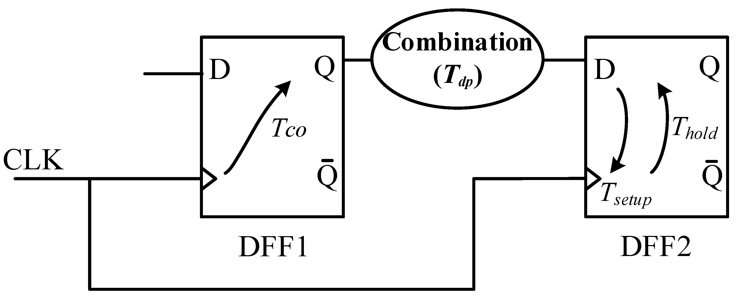
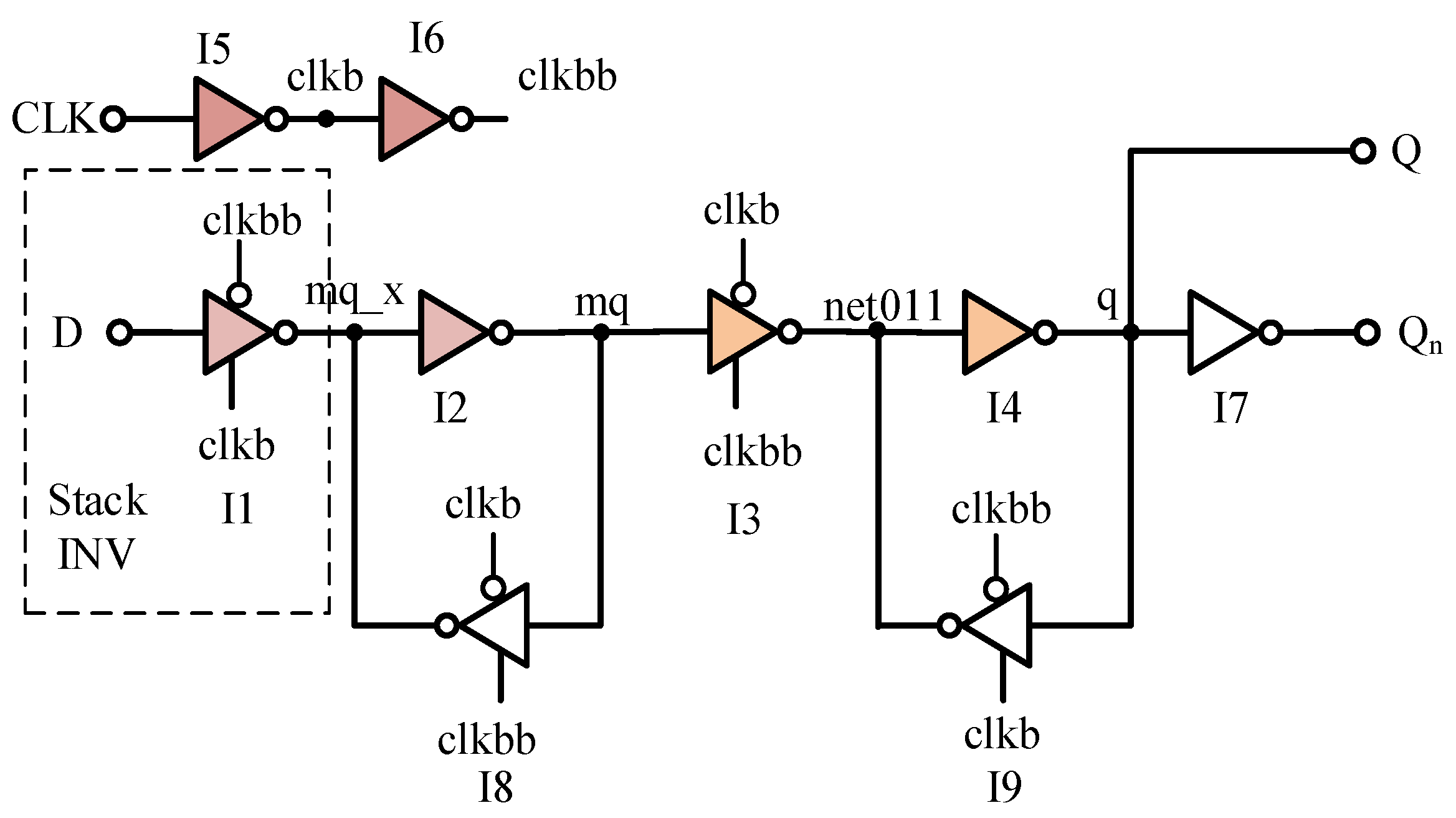
A master-slave flip-flop is the most commonly used flip-flop in circuits. As shown in Figure 1, in order to verify the reliability of the flip-flop, STA checks two types of timing constraints: setup time and hold time. After correctly capturing the logical value, there is a delay from the clock to the output, during which the captured value propagates to the flip-flop output, as shown in Figure 2.
The setup time is the minimum time that the input D must remain stable before the clock rising edge. For the master-slave flip-flop, the input must be propagated through I1 and I2 before the clock rising edge comes, so as to ensure that the voltage at both ends is equal when I8 is turned on; otherwise, the cross-coupled inverters I2 and I8 will stay at an incorrect value. Thus, the expression of setup time of the flip-flop is:
T s e t u p = T I 1 + T I 2
The hold time is the minimum time that the input D must remain stable after the clock rising edge. The hold time is actually to ensure the data on the D pin cannot affect the data sampled by the flip-flop after the clock rising edge. Thus, I1 must be closed when the rising edge of the clock is approaching. However, since the delay of D pin to I1 and CLK to I1 are different, the data at the D pin must remain unchanged until the CLK signal reaches I1. Therefore, the expression of hold time of the flip-flop is:
T h o l d = T I 5 + T I 6
The propagation delay Tcq is the delay from the start of the clock rising edge to the output Qn of the flip-flop. The expression of Tcq can be written as:
T c q = T I 5 + T I 6 + T I 3 + T I 4

3. Statistical Delay of Flip-Flop

The proposed flip-flop is composed of a stack structure and inverter. This section first introduces the analytical models of a stack structure and inverter. Then, the statistical delay model of the flip-flop in subthreshold region is modeled under the given distribution of process variation, and the expressions of cell step delay statistics are derived. Furthermore, delay variance and maximum and minimum delays are used to describe the effect of process variation on delay.

3.1. Delay Model for Inverter

In the subthreshold region, the leakage current of NMOS is expressed as (4), where λ is the drain-induced barrier lowering (DIBL) coefficient, m is the subthreshold slope factor, Vt is the thermal voltage, µn is the carrier mobility, Cox is the oxide capacitance for unit area, and Vthn is the threshold voltage of NMOS.
I s u b = I 0 W L e V g s V t h n m V t e λ V d s m V t 1 e V d s V t
Here,
I 0 = μ n C o x W L m 1 V t 2
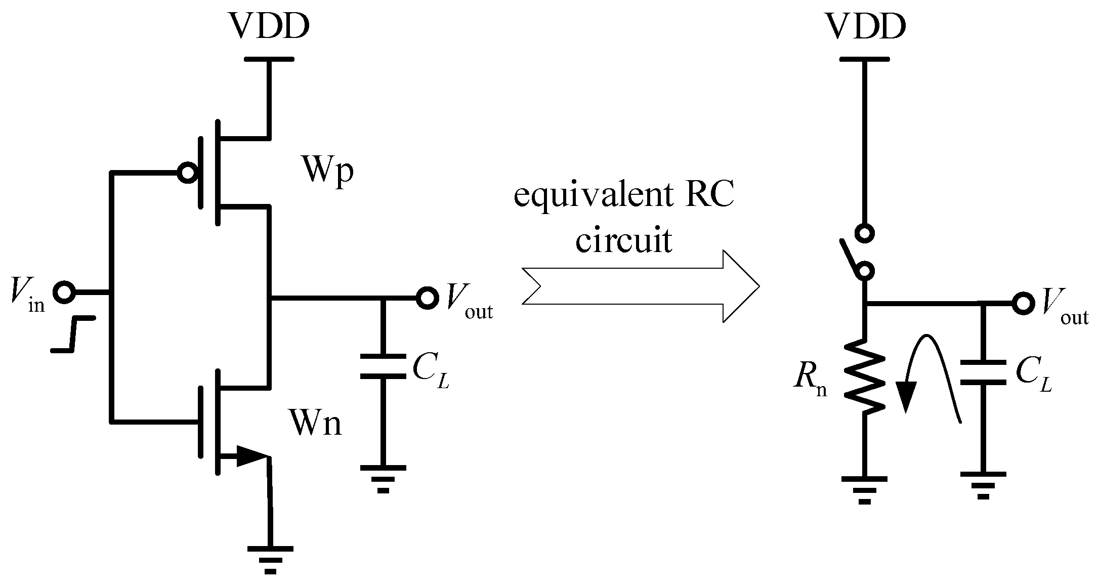
When the step input jumps from 0 to 1, the NMOS of the inverter is discharging, and the NMOS can be equivalent to a resistance R. The equivalent circuit is shown in Figure 3, and the current through R is shown as (4).
Cell propagation delay refers to the time difference between the output voltage reaching 50%Vdd and the input voltage reaching 50%Vdd, so the expression of the resistance R and propagation delay is as follows:
R = 1 V d d 2 V d d 2 V d d V I s u b d V
T s t e p = ln 2 R C L
Substituting Isub from (4) in (6), the expression of R and Tstep can be written as (8) and (9):
R = 2 m V t I 0 W L e V d d m V t λ 2 V d d 0.5 λ V d d + m V t e 0.5 λ V d d m V t λ V d d + m V e λ V d d m V t e V t h m V t
T s t e p = ln 2 2 m V t I 0 W L e V d d m V t λ 2 V d d . 0.5 λ V d d + m V t e 0.5 λ V d d m V t λ V d d + m V e λ V d d m V t e V t h m V t C L
The statistical variation of the threshold voltage (Vth) is a critical design consideration. It is a well-established practice to model Vth as a normal distribution [24]. Adopting this established model, Vth~N(µ, σ), we analyze the cell delay, which consequently follows the lognormal distribution shown in (10).
T s t e p ~ L N μ m V t + ln B , σ m V t
Here,
B = ln 2 2 m V t I 0 W L e V d d m V t λ 2 V d d 0.5 λ V d d + m V t e 0.5 λ V d d m V t λ V d d + m V t e λ V d d m V t C L
The maximum/ minimum delay can be computed by (12):
T d max / min = e μ T d ± 3 σ T d
where μTd and σTd refer to the expected value and standard deviation of inverter delay, respectively, shown as (13) and (14).
μ T d = μ m V t + ln B
σ T d = σ m V t

3.2. Delay Model for Gate with Stack Structure

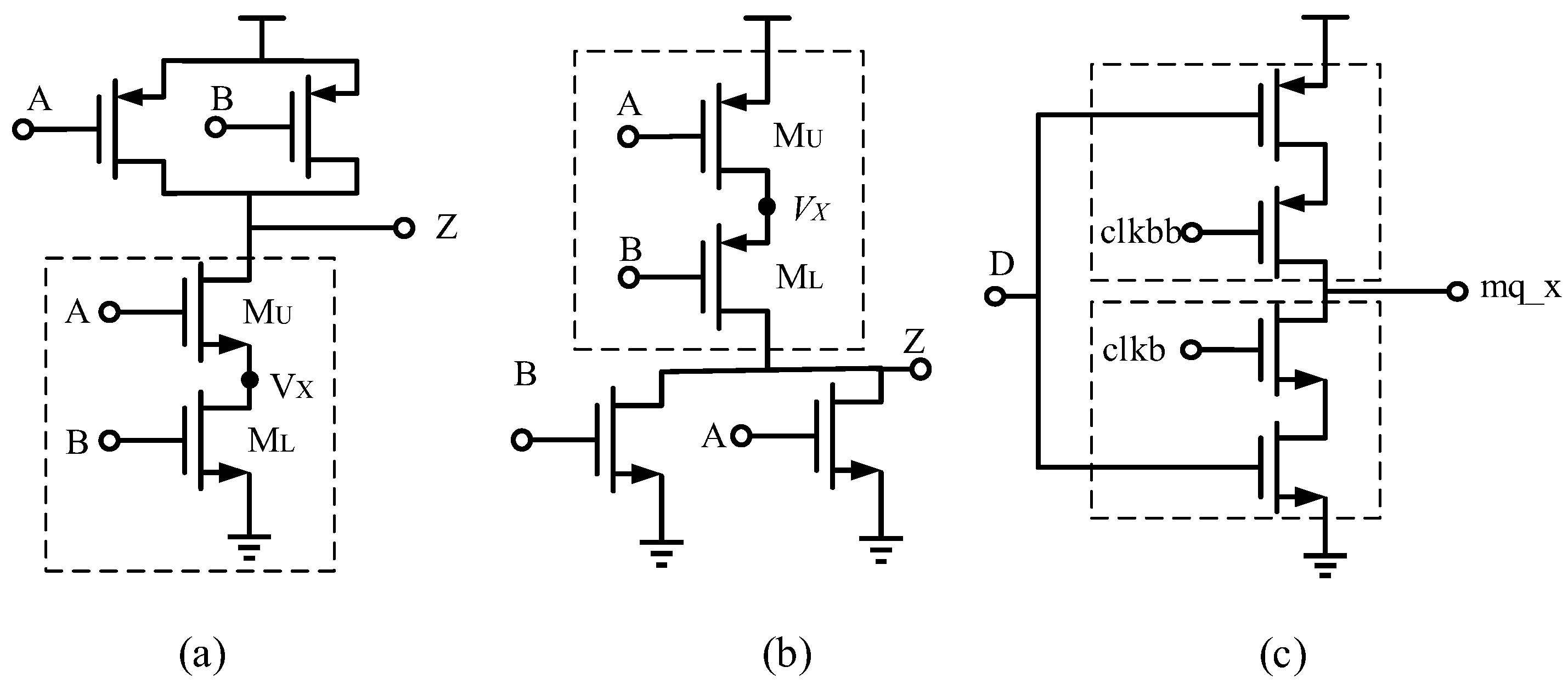
In a stacked structure, transistors are connected in series to charge and discharge with the same current. The most typical stack structure is a pull-down structure with a NAND gate and a pull-up structure with a NOR gate, as shown in Figure 4a,b. Figure 4c refers a stack inverter which is often used in the flip-flop. Thus, the statistical timing model of stack inverter can be derived by the NAND gate for rise transition and the NOR gate for fall transition. The leakage current of MU and ML of stacks for NMOS are shown as (15)–(17), where γ is the body effect coefficient, and VthU and VthL are the threshold voltages of MU and ML.
I M U = A W U e V g V X V t h U + γ V X λ V V X m V t 1 e V V X V t
I M L = A W L e V g V t h L + λ V X m V t 1 e V X V t
A = μ n C o x m 1 / L V t 2
Considering that IMU = IML, Vg = Vdd, 1 e V x V t 1 , and λVX ≈ 0, the following can be derived:
W U e V d d V X V t h U + γ V X λ V m V t = W L e V d d V t h L m V t 1 e V X V t
Finally, VX is derived:
V X = V t ln W L e V t h L V t h L m V t e λ V m V t + W L W L
Substituting VX in (15), the expression of R in stack structure can be written as:
R = 3 V d d 4 1 A W L e V d d m V t e V t h L m V t + 2 m V t A W U λ 2 V d d e V d d m V t 0.5 λ V d d + m V t e 0.5 λ V d d m V t λ V d d + m V e λ V d d m V t e V t h U m V t
Substituting R in (7), the propagation delay is shown as:
T s t e p = B 1 e V t h L m V t + B 2 e V t h U m V t
where
B 1 = ln 2 3 V d d 4 1 A W L e V d d m V t C L
B 2 = ln 2 2 m V t A W U λ 2 V d d e V d d m V t 0.5 λ V d d + m V t e 0.5 λ V d d m V t λ V d d + m V t e λ V d d m V t e V t h U m V t C L
Since the threshold voltage VthL and VthU approximately follows the normal distribution, which can be abbreviated as VthL~N(µ1, σ1), VthU~N(µ2, σ2), then
B 1 e V t h L m V t L N μ 1 m t + ln B 1 , σ 1 m V t
B 2 e V t h L m V t L N μ 2 m V t + ln B 2 , σ 2 m V t
According to the properties of lognormal distribution, the variance and mean of the cell delay can be obtained as:
D T s t e p = ln e 2 μ 1 + σ 1 2 e σ 1 2 1 + e 2 μ 2 + σ 2 2 e σ 2 2 1 e μ 1 + 0.5 σ 1 2 + e μ 1 + 0.5 σ 1 2 2 + 1
E T s t e p = ln e μ 1 + 0.5 σ 1 2 + e μ 1 + 0.5 σ 1 2 D T s t e p 2
It is worth noting that our model assumes the threshold voltages of the stacked transistors are independent. In reality, a weak spatial correlation may exist. Incorporating this correlation would add a covariance term to the variance calculation, significantly increasing model complexity. We adopt the independence assumption as a practical simplification, a common practice in analytical modeling to maintain tractability. The strong agreement between our results and Monte Carlo simulations, as shown below, suggests this simplification is reasonable for the structures under study.
The maximum and minimum delay values under different voltages for stacked gates including NAND, NOR, stacked inverters for rise/fall transitions can be obtained by (12), and the results are shown in Table 1, Table 2, Table 3 and Table 4, respectively. It can be found that the accuracy of the maximum (minimum) delay of model [22,25] degrades distinctly to 5.0X (4.2X) for the NAND gate, 7.8X (3.4X) for the NOR gate, 3X (2.6X) for the stacked inverter with rise transition, and 7.8X (4.1X) for the stacked inverter with fall transition. This demonstrates that it is much more advantageous to consider both transistor threshold variations than to consider only one transistor threshold voltage variation.

3.3. Delay Model for Flip-Flop

In this section, we derive the statistical delay model for a flip-flop, which consists of multiple logic stages. To provide a clear overview of the derivation process, the overall workflow is illustrated in Figure 5.
When the input voltage is a rising edge, the expression of the input signal Vin(t) is shown as follows, where T represents the rising transition time:
V i n ( t ) = V d d t T , 0 t T V d d , t > T
When the input transition time T is considered, the expression for the subthreshold current can be expressed as follows:
I s u b = I 0 W L e V d d t T V t h m V t , 0 < T < τ I 0 W L e V d d V t h m V t , t > T
According to the definition of delay and the capacitance charge and discharge formula, the following expression can be obtained:
V d d 2 C L = 0 T d + T 2 I d s d t
By substituting Equation (29) into Equation (30), (31) can be obtained. After solving the integral, the propagation delay Tdi is shown as (32).
V d d 2 C L = 0 T I 0 W L e V d d t T V t h m V t d t + T T d i + T 2 I 0 W L e V d d V t h m V t d t
T d i = V d d C L 2 I 0 W L e V t h V d d m V t + 1 2 e V d d m V t m V t V d d e V d d m V t 1 T
From the observation of (32), it can be seen that the first half of Tdi is independent of the transition time T and can be represented by Tdi0, and the second half is related to the transition time and can be represented by TdiT. Thus, Tdi can be written as the linear combination of Tdi0 and TdiT, which is shown as (33).
T d i = T d i 0 + T d i T
Here,
T d i 0 = V d d C L 2 I 0 W L e V t h V d d m V t T d i T = 1 2 e V d d m V t m V t V d d e V d d m V t 1 T
It can be obtained that Tdi is a linear combination of step delay T d i 0 and input transition time T, as shown in the following equation:
T d i = T d i 0 + β 1 T
Figure 5 shows the relationship between the input and output voltages of two adjacent gates with time. Vout,i−1 is the output of the previous gate and the input of current gate, Vout,i is the output of current gate, Ti−1 is the input transition time of previous gate, and Ti is the input transition time of current gate.
According to the capacitance charge and discharge formula and the definition of input transition time, following expression can be obtained.
V d d C L = 0 T i I 0 W L e V d d t T i 1 V d d V t h m V t e λ V d s m V t 1 e V d s V t d t
The step delay of the previous gate can be related to the propagation delay of the current gate.
T d i = T d i 0 + β i T d i 1 0
Here T d i 0 is the step delay of the current gate, T d i 1 0 is the step delay of the previous gate, and Tdi is the propagation delay of the previous gate. They can be obtained through one-time nominal SPICE simulation. Therefore, the scale factor βi can be derived directly by Equation (38).
β i = T d i T d i 0 T d i 1 0
The propagation delay for each stage is shown as follows:
T d 1 = T d 1 0 T d 2 = T d 2 0 + β 2 T d 1 0 ... T d i 1 = T d i 1 0 + β i 1 T d i 2 0 T d i = T d i 0 + β i T d i 1 0
Thus, the expression of path delay can be written as:
T p = T d 1 + T d 2 + ... + T d i 1 + T d i = T d i 0 + j = 2 j = i 1 + β i T d j 1 0
Since each step delay distribution is independent, the delay variance of the path can be obtained as:
D T p = D T d i 0 + j = 2 j = i 1 + β i 2 D T d j 1 0
According to the calculation methods of setup time, hold time, and propagation delay Tcq, as shown in Figure 6, the variance expression of setup time, hold time, and Tcq can be obtained as (42), (43), and (44).
D T s e t u p = D T d I 2 0 + 1 + β I 2 2 D T d I 1 0
D T h o l d = D T d I 6 0 + 1 + β I 6 2 D T d I 6 0
D T c q = D T d I 4 + 1 + β I 4 D T d I 3 + 1 + β I 6 D T d I 6 + 1 + β I 5 D T d I 5
Table 5, Table 6 and Table 7 present the error percent of the hold time, setup time, and propagation delay under different voltages. The inter-stage correlation is considered during the calculation of delay. The hold time is calculated in a similar way to that of [25]. For hold time, the error of standard deviation, maximum delay, and minimum delay are all within 7%. For setup time, the error of standard deviation, maximum delay, and minimum delay are all within 6%. For propagation delay, the error of standard deviation, maximum delay, and minimum delay are all within 5%. Compared with the threshold voltage variation of only one transistor considered in [22,25], the accuracy of the proposed method is much improved.

4. Statistical Delay Model of Sequential Path

The sequential path is composed of the combined logic path and flip-flop, as shown in Figure 7. In the previous section, we have modeled the statistical delay model of the flip-flop. In this section, we combine the statistical delay model of the flip-flop and the combination logic circuit to obtain the statistical delay model of the sequential path.

4.1. Relative Sensitivity of Step Delay

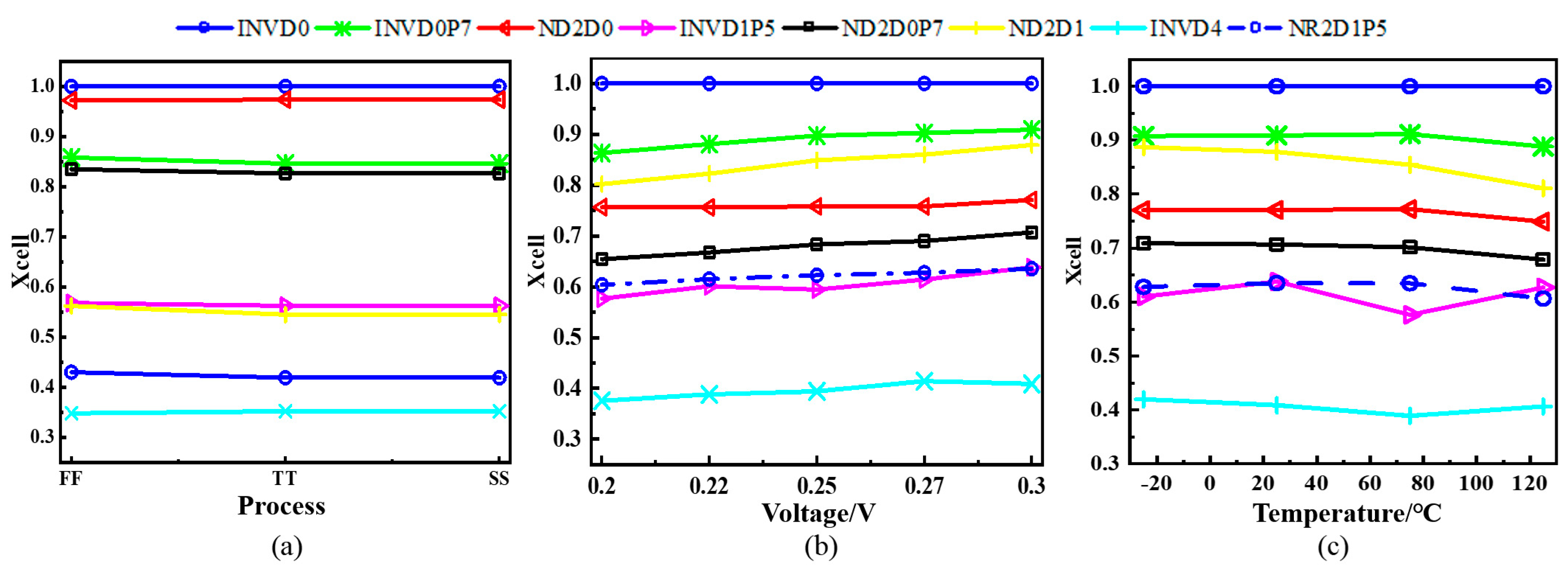
In this paper, the relative step delay relative sensitivity Xcell [15] is used to eliminate the influence of PVT on the computational complexity of step delay variance. Relative step delay sensitivity refers to the ratio of step delay sensitivity of different gates to that of reference gate which is inverter in this experiment, and its expression is shown in (45). The relationship between Xcell of each gate and PVT is shown in Figure 8. It can be seen from the simulation results that the Xcell basically remains unchanged under different PVT values.
X c e l l = D 1 / 2 / E T d c e l l 0 D 1 / 2 / E T d r e f 0

4.2. Gate Step Delay Variance

The gate step delay variance can be expressed as:
D T d i 0 = D T d i 0 E 2 T d i 0 E 2 T d i 0 = X c e l l , i 2 D T d r e f 0 E 2 T d r e f 0 T d i 0 2 e 0.5 D V t h i m V t
Xcell is independent of PVT, the lookup table of Xcell can be obtained only by MC simulation of each cell under a set of PVT conditions, and the nominal delay of the cell and the variance of the threshold voltage can be obtained in a short simulation time.

4.3. Sequential Path Delay Variation Model

According to [26], the expression of output voltage Vout in Figure 9 can be obtained.
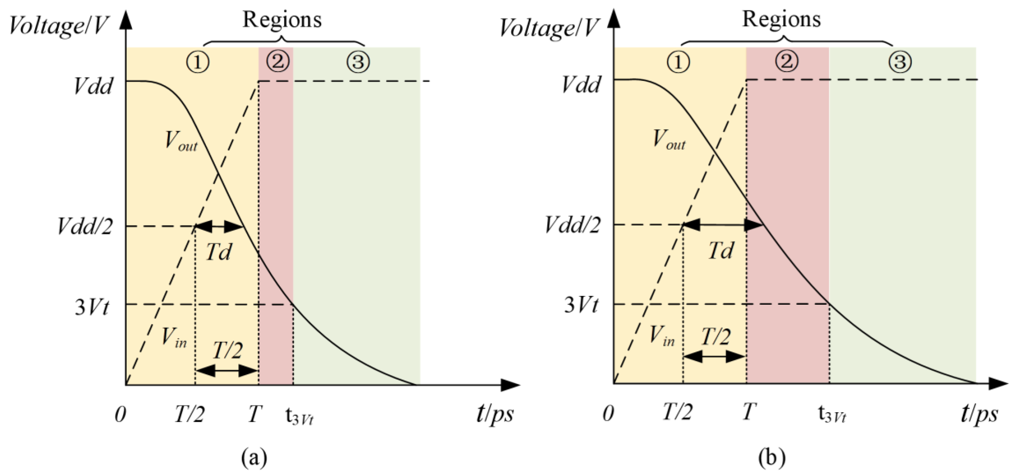
V o u t = m V t λ ln K λ T V d d C L e V d d m V t T t 1 + e λ V d d m V t , 0 < t < T m V t λ ln e λ V o u t , T m V t + K λ e V d d m V t m V t C L t T , T < t < t 3 V t V t ln 1 + e 3 1 e K e V d d / ( m V t ) V t C L t t 3 V t , t > t 3 V t
K = I 0 n W n L e V t h m V t
According to the definition of delay, that is, the time difference between the output voltage reaching 50%Vdd and the input voltage reaching 50%Vdd, as shown in (49), the calculation of delay is divided into two cases according to the case of input: (1) Under the condition of fast input, the time point of Vout = 0.5Vdd is located in region 1, as shown in Figure 8a. (2) Under the condition of slow input, the time point of Vout = 0.5Vdd is located in region 2, as shown in Figure 8b. By combining (47) and (49), the expression of delay under fast and slow inputs can be obtained, as shown in (50) and (51).
T d = t | V o u t = 0.5 V d d t | V i n = 0.5 V d d
T d f = C L m V t K λ e V d d m V t e λ V d d 2 m V t e λ V d d m V t + 1 2 m V t V d d T = T d 0 + 1 2 m V t V d d T
T d s = m V t V d d ln V d d C L K λ T e λ V d d 2 m V t e λ V d d m V t 1 2 T
The main sources of delay variation of the cell include (1) the variations of threshold voltage and (2) variations caused by input transition time T. These two variations come from different transistors. According to the independence principle of random variables, the delay variation of the cell can be obtained, as shown in Equation (52).
D T d t o t a l = D T d V t h + D T d s l e w
Thus, under the condition of fast input, there are two variances, which are caused by the threshold voltage variation and input transition time variation, represented as D(Tdf,vth) and D(Tdf,slew), respectively. This is also true under the slow input condition, and the variances are expressed as D(Tds,vth) and D(Tds,slew). The expressions are shown as (53)~(56).
D T d f , V t h = C L m V t I 0 W L λ e V d d m V t e λ V d d 2 m V t e λ V d d m V t D e V t h m V t
D T d s , V t h = T V d d 2 D V t h
D T d f , s l e w = 1 2 m V t V d d 2 D T
D T d s , s l e w = m V t V d d + T d s T 2 D T
According to the input slew of current gate and previous gate, the delay variation can be divided into “fast and slow”, “fast and fast”, “slow and fast”, and “slow and slow” for analysis. For the case that both current gate and previous gate are slow inputs, it is only possible to occur when two cells are very large driving cells to drive very small cells, which will not occur in the actual circuit, so we only analyze the first three cases.
(1)
Fast and slow:
D T d i = T i 1 V d d 2 D V t h i + ξ i 2 D T d i 1 0
ξ i = m V t V d d T i 1 T d i 1 0 + T d i T d i 1 0
D T p i = D T p i 1 + T i 1 V d d 2 D V t h i + ξ i 2 + 2 ξ i D T d i 1 0
(2)
Fast and fast:
D T d i = D T d i 0 + ξ i 2 D T d i 1 0
D T p i = D T p i 1 + D T d i 0 + ξ i 2 + 2 ξ i D T d i 1
(3)
Slow and fast:
D T d i = D T d i 0 + ξ i 2 D T d i 2 0
D T p i = D T p i 1 + D T d i 0 + 2 1 + ξ i 1 ξ i + ξ i 2 D T d i 2 0
Since the sequential logical path is composed of a flip-flop and a combination logical path, the statistical delay model of the sequential path can be obtained by combining the statistical timing model of the flip-flop and the combination logical path, as shown in (64).
D T p i , t o t a l = D T c q + D T p i
The path delay approximately follows a lognormal distribution, assuming that the distribution satisfies Tp~LN (µTp, σTp2), and the geometric mean of the lognormal distribution obtained by one-time SPICE simulation of the Tp is shown in the following equation:
T p n o m i n a l = e μ t p
Then, the expression of µTp is:
μ T p = ln T p n o m i n a l
According to the nature of lognormal distribution, its variance is calculated as:
D T p = e σ T p 2 1 e 2 μ T p + σ T p 2
To facilitate the solution of the distribution parameters µTp and σTp, coefficient K can be defined as:
K = D T p T p n o m i n a l 2 = e σ T p 2 1 e σ T p 2
It can be obtained by solving (67):
σ T p = ln 1 2 + K + 1 4
Substituting (66) and (69) into (70) gives the maximum and minimum delays of the timing path.
T p m a x / m i n = e u t p ± 3 σ t p

5. Experiments and Discussion

In order to verify the accuracy of the proposed statistical delay model, this section verifies the model proposed in the previous sections on the ISCAS’89 benchmark circuit, and the supply voltage given operates in the subthreshold region. The whole experiment takes the MC simulation results as the gold standard and compares them with other methods.

5.1. Experimental Setup

In this section, the proposed statistical timing model for sequential path was validated by using the process of TSMC28nm in the subthreshold region. The digital circuit flow is adopted to verify the proposed model by analyzing multiple benchmark circuits in ISCAS’89. The RTL of the benchmark circuit is converted into a gate level netlist by synthesis, and then the path netlist is extracted by Prime Time. The critical paths selected for validation from these benchmarks feature diverse logic depths, various cell types, and realistic fan-out conditions, ensuring a comprehensive test of our model’s performance on complex sequential paths. First, the timing modeling of the inverter and stack structure is carried out, and the propagation delay statistical value of the flip-flop are obtained by using the inter-correlation between stages. Then, the lookup table of the relative delay sensitivity Xcell0 of the combinational logical cell is obtained by analytical method, and the statistical delay of the combination logic path are further obtained by inter-stage correlation. Finally, the statistical delay model of the sequential path is obtained by combining the previous two steps.

5.2. Experimental Result and Analysis

In this section, the model proposed in this paper is verified and analyzed through three variation values: path delay standard deviation and path maximum and minimum delays.
As shown in Table 8, Table 9 and Table 10, the statistical delay value of one path is verified under different processes, voltages, and temperatures. Under the process corners FF, TT, and SS, the mean error of the standard deviation of the path is 4%, the mean error of the maximum delay value is 5.3%, and the mean error of the minimum delay value is 7.5%. Under 0.3 V, 0.27 V, and 0.25 V supply voltages, the mean error of standard deviation is 3.4%, the mean error of maximum delay value is 4.7%, and the mean error of minimum delay value is 8.8%. At −25 °C, 25 °C, and 75 °C, the mean error of standard deviation is 1.4%, the mean error of maximum delay is 5.2%, and the mean error of minimum delay is 8.1%.
In addition to process and voltage variations, the model’s performance was also evaluated across a range of operating temperatures. As presented in Table 11, the model maintains high accuracy at -25 °C, 25 °C, and 75 °C, with an average error of only 1.4% for standard deviation, demonstrating its thermal robustness.
In order to further verify the accuracy of the model, five circuits are selected from ISCAS’89 benchmark, namely s27, s1196, s13207, s15850, and s1423. Among them, s1423 has the largest number of cells, which is 56. The comparison error results of three metrics with respect to 10,000 runs of MC simulation are listed in Table 12.
The percentage error for each metric is calculated using the following formulas, where Predicted refers to the value from our model, and MC refers to the value from Monte Carlo simulation:
E r r o r s t d = σ P r e d i c t e d σ M C / σ M C × 100 %
E r r o r m a x = D e l a y m a x _ P r e d i c t e d D e l a y m a x _ M C / D e l a y m a x _ M C × 100 %
E r r o r m i n = D e l a y m i n _ P r e d i c t e d D e l a y m i n _ M C / D e l a y m i n _ M C × 100 %
From the table, the average errors are 5.23%, 5.62%, and 5.92% for standard deviation, maximum delay, and minimum delay, respectively. Compared with other two methods, it can be found that the standard deviation, maximum delay, and minimum delay prediction achieve up to 6.0X (10.2X), 4.3X (4.2X), and 2.7X (2.8X) precision improvements, respectively. This indicates that our proposed model is much more accurate than the method in [15], which does not consider the inter-stage correlation, and the method in [18], which does not consider the influence of the clock path on the propagation delay Tcq.
Beyond its high accuracy, our model’s primary advantage is its computational efficiency. This efficiency arises from a fundamental methodological difference with Monte Carlo simulations. MC analysis is computationally expensive, as it relies on thousands of repetitive circuit simulations to achieve statistical convergence.
In contrast, our analytical model requires only a single nominal SPICE simulation to extract key parameters. The statistical moments are then computed directly via analytical expressions, a step with negligible computational cost. Essentially, our method replaces thousands of transient simulations with one nominal simulation and a simple calculation.
This approach provides a highly favorable time–accuracy trade-off. By maintaining high fidelity to the MC results while drastically reducing runtime, our model enables the rapid, iterative timing analysis essential for modern design cycles, a task where MC simulation is prohibitively slow.
The practical impact of this efficiency in industrial scenarios is significant. By providing fast and accurate statistical timing feedback, our model can be integrated into standard CAD flows to enable early, variation-aware design optimization. This can help reduce the number of costly design iterations and shorten the overall time to market. Furthermore, its high speed makes it a candidate for reducing the reliance on lengthy MC simulations during the final timing sign-off, potentially saving days of computation on large designs.

6. Conclusions

This paper presented an analytical statistical model for sequential path delay variation in low-voltage circuits, based on the lognormal distribution. We introduced a novel method to characterize the delay of complex structures, including stacked transistors and flip-flops, by decomposing the impact of multi-threshold voltage variations and resolving inter-stage correlations through a linear delay model. The use of relative delay sensitivity further enhances the model’s efficiency, allowing for rapid characterization across multiple PVT corners from a single nominal simulation.
Compared to purely mathematical or machine learning-based approaches, our analytical model offers distinct advantages in terms of interpretability and design insight. While ML models may achieve high accuracy after extensive training, our physics-based model provides a clear, transparent relationship between process parameters and timing variations without requiring a large dataset. This makes it particularly valuable for early-stage design exploration and optimization. A qualitative comparison summarizing these trade-offs against other state-of-the-art methods is provided in Table 13.
While the proposed framework demonstrates high accuracy and efficiency, several avenues for future research are identified to further enhance its robustness and applicability. The model’s scalability to advanced nodes like FinFETs is a promising direction; although this would require adapting the underlying device equations, the core methodology of linear decomposition and variance propagation remains applicable. The framework could also be extended to incorporate time-dependent aging effects, such as NBTI and HCI, by modeling their impact as a long-term shift in the threshold voltage distribution. Furthermore, a comprehensive evaluation using additional industrial metrics, such as Mean Absolute Error (MAE) and 95th-percentile delay, would further validate its practical utility for timing sign-off. Finally, while the model shows excellent agreement with extensive SPICE simulations, validation against silicon measurements from a test chip is the ultimate goal to confirm its real-world performance. Addressing these aspects will be the focus of our future investigations.
Author Contributions

Conceptualization, R.L., D.Z. and J.G.; methodology, R.L.; software, D.Z.; validation, R.L., D.Z. and J.G.; formal analysis, R.L.; investigation, R.L., D.Z. and J.G.; resources, J.G.; data curation, D.Z.; writing—original draft preparation, R.L. and D.Z.; writing—review and editing, R.L., D.Z. and J.G.; visualization, R.L. and D.Z.; funding acquisition, J.G. All authors have read and agreed to the published version of the manuscript.

Funding

This work was supported by the National Natural Science Foundation of China (Grant No. 62501305) and the Natural Science Foundation of Jiangsu Province under Grant BK20240637.

Institutional Review Board Statement

Not applicable.

Informed Consent Statement

Not applicable.

Data Availability Statement

The original contributions presented in the study are included in the article, further inquiries can be directed to the corresponding author.

Conflicts of Interest

The authors declare no conflicts of interest.

References

  1. Zhai, B.; Hanson, S.; Blaauw, D.; Sylvester, D. Analysis and mitigation of sensitivity in subthreshold design. In Proceedings of the International Symposium on Low Power Electronics and Design, San Diego, CA, USA, 8–10 August 2005; pp. 20–25. [Google Scholar]
  2. Mahmoudi, H.; Zimmermann, H. A new sampling technique for Monte Carlo-based statistical circuit analysis. In Proceedings of the Design, Automation & Test in Europe Conference & Exhibition, Lausanne, Switzerland, 27–31 March 2017; pp. 1277–1280. [Google Scholar]
  3. Singhee, A.; Rutenbar, R.A. Why Quasi-Monte Carlo is better than Monte Carlo or latin hypercube sampling for statistical circuit analysis. IEEE Trans. Comput.—Aided Des. Integr. Circuits Syst. 2010, 29, 1763–1776. [Google Scholar] [CrossRef]
  4. Singhee, A.; Rutenbar, R.A. From finance to flip flops: A study of fast Quasi-Monte Carlo methods from computational finance applied to statistical circuit analysis. In Proceedings of the International Symposium on Quality Electronic Design, San Jose, CA, USA, 26–28 March 2007; pp. 685–692. [Google Scholar]
  5. Collings, B.; Niederreiter, H. Random number generation and Quasi-Monte Carlo methods. J. Am. Stat. Assoc. 1993, 88, 699. [Google Scholar] [CrossRef]
  6. Zhang, L.; Chen, W.; Hu, Y.; Yu, B.; Zhou, Q. Correlation-preserved non-Gaussian statistical timing analysis with quadratic timing model. In Proceedings of the 42nd Design Automation Conference, Anaheim, CA, USA, 13–17 June 2005; pp. 83–88. [Google Scholar]
  7. Zhan, Y.; Strojwas, A.J.; Li, X.; Pileggi, L.T.; Newmark, D.; Sharma, M. Correlation-aware statistical timing analysis with non-Gaussian delay distributions. In Proceedings of the 42nd Design Automation Conference, Anaheim, CA, USA, 13–17 June 2005; pp. 77–82. [Google Scholar]
  8. Ramprasath, S.; Vijaykumar, M.; Vasudevan, V. A skew-normal canonical model for statistical static timing analysis. IEEE Trans. Very Large Scale Integr. (VLSI) Syst. 2016, 24, 2359–2372. [Google Scholar] [CrossRef]
  9. Cheng, L.; Xiong, J.; He, L. Non-Gaussian statistical timing analysis using second-order polynomial fitting. IEEE Trans. Comput.—Aided Des. Integr. Circuits Syst. 2009, 28, 130–133. [Google Scholar] [CrossRef]
  10. Vijaykumar, M.; Vasudevan, V. Statistical static timing analysis using a skew-normal canonical delay model. In Proceedings of the Design, Automation & Test in Europe Conference & Exhibition, Dresden, Germany, 24–28 March 2014; pp. 1–6. [Google Scholar]
  11. Yan, H.; Shi, X.; Xuan, C.; Cao, P.; Shi, L. An adaptive delay model for timing yield estimation under wide-voltage range. In Proceedings of the 26th Asia and South Pacific Design Automation Conference, Tokyo, Japan, 18–21 January 2021; pp. 272–277. [Google Scholar]
  12. Deng, F.; Feng, Y.; Niu, D.; Wu, X.; Jin, Z. SD-SSTA: Statistical Static Time Analysis Algorithm Considering Skewed Distribution. In Proceedings of the 2024 2nd International Symposium of Electronics Design Automation, Xi’an, China, 10–13 May 2024; pp. 518–523. [Google Scholar]
  13. Shiomi, J.; Ishihara, T.; Onodera, H. Statistical timing modeling based on a lognormal distribution model for near-threshold circuit optimization. IEICE Trans. Fundam. Electron. Commun. Comput. Sci. 2015, E98.A, 257–266. [Google Scholar] [CrossRef]
  14. Shiomi, J.; Ishihara, T.; Onodera, H. Microarchitectural-level statistical timing models for near-threshold circuit design. In Proceedings of the 20th Asia and South Pacific Design Automation Conference, Chiba, Japan, 19–22 January 2015; pp. 87–93. [Google Scholar]
  15. Alioto, M.; Scotti, G.; Trifiletti, A. A novel framework to estimate the path delay variability on the back of an envelope via the fan-out-of-4 metric. IEEE Trans. Circuits Syst. I Regul. Pap. 2017, 64, 2073–2085. [Google Scholar] [CrossRef]
  16. Cui, Y.; Shan, W.; Dai, W.; Liu, X.; Guo, J.; Cao, P. An improved path delay variability model via multi-level fan-out-of-4 metric for wide-voltage-range digital CMOS circuits. Chin. J. Electron. 2023, 32, 375–384. [Google Scholar] [CrossRef]
  17. Cao, P.; Liu, Z.; Wu, J.; Guo, J.; Yang, J.; Shi, L. A statistical timing model for low voltage design considering process variation. In Proceedings of the IEEE/ACM International Conference on Computer-Aided Design, Westminster, CO, USA, 4–7 November 2019; pp. 1–8. [Google Scholar]
  18. Fisher, S.; Dagan, R.; Blonder, S.; Fisher, A. An improved model for delay/energy estimation in near-threshold flip-flops. In Proceedings of the IEEE International Symposium of Circuits and Systems, Rio de Janeiro, Brazil, 15–18 May 2011; pp. 1065–1068. [Google Scholar]
  19. Cao, P.; Liu, Z.; Guo, J.; Pang, H.; Wu, J.; Yang, J. Accurate and efficient interdependent timing model for flip-flop in wide voltage region. In Proceedings of the IEEE International New Circuits and Systems Conference, Munich, Germany, 24–26 June 2019; pp. 1–4. [Google Scholar]
  20. Balef, H.A.; Jiao, H.; de Gyvez, J.P.; Goossens, K. An analytical model for interdependent setup/hold-time characterization of flip-flops. In Proceedings of the International Symposium on Quality Electronic Design, Santa Clara, CA, USA, 14–15 March 2017; pp. 209–214. [Google Scholar]
  21. Agarwal, M.; Saurabh, S. An efficient timing model of flip-flops based on artificial neural network. In Proceedings of the 2021 ACM/IEEE 3rd Workshop on Machine Learning for CAD, Virtual Event, 16–20 August 2021; pp. 1–6. [Google Scholar]
  22. Kahng, A.B.; Lee, H. Timing margin recovery with flexible flip-flop timing model. In Proceedings of the International Symposium on Quality Electronic Design, Santa Clara, CA, USA, 3–5 March 2014; pp. 496–503. [Google Scholar]
  23. Chen, Y.; Tian, L.; Ye, Y.; Shi, C.; Yan, H. A Statistical Static Timing Analysis Algorithm Based On Graph Neural Network. In Proceedings of the 2025 International Symposium of Electronics Design Automation, Hong Kong, China, 9–12 May 2025; pp. 262–267. [Google Scholar]
  24. Oruganti, A.; Ranganathan, N. Leakage power reduction in dual-Vdd and dual-Vth designs through probabilistic analysis of Vth variation. In Proceedings of the 19th International Conference on VLSI Design Held Jointly with 5th International Conference on Embedded Systems Design, Hyderabad, India, 3–7 January 2006; pp. 65–70. [Google Scholar]
  25. Cao, P.; Xu, W.; Wu, Y.; Liu, W.; Wang, Y. Subthreshold delay variation model considering transitional region for input slew. Electronics 2023, 12, 615. [Google Scholar] [CrossRef]
  26. Corsonello, P.; Frustaci, F.; Lanuzza, M.; Perri, S. Over/Undershooting effects in accurate buffer delay model for sub-threshold domain. IEEE Trans. Circuits Syst. I Regul. Pap. 2014, 61, 1456–1464. [Google Scholar] [CrossRef]
Figure 1. Master-slave flip-flop structure.
Applsci 15 12560 g001
Figure 2. Definition of setup time, hold time, and propagation delay.
Applsci 15 12560 g002
Figure 3. Equivalent circuit during the inverter switching.
Applsci 15 12560 g003
Figure 4. Stack structures including (a) NAND; (b) NOR; and (c) stack INV.
Applsci 15 12560 g004
Figure 5. The key steps of our flip-flop delay model derivation.
Applsci 15 12560 g005
Figure 6. The relationship between the input and output voltages of two adjacent gates with time.
Applsci 15 12560 g006
Figure 7. Structure of sequential path.
Applsci 15 12560 g007
Figure 8. Relation between relative step delay relative variability Xcell and PVT. (a) Process; (b) voltage; (c) temperature.
Applsci 15 12560 g008
Figure 9. Example of slow/fast input slew. (a) Fast input slew; (b) slow input slew.
Applsci 15 12560 g009
Table 1. Maximum and minimum delays of NAND gate.
Maximum DelayMinimum Delay
Voltage (V)[22,25]This Work[22,25]This Work
0.326.2%5.4%29.8%8.9%
0.2719.8%0.1%21.7%1.6%
0.2512.7%6.2%18.1%6.2%
Average19.5%3.9%23.2%5.5%
Improvement 5.0X1.0X4.2X1.0X
Table 2. Maximum and minimum delays of NOR gate.
Maximum DelayMinimum Delay
Voltage (V)[22,25]This Work[22,25]This Work
0.316.6%0.9%31.8%8.3%
0.2715.4%1.00%23.2%3.5%
0.2512.8%3.8%18.7%9.7%
Average14.9%1.9%24.5%7.1%
Improvement 7.8X1.0X3.4X1.0X
Table 3. Maximum and minimum delays of stack inverter for rise transition.
Maximum DelayMinimum Delay
Voltage (V)[22,25]This Work[22,25]This Work
0.341.6%5.8%20.1%8.0%
0.2734.8%0.3%10.0%3.5%
0.2526.2%6.4%9.8%3.9%
Average34.2%4.1%13.3%5.1%
Improvement 8.3X1.0X2.6X1.0X
Table 4. Maximum and minimum delays of stack inverter for fall transition.
Maximum DelayMinimum Delay
Voltage (V)[22,25]This Work[22,25]This Work
0.313.9%1.5%31.7%8.1%
0.2715.6%0.8%24.6%1.6%
0.2512.7%3.3%19.5%8.6%
Average14.1%1.8%25.3%6.1%
Improvement 7.8X1.0X4.1X1.0X
Table 5. Error in standard deviation and maximum and minimum delays with respect to 10k runs of MC simulation of hold time under different voltages.
Voltage (V)Standard DeviationMaximum DelayMinimum Delay
0.36.9%6.8%6.8%
0.274.1%5.9%6.3%
0.258.3%3.5%2.0%
Average6.4%5.4%5.0%
Table 6. Error in standard deviation and maximum and minimum delays with respect to 10k runs of MC simulation of setup time under different voltages.
Standard DeviationMaximum DelayMinimum Delay
Voltage (V)[22,25]This Work[22,25]This Work[22,25]This Work
0.355.0%1.0%27.0%1.9%24.6%2.3%
0.2741.8%2.6%22.8%0.3%22.2%4.7%
0.2528.2%5.5%15.5%4.4%17.0%0.2%
Average41.6%3.0%21.8%2.2%21.2%7.2%
Table 7. Error in standard deviation and maximum and minimum delays with respect to 10k runs of MC simulation of propagation delay under different voltages.
Standard DeviationMaximum DelayMinimum Delay
Voltage (V)[22,25]This Work[22,25]This Work[22,25]This Work
0.344.0%4.1%13.5%2.2%14.1%0.3%
0.2738.3%5.9%12.2%2.1%13.3%0.5%
0.2520.9%2.3%5.0%5.5%7.0%3.3%
Average34.4%4.1%10.2%3.3%11.5%1.3%
Table 8. Details of ISCAS’89 benchmark circuits and selected paths.
CircuitGate CountFlip-Flop CountPath Length
s271035
s11965291820
s13207795163816
s15850977253423
s14236577456
Table 9. Standard deviation and maximum and minimum delay errors of time sequence path delay under different processes.
ProcessStandard DeviationMaximum DelayMinimum Delay
FF4.7%7.7%6.9%
TT1.7%4.8%7.7%
SS5.6%3.5%7.9%
Average4%5.3%7.5%
Table 10. Standard deviation and maximum and minimum delay errors of time sequence path delay under different voltages.
Voltage (V)Standard DeviationMaximum DelayMinimum Delay
0.31.7%4.8%7.7%
0.272.9%5.0%8.6%
0.255.7%4.5%10.2%
Average3.4%4.7%8.8%
Table 11. Standard deviation and maximum and minimum delay errors of time sequence path delay under different temperatures.
Temperature (°C)Standard DeviationMaximum DelayMinimum Delay
−25 °C1.6%6.7%12.3%
25 °C1.7%4.8%7.7%
75 °C1.1%4.1%4.3%
Average1.4%5.2%8.1%
Table 12. Error in standard deviation and maximum/minimum delays with respect to 10k runs of MC simulation for the practical paths of iscas’89 benchmark in 0.3 V supply voltage and 25 °C TT corner.
CircuitStageStandard DeviationMaximum DelayMinimum Delay
[15][18]This Work[15][18]This Work[15][18]This Work
s27542.46%46.78%2.10%35.11%34.27%4.52%29.97%31.65%9%
s11962043.64%43.64%5.42%22.38%22.38%5.84%15.29%15.29%4.83%
s132071626.93%49.63%7.08%24.12%24.06%6.36%16.46%16.55%5.34%
s158502339.53%74.76%7.72%15.96%15.95%5.67%6.61%6.62%4.95%
s1423564.97%52.55%3.83%22.21%22.09%5.74%14.09%14.26%5.48%
Average--31.51%53.47%5.23%23.96%23.75%5.62%16.48%16.87%5.92%
Improvement (X)--6.0X10.2X1.0X4.3X4.2X1.0X2.7X2.8X1.0X
Table 13. Qualitative comparison of different SSTA methods.
FeatureMonte CarloFisher’s Model [18]ML-Based ModelThis Work
AccuracyGold StandardModerateHighHigh
SpeedVery LowHighHighVery High
InterpretabilityLowHighVery LowHigh
DataNoneNoneVery HighNone
FocusGeneralSequential CellsGeneralSequential Paths
Disclaimer/Publisher’s Note: The statements, opinions and data contained in all publications are solely those of the individual author(s) and contributor(s) and not of MDPI and/or the editor(s). MDPI and/or the editor(s) disclaim responsibility for any injury to people or property resulting from any ideas, methods, instructions or products referred to in the content.