Article

Low-Temperature RF Magnetron Sputtering of TiW Thin Films: Effects of the Bulk Plasma Characteristics on Film Growth

Department of Semiconductor Engineering, Gyeongsang National University, Jinju 52828, Republic of Korea
*
Author to whom correspondence should be addressed.
Appl. Sci. 2025, 15(22), 12300; https://doi.org/10.3390/app152212300
Submission received: 23 October 2025 / Revised: 12 November 2025 / Accepted: 18 November 2025 / Published: 19 November 2025
(This article belongs to the Special Issue Plasma Applications in Material Processing)

Abstract

TiW thin films with superior surface properties were deposited at room temperature using RF magnetron sputtering under low-temperature process conditions. The correlation between bulk plasma characteristics and thin-film properties was investigated as a function of applied RF power (200–600 W) and process pressure (1–10 mTorr). Plasma potential and ion density were measured using a Langmuir probe, while deposition rate, surface roughness, sheet resistance, and crystallinity were evaluated. Increasing the applied RF power simultaneously increased plasma potential and ion density, enhancing ion bombardment energy at both the target and substrate, which improved sputtering efficiency and deposition rate. Under low-temperature deposition, thermal stress induced by differences in thermal expansion between the film and substrate was minimal. However, limited surface diffusion of adatoms caused incomplete coalescence of nucleation islands, adversely affecting film crystallinity. Refractory metals such as tungsten exhibit strong dependence of residual stress and microstructure on deposition conditions, highlighting the importance of plasma and process parameters on TiW film properties. When RF power was increased, the enhancement in deposition rate outweighed the effect of increased ion energy, leading to tensile stress from void formation dominating over compressive stress induced by high-energy ions. This also contributed to increased grain size and reduced sheet resistance. In contrast, variations in process pressure had minor effects on plasma characteristics, resulting in limited changes in the deposited film properties.

1. Introduction

With the rapid advances of semiconductor device miniaturization and high integration, the significance of physical stacking-based three-dimensional (3D) integration technology at the wafer level has increasingly come to the forefront [1,2,3,4,5,6,7,8]. In particular, for memory device fabrication processes that require high-speed data transmission, 3D integration technology using through-silicon vias (TSVs) offers technological advantages by enhancing the integration density through vertical interconnections, reducing wiring delays, and significantly improving system bandwidth. The TSV formation process involves high-aspect-ratio silicon etching, the formation of a sidewall insulation layer, and copper plating [9]. Among these, depositing a barrier and seed layer before plating is essential for preventing metal diffusion and enhancing plating adhesion. TiW-based thin films, commonly used in this step, play a critical role in ensuring electrode reliability [10].
Recently, the development of high-performance semiconductor packaging technologies has placed increasingly stringent restrictions on the process temperatures. Conventional packaging processes have typically progressed sequentially through front-end-of-line (FEOL) (~1000 °C), back-end-of-line (BEOL) (~400 °C), and packaging (~250 °C) stages, assuming a gradual decrease in temperature [11]. In advanced packaging technologies, however, the boundary between BEOL and packaging processes has become ambiguous, and metal wiring processes may sometimes precede BEOL [12]. Accordingly, there is a growing demand for metal thin film deposition processes that can achieve excellent electrical properties and low surface roughness under low-temperature conditions below 200 °C. In particular, the development of deposition technologies that ensure stable barrier and seed layer formation at low temperatures has become imperative [13].
When chemical vapor deposition (CVD) processes are used to achieve uniform seed/barrier layer formation, excellent step coverage can be attained. Nevertheless, the high processing temperatures involved may cause thermal deformation of the device structures, which can adversely affect electrode reliability [14,15]. In particular, with the application of low-k or porous dielectrics as inter-metal dielectric (IMD) materials to reduce RC delay in metal wiring, the importance of low-temperature processing to ensure stability at the metal-dielectric interface is further emphasized [16]. Against this backdrop, the implementation of low-temperature deposition techniques for forming barrier and seed layers has become a critical task in BEOL and TSV processes. Consequently, there is an increasing demand for low-temperature physical vapor deposition (PVD) processes based on RF sputtering that can stably form metal thin films at temperatures below 200 °C [17].
Sputtering is a PVD-based thin-film deposition technique in which ions generated in plasma collide with a metal target to eject atomic-scale particles, which then deposit onto the substrate surface [18]. The thin film forms as atoms emitted from the target reach the substrate surface, undergo physical adsorption (physisorption) via van der Waals forces, and subsequently migrate across the surface through energy-driven surface diffusion [18]. In the initial stages of film formation, the energy of incident atoms and their surface mobility govern nucleation and growth mechanisms, which directly influence the crystallinity and morphology of the resulting film [19].
In high-temperature sputtering processes (typically above 300 °C), surface atom diffusion and rearrangement can be actively controlled by the substrate temperature. Under low-temperature sputtering conditions (<200 °C), however, thermal mobility is significantly limited, necessitating an additional energy source to facilitate atomic diffusion [17]. In this context, ion bombardment directed toward the substrate plays a crucial role by delivering kinetic energy directly to the surface [17,20]. This energy input enables surface atoms to overcome the diffusion barriers, promoting effective surface migration and atomic rearrangement. Furthermore, ion bombardment enhances surface diffusion, contributing to the removal of surface contaminants and weakly bonded atoms, improving the density and uniformity of the film. It can also induce localized recrystallization, improving film crystallinity and surface properties.
In TiW sputtering processes, refractory metals such as tungsten exhibit a strong dependence of residual stress and microstructure on deposition conditions, including temperature, pressure, and RF power [21]. In particular, under low-temperature processes, including room temperature deposition, materials such as titanium experience relatively small thermal stress variations upon cooling from the deposition temperature to ambient temperature, due to the minimal difference in thermal expansion coefficients between the film and the substrate [22,23]. This provides the advantage of relatively stable stress characteristics in the resulting film. However, at these low substrate temperatures, adatoms lack sufficient energy for surface diffusion, leading to the growth of small nucleation islands on the substrate. The coalescence of these islands is often incomplete, which in turn adversely affects the crystallinity of the deposited thin film. Under these conditions, the effects of process parameters and plasma characteristics serve as key factors that significantly influence the properties and crystallographic evolution of the thin film.
Radio-frequency (RF) sputtering is particularly advantageous for low-temperature film growth owing to its ability to induce strong ion bombardment at the substrate surface, even under reduced thermal conditions, outperforming conventional direct-current (DC) sputtering in this regard [17,24,25,26]. In an RF sputtering system, although a relatively low DC bias is applied to the target by a high-frequency power source, the bulk plasma achieves a high ionization efficiency through α-mode discharge, resulting in the generation of a dense ion population. Specifically, a strong electric field is established near the substrate because of the potential difference between the bulk plasma and the sheath region [27]. This facilitates active ion influx toward the substrate, enhancing energy transfer at the surface. As a result, surface atom mobility is increased, while loosely bound atoms are desorbed, leading to improvements in film crystallinity, density, surface roughness, and electrical properties.
Therefore, in low-temperature sputtering processes, a precise understanding of thin-film growth mechanisms based on the analysis of plasma characteristics and ion behavior is essential for ensuring high-quality film formation. This study examined the properties of the seed and barrier layers composed of TiW metals formed by RF magnetron sputtering under low-temperature conditions near room temperature. Thin films were deposited by varying key process parameters, including applied power and gas pressure. The resulting films were characterized in terms of thickness, surface roughness, resistivity, and crystallinity. Furthermore, plasma diagnostics using a Langmuir probe were conducted to analyze the correlation between the ion behavior in the bulk plasma and the resulting thin-film properties.

2. Experimental Setup and Method

An RF magnetron sputtering system (TERRA-T, ULTECH, Daegu, South Korea) was configured to investigate the sputtering process characteristics and plasma diagnostics of TiW thin films at low temperatures, as shown in Figure 1. The system consisted of three sputtering guns symmetrically arranged along an equal radial distance from the chamber center. Only Gun #1 was used in this study to ensure process reproducibility, with 13.56 MHz continuous-wave (CW) RF power applied. An RF generator and matching network were used to sustain the plasma discharge, and a vacuum pump and vacuum gauge were integrated to maintain a high-vacuum environment. A Langmuir probe diagnostic system was also installed for plasma characterization in the bulk region.
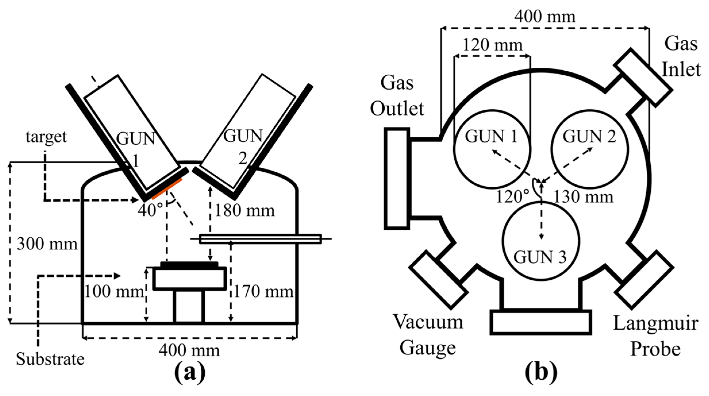
Figure 2 outlines the physical configuration of the process chamber. Figure 2a presents the front view of the chamber, which is cylindrical with a diameter of 400 mm, a height of 300 mm, and a total volume of approximately 0.033 m3. The height of the wafer chuck was fixed at 100 mm, and the distance between the chuck and sputtering gun was set to 180 mm. Figure 2b shows the top view, where each sputtering gun has a diameter of 120 mm. A water-cooling system was applied to maintain the target temperature. The three sputtering guns were symmetrically arranged 130 mm from the center of the chamber. A magnetron-type sputtering structure was adopted to ensure sufficient plasma density under low-pressure conditions (<10 mTorr). Each sputtering gun incorporated permanent magnets to generate a magnetic field. The magnet arrangement formed a typical electron-trapping structure, with one N-pole magnet (5100 G) at the center of the target and 25 S-pole magnets (3900 G) positioned around the periphery [17].
Figure 3 presents the configuration of the Langmuir probe system used for plasma diagnostics. The probe was fabricated using a tungsten wire, 200 μm in diameter. A compensation circuit incorporating choke coils with attenuation characteristics greater than −40 dB at 13.56 MHz (1ω) and 27.12 MHz (2ω) was used to minimize signal distortion caused by RF noise [28]. A triangular waveform ranging from −100 V to +100 V was linearly applied to the probe to obtain voltage–current (V–I) characteristics, from which the key plasma parameters, such as electron density and electron temperature, were extracted.
The TiW targets (Kurt J. Lesker, Jefferson Hills, PA, USA) used in this study were four inches in diameter and 0.25 inches thick, with purities of 99.99%. The TiW target was fabricated using a 1:1 molar ratio alloy composition. Thin films were deposited onto silicon wafers with a (100) crystal orientation and resistivity in the range of 1–10 Ω·cm. The wafers were cleaned in acetone, isopropyl alcohol (IPA), and deionized (DI) water with ultrasonic agitation for 10 min each, followed by nitrogen drying to remove the residual moisture. Prior to deposition, the chamber base pressure was reduced to below 1 × 10⁻⁵ Torr using a turbo molecular pump (TMP). During deposition, the working pressure was controlled within the range of 1–10 mTorr by adjusting the argon gas flow rate.
Thin film deposition was carried out using a 13.56 MHz RF generator (YSR-06AF, Youngsin-RF, Gyeonggi-do, South Korea) with applied powers ranging from 200 to 600 W. Table 1 lists the deposition conditions for Ti and TiW films. Prior to the main deposition, a pre-sputtering step was performed for 90 s to remove the native oxide layer on the target surface and stabilize the plasma. Subsequently, thin films were deposited for 10 min. Characterization of the deposited films was conducted using the following instruments. The film thickness was measured using an Alpha-step profilometer (DektakXT, Bruker, Billerica, MA, USA) and a scanning electron microscope (SEM, Cube-II, EM Crafts, Gyeonggi-do, South Korea). The deposition rate was calculated based on the thickness and deposition time. The electrical properties of the films were evaluated by measuring the sheet resistance using a four-point probe system (M4P302, MS Tech, Seoul, South Korea). The surface morphology and roughness were analyzed by atomic force microscopy (AFM, Park NX10, Park Systems, Suwon, South Korea). The crystalline structure of the films was characterized by X-ray diffraction (XRD, D8 Advance A25 Plus, Bruker, Billerica, MA, USA). All characterizations were performed on 15 mm × 15 mm samples prepared under identical conditions, with each process condition measured five times and the resulting average values used for analysis.

3. Results

3.1. Bulk Plasma Characteristics

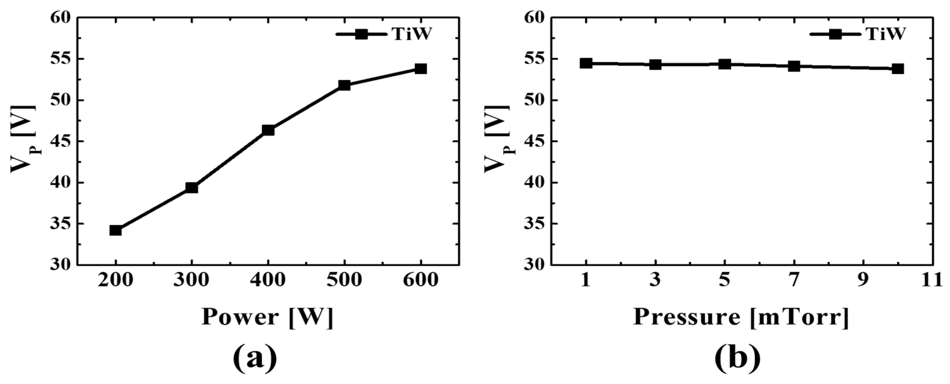
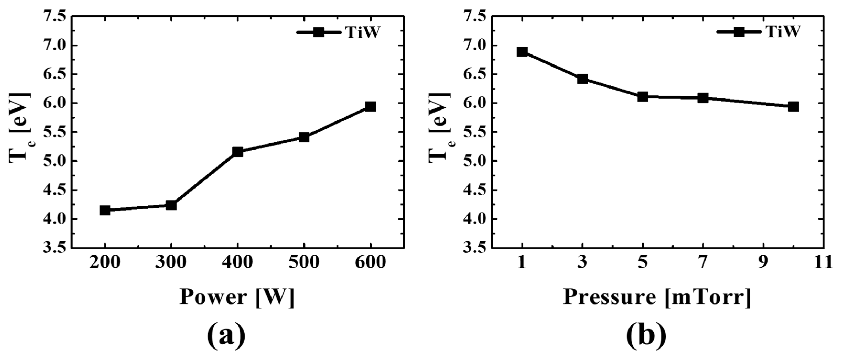
Figure 4, Figure 5 and Figure 6 show the variations in plasma potential (Vp), electron density (ne), and electron temperature (Te) under different applied powers and gas pressures during the RF sputtering process. Under all experimental conditions, the chamber pressure was maintained at 10 mTorr during the applied power variation studies, whereas the applied power was fixed at 600 W during the pressure variation experiments.
R1: Ar + e → Ar+ + 2e (Eth ≈ 15.76 eV)
R2: Ti + e → Ti + + 2e (Eth ≈ 6.82 eV)
R3: W + e → W+ + 2e (Eth ≈ 7.86 eV)
The plasma potential increased linearly with applied power from 200 to 600 W for TiW cases, as shown in Figure 4a. The plasma potential exhibited a relatively large increase of approximately 1.6 times as the applied power was tripled, indicating a strong dependence on the input energy. The plasma potential showed a slight decrease as the process pressure was increased from 1 to 10 mTorr for TiW (Figure 4b), but remained relatively constant overall.
Reactions R1–R3 represent the set of electron-impact ionization processes that occur dominantly in the bulk plasma region during the RF sputtering process [24,26]. The densities of electrons and ions generated in the bulk region are governed predominantly by the Ar ionization process described by R1 and were further influenced by the sputtered Ti or W particle densities near the target. Figure 5a shows the variation in electron density as a function of the applied RF power. As the applied RF power was increased from 200 W to 600 W, the electron density increased by approximately a factor of two. Figure 5b shows the dependence of the electron density on the process pressure. The electron density increased as the pressure was increased, but the variation was less than that induced by changes in applied power.
Figure 6a,b show the electron temperature variations with respect to applied power and process pressure, respectively. The electron energy distribution in the center of the bulk plasma followed a Maxwellian distribution under all operating conditions. As shown in Figure 6a, the electron temperature increased as the applied power increased. This phenomenon occurs because the RF power transfer efficiency improves as the applied power is increased, leading to simultaneous increases in the electron density and electron temperature. In contrast, the electron temperature decreased as the process pressure increased (Figure 6b). This was attributed to the enhanced collisional losses at higher pressures, which result in reduced electron energy under constant power conditions.

3.2. Properties of Sputtered TiW Thin Films

Table 2 lists the variation in the DC negative bias voltage on the sputtering target as a function of the RF power, with the process pressure fixed at 10 mTorr and the substrate temperature maintained at room temperature. In RF discharges with asymmetric electrode configurations, a negative DC self-bias typically develops on the smaller electrode because of the asymmetry in electrode areas. According to Koenig et al., under low-pressure conditions (<10 mTorr), the ratio of the DC bias voltages (V1/V2) across the electrodes with areas A1 and A2 is proportional to (A2/A1)4 [29,30].
In this study, the effective area ratio between the RF-powered target electrode (smaller electrode) and the grounded chamber wall which includes substrate electrode (larger electrode) was approximately 0.05. In a plasma system with asymmetric electrodes, a negative DC self-bias voltage naturally develops on the smaller electrode when driven by an RF power source. This phenomenon arises because the plasma seeks to balance the time-averaged fluxes of electrons and ions to each electrode. Electrons, having much lower mass than ions, respond more rapidly to the RF oscillations and preferentially reach the smaller electrode. To maintain zero net current over an RF cycle, the smaller electrode acquires a negative DC self-bias, which accelerates positive ions toward its surface. This self-bias is a critical parameter in controlling the ion energy and ion bombardment, and thereby strongly influences the microstructure and properties of films deposited in plasma-based processes. As a result, a significant negative DC bias voltage was developed on the target, enabling the sputtering of TiW atoms. The magnitude of the DC bias is influenced by the chamber pressure and the applied RF power and follows the following relationship:
V B     ( P RF / P ) 1 / 2
where V B denotes the absolute value of the self-bias voltage; PRF is the applied RF power; and P is the chamber pressure. During the RF sputtering process, increasing the applied power from 200 W to 600 W (threefold increase) increased V B from 76 V to 129 V. In the case, the increase corresponds approximately to a factor of 3 .
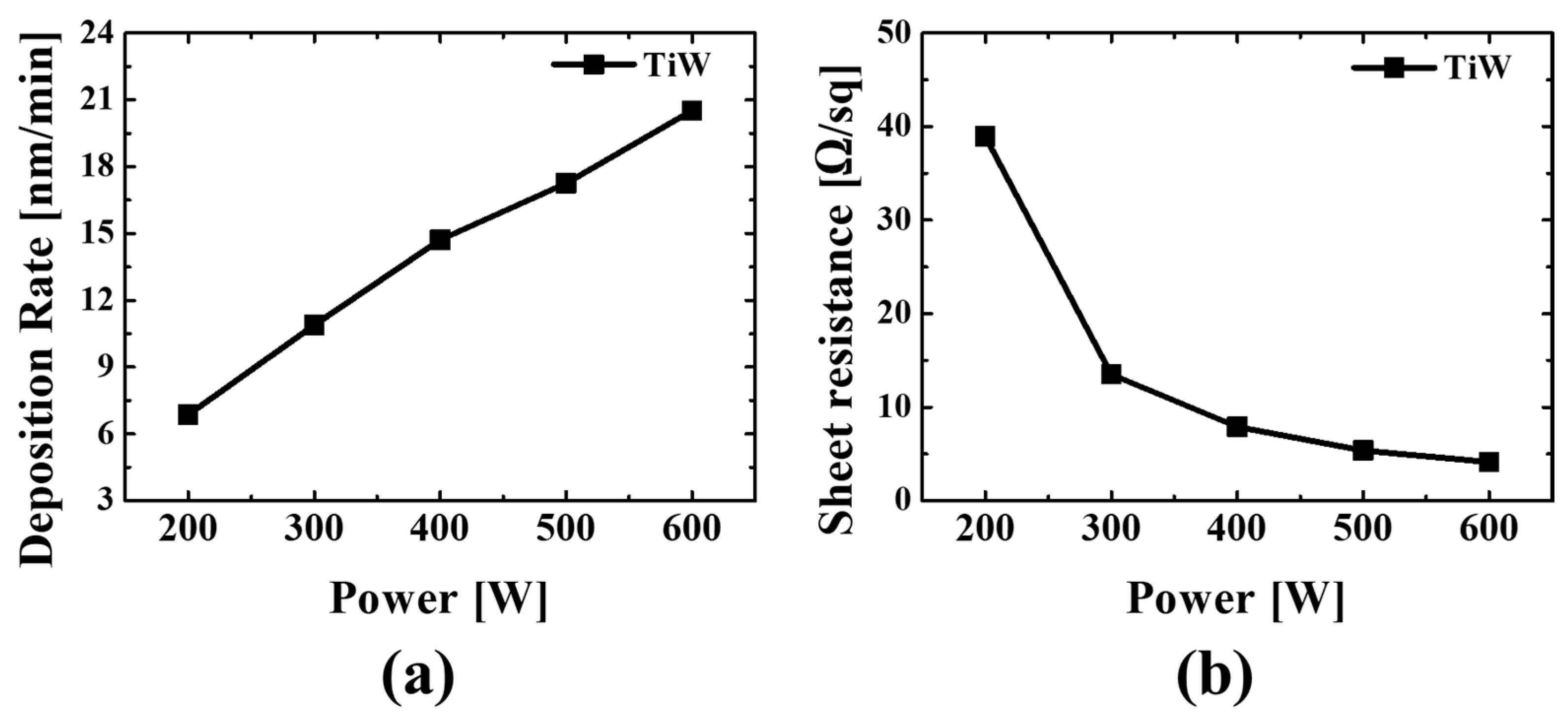
Figure 7 presents the measured deposition rate and sheet resistance [Ω/m2] as a function of the applied RF power under an Ar ambient pressure of 10 mTorr, consistent with the conditions listed in Table 2.
The threshold energy (Eth) required for sputtering by incident ions can be expressed as
E t h > E s b / γ ,       γ = 4 M 1 M 2 ( M 1 + M 2 ) 2
where M1 and M2 represent the masses of the projectile and target atoms, respectively, and Esb denotes the surface binding energy of the target material [29]. For Ti, a single-element target, the threshold energy was approximately 20 eV, suggesting that sputtering initiates when incident ions possess energies above this value. In contrast, TiW is a multicomponent target, and W exhibits a significantly higher threshold energy (~100 eV). For a 1:1 Ti–W alloy composition, sputtering occurs predominantly from Ti atoms (preferential sputtering), and the overall sputtering is observed at ion energies above ~40 eV [18,19,20,21,22,23,24,25,26,27,28,29].
An increase in the DC bias voltage at the powered electrode, where the target is mounted, results in a corresponding increase in the average energy of ions incident on the target. This, in turn, increases the population of high-energy ions in the ion energy distribution. In Ar-based sputtering, the sputtering yield follows a proportional relationship given by
Y     [ 1 ( E t h E i ) 1 / 2 ] s
where Ei, Eth, and s are the incident ion energy, the sputtering threshold energy, and a semi-empirical parameter, respectively [31,32]. Therefore, the increase in ion energy leads to a greater number of atoms being ejected from the target surface.
The plasma potential influences the incident ion energy (Ei) and tends to follow the relation, Ei ∝ ( V p + V B ), where it is approximately proportional to the sum of the plasma potential and the negative DC self-bias voltage. The deposition rate of TiW films increased linearly as the RF power was increased from 200 W to 600 W in 100 W increments in the RF magnetron sputtering process (Figure 7a). According to M.P. Seah et al., in Ar sputtering systems, the sputtering yield increases linearly with the ion energy below 1000 eV and saturates at higher energies [32]. In this study, conducted under RF power levels below 600 W, the maximum DC self-bias voltage ( V B ) observed for the TiW targets ranged from approximately 129 V. This voltage range, combined with the increase in plasma potential with RF power, resulted in a linear increase in deposition rate. Despite relatively higher threshold energy for sputtering in TiW because of its multicomponent composition, TiW exhibits higher deposition rates. This behavior was attributed to its favorable nucleation characteristics derived from the W lattice structure. The self-diffusion coefficients involved in thin film growth were 1.88 × 10⁻⁸ cm2/s for Ti and 6.4 × 10⁻⁸ cm2/s for W [33]. This higher diffusion rate of W atoms enhanced their mobility at the nucleation front, increasing their probability of accumulation on nucleation sites and promoting efficient film growth.
The sheet resistance [Ω/m2] of TiW thin films decreases with increasing RF power (Figure 7b). The sheet resistance is influenced by the intrinsic material properties of Ti and W, as well as by the plasma characteristics during sputtering, and is determined by factors such as film thickness, crystallinity, composition, and defect density. Generally, the sheet resistance is inversely proportional to the film thickness. In RF magnetron sputtering, although the film thickness tends to increase linearly with the applied power, the sheet resistance decreases exponentially [17]. The energetic ions reduce the number of structural defects and improve electrical conductivity. The sheet resistance decreases significantly in the lower power regime (200–400 W) but shows a relatively smaller reduction from 400 W to 600 W. The mechanism of resistance reduction shifts from thickness-driven to density- and defect-related effects as the power increases.
However, in TiW sputtering processes, it is difficult to fully attribute the decrease in resistivity solely to the increase in ion energy. Various factors must be considered, including the crystallographic characteristics of Ti and W during sputter deposition, the reduced surface diffusion caused by low-temperature processing compared to conventional conditions, and the effects of plasma characteristics and deposition rate relative to ion energy under different process parameters. To further investigate these effects, XRD-based analytical methods were applied. The results indicate that the decrease in electrical resistivity is primarily attributed to the reduction in grain boundary density resulting from an increase in grain size.
Figure 8 presents the changes in the crystallinity of TiW thin films as the applied RF power was increased. In RF sputtering, the (110), (200), and (211) peaks at ≈39.5° 2θ, ≈58.3° 2θ, and ≈73.3° 2θ, respectively, were dominant [34,35]. TiW films generally exhibit a body-centered cubic (BCC) structure, with the (110) peak being the most prominent because of the preferred orientation growth influenced by tungsten [31,36]. The relative intensities of these three peaks showed similar ratios under 300 W and 500 W conditions. The 2θ value corresponding to the (200) peak decreased slightly, shifting to the left, indicating an increase in tensile stress caused by the enhanced atomic rearrangements resulting from the increased plasma potential and ion incident energy with rising power [37].
Using X-ray diffraction (XRD) analysis, the variation in lattice quality with applied power was evaluated based on the crystallite size and lattice constant. In the XRD patterns, each diffraction peak ((110), (200), and (211)) ideally appears as a single sharp line; however, in practice, it is observed as a broadened peak due to factors such as crystallite size, microstrain, and instrumental resolution. The full width at half maximum (FWHM, β) quantitatively represents the degree of peak broadening and is defined as the difference in 2θ (theta) between the two points on either side of the peak corresponding to half of the maximum intensity (I_max/2).
X-ray diffraction occurs when X-rays are reflected from atomic planes within a crystal and interfere constructively under specific conditions, producing strong diffraction peaks. This condition is described by Bragg’s law, which is expressed as follows:
n λ = 2 d h k l s i n θ
Here, n denotes the order of reflection, λ is the X-ray wavelength, dhkl is the interplanar spacing of the (hkl) lattice planes, and θ represents the incident angle (Bragg angle). When X-rays are incident on the crystal planes, constructive interference occurs if the path difference in the reflected X-rays is an integer multiple of the X-ray wavelength (λ). Under this condition, strong diffraction peaks are observed at specific 2θ angles by the detector. Using this relationship, the interplanar spacing d h k l of each crystal plane can be calculated inversely from the peak positions (2θ) observed in the XRD pattern.
d h k l = λ 2 sin θ
Therefore, as the 2θ peak shifts to lower angles, θ also decreases, resulting in a decrease in sinθ and, consequently, an increase in the interplanar spacing dhkl. This indicates an expansion of the lattice spacing within the crystal. As shown in Figure 8 and Table 3, the (200) peak of the TiW thin film was observed at 2θ = 57.320° under a 300 W deposition condition and at 2θ = 56.002° under a 500 W condition, corresponding to a Δ2θ of −1.320° (shift toward lower angles). Using Bragg’s law, the (200) interplanar spacing increased from 1.606 Å (at 300 W) to 1.641 Å (at 500 W), yielding a relative change of Δd/d = +2.16%. Considering the BCC structure of TiW, where d = a/2, this corresponds to an increase in the lattice constant (Δa/a = +2.16%), which can be attributed to the relaxation of compressive stress with increasing RF power or an increase in the average lattice constant due to Ti substitution [23].
In general, when the incident ion energy increases during TiW sputtering, the average lattice constant tends to decrease due to Ti resputtering [21] or increase due to compressive stress induced by the ion peening effect. In the present experiment, however, when the process power was increased from 300 W to 500 W, the deposition rate increase due to ion generation was approximately 1.55 times higher than the ion energy increase associated with the elevated plasma potential. As a result, the tensile contribution arising from void formation due to limited surface diffusion in the low-temperature deposition condition dominated over the compressive stress induced by ions.
The crystallite size can be evaluated using the Scherrer equation as follows:
D =   K λ β c o s θ
Here, D represents the crystallite size, λ is the X-ray wavelength, β is the full width at half maximum (FWHM) of the peak, θ is the diffraction angle, and K is the shape factor (0.9). The FWHM of the (200) peak decreased markedly from 0.6025° to 0.3980°, resulting in an increase in the crystallite size calculated using the Scherrer equation from 15.0 nm to 22.6 nm, corresponding to an approximately 50% increase. This indicates a narrowing of the peak width and growth of crystallite size for the (200) diffraction plane.
Table 4 lists the variation in DC negative bias voltage at the target region in TiW sputtering processes, with the RF input power set to 600 W, as a function of the process pressure. In all cases, the absolute value of the bias voltage ( V B ) exhibited inverse proportionality to the square root of the pressure.
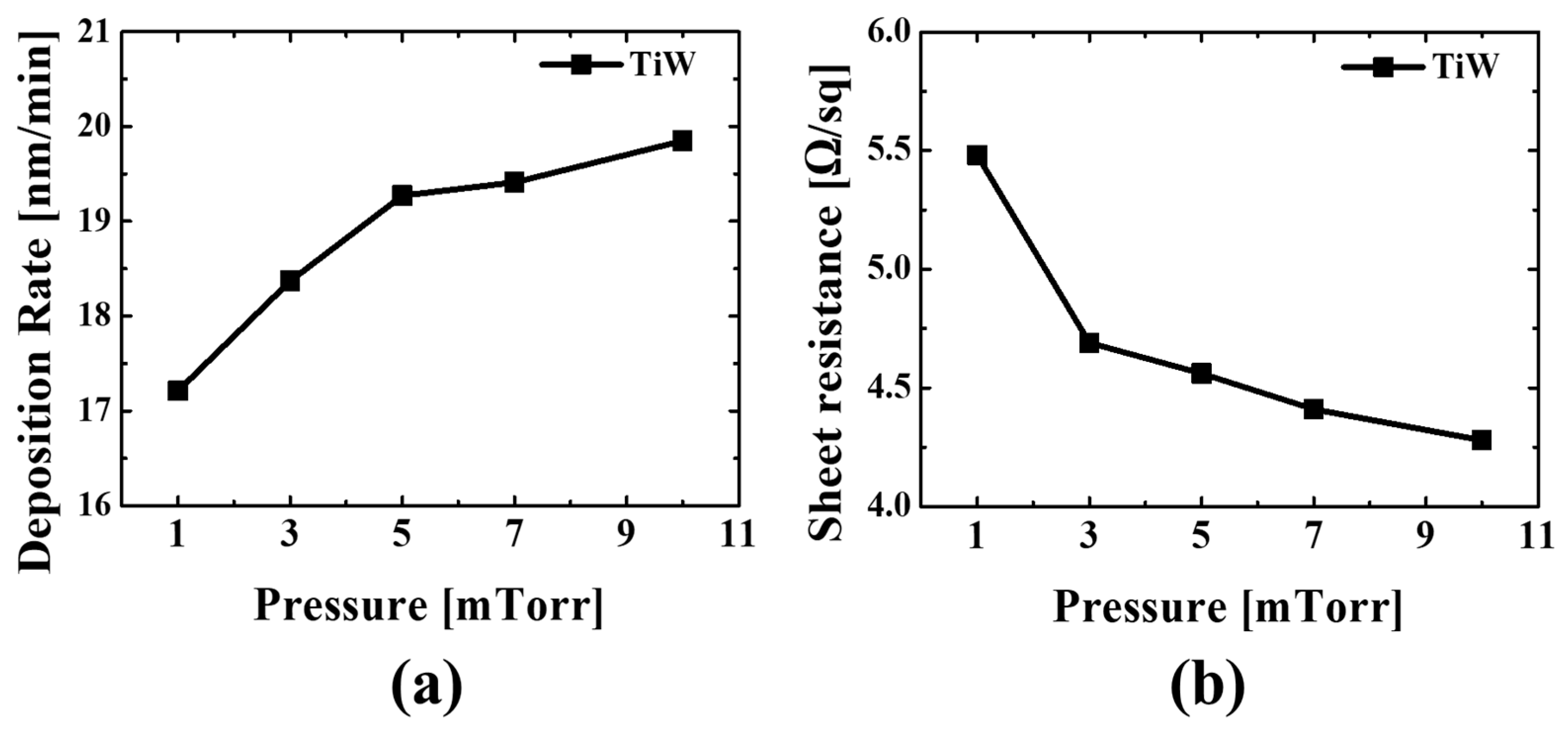
Figure 9a shows the deposition rate at various pressures under a constant RF power of 600 W. The deposition rate increased as the pressure increased. The ion energy incident on the sputtering target is proportional to the sum of the plasma potential and the DC negative bias. The sputtering effect in this regime depends primarily on the ion density because the plasma potential varies only marginally and V B decreases with pressure, as shown in Table 4. As indicated in Figure 5, the increases in electron and ion densities with pressure were smaller than those observed with the changes in input power, resulting in relatively smaller variations in deposition rate.
Figure 9b shows the sheet resistance of the deposited films as a function of the process pressure. The slope of the change in sheet resistance as the pressure was increased was relatively small for TiW. No significant changes in crystallinity were observed in the TiW films with varying pressure, with both maintaining the same crystal structure like in Figure 8. The relatively small changes in sheet resistance with pressure can be attributed to the limited variation in plasma potential and ion density compared to the power-dependent conditions.
Figure 10 presents the variation in the surface roughness of TiW thin films as a function of the applied RF power and process pressure. For TiW films, the maximum surface roughness was observed at 300 W, followed by a linear decrease as the power was increased. Consequently, the incident species have insufficient energy for effective surface migration or atomic rearrangement, leading to increased roughness due to poor surface diffusion. In contrast, at RF powers above 300 W, the deposition promotes denser film growth and a decrease in surface roughness. Figure 10b shows the variation in surface roughness of TiW thin films as a function of the process pressure at a fixed input power of 600 W.
The TiW films showed a decreasing trend in surface roughness with increasing pressure, as shown in Figure 11. Compared to the power variation condition, the effect of pressure on the plasma potential and consequently on the ion energy was relatively minor, resulting in smaller changes in surface roughness.

4. Conclusions

TiW thin films were deposited by low-temperature RF magnetron sputtering with the substrate temperature fixed at room temperature. The changes in bulk plasma characteristics and corresponding thin film properties were investigated as functions of the applied process parameters. The film property variations in TiW were analyzed under different conditions, including the RF input power (200–600 W) and process pressure (1–10 mTorr, with Ar gas) as the main variables. The bulk plasma diagnostics were performed using a Langmuir probe, and the film properties, such as deposition rate, surface roughness, sheet resistance, and crystallinity, were characterized on Si substrates for each set of process conditions.
In the RF magnetron sputtering process of TiW thin films, the deposition rate increased linearly as the applied power increased, while the sheet resistance decreased. Under low-pressure conditions below 10 mTorr, the increase in incident ion energy resulted in the simultaneous enhancement of the sputtering efficiency and deposition rate. Despite its relatively high threshold energy, TiW showed a high deposition rate because of the superior nucleation characteristics of the W-based lattice.
The deposition rates of thin films increased as the process pressure increased. The sputtering effect depended on the ion density, and the changes in plasma potential and ion density with pressure were relatively small compared to variations in applied power, resulting in limited variation in deposition rate. As the pressure increased, the sheet resistance of the TiW films showed gradual decrease. No significant changes in crystallinity were observed for the TiW films with varying pressure. The relatively minor changes in plasma characteristics under pressure variation conditions, compared to those under applied power variations, had limited impact on the electrical properties.
The surface roughness of TiW films exhibited maximum value at 300 W, followed by a linear decrease as the power increased. The surface roughness of TiW films tended to decrease as the pressure increased. Furthermore, under pressure variation conditions, the changes in plasma potential and ion density were smaller than those under varying power, resulting in limited variations in surface roughness.

Author Contributions

Conceptualization, C.B. and J.-H.C.; methodology, J.-H.C.; validation, C.B. and J.-H.C.; formal analysis, C.Y.J.; investigation, C.B. and C.Y.J.; resources, J.-H.C.; data curation, C.B.; writing—original draft preparation, C.B. and J.-H.C.; writing—review and editing, J.-H.C.; visualization, C.Y.J.; supervision, J.-H.C.; project administration, J.-H.C.; funding acquisition, J.-H.C. All authors have read and agreed to the published version of the manuscript.

Funding

This work was supported by the Technology Innovation Program (Grant No. RS-2023-00265582, Development of monitoring and analysis technologies for greenhouse gases in the semiconductor manufacturing etching process) funded by the Ministry of Trade, Industry & Energy [MOTIE, Korea (Grant No. 1415188192)].

Institutional Review Board Statement

Not applicable.

Informed Consent Statement

Not applicable.

Data Availability Statement

The data presented in this study are available on request from the corresponding author.

Acknowledgments

RF sputtering process was performed with a multi-target sputtering system at Gyeongsang National University.

Conflicts of Interest

The authors declare no conflicts of interest.

References

  1. Beyne, E.; De Moor, P.; Ruythooren, W.; Labie, R.; Jourdain, A.; Tilmans, H.; Tezcan, D.S.; Soussan, P.; Swinnen, B.; Cartuyvels, R. Through-Silicon via and Die Stacking Technologies for Microsystems-Integration. In Proceedings of the 2008 IEEE International Electron Devices Meeting, San Francisco, CA, USA, 15–17 December 2008; pp. 1–4. [Google Scholar]
  2. Gambino, J.P.; Adderly, S.A.; Knickerbocker, J.U. An Overview of Through-Silicon-via Technology and Manufacturing Challenges. Microelectron. Eng. 2015, 135, 73–106. [Google Scholar] [CrossRef]
  3. Knickerbocker, J.U.; Andry, P.S.; Dang, B.; Horton, R.R.; Patel, C.S.; Polastre, R.J.; Sakuma, K.; Sprogis, E.S.; Tsang, C.K.; Webb, B.C. 3D Silicon Integration. In Proceedings of the 2008 58th Electronic Components and Technology Conference, Lake Buena Vista, FL, USA, 27–30 May 2008; pp. 538–543. [Google Scholar]
  4. Diehl, D.; Kitada, H.; Maeda, N.; Fujimoto, K.; Ramaswami, S.; Sirajuddin, K.; Yalamanchili, R.; Eaton, B.; Rajagopalan, N.; Ding, R.; et al. Formation of TSV for the Stacking of Advanced Logic Devices Utilizing Bumpless Wafer-on-Wafer Technology. Microelectron. Eng. 2012, 92, 3–8. [Google Scholar] [CrossRef]
  5. Zhang, W. Fine Pitch Cu/Sn Solid State Diffusion Bonding for Advanced Three-Dimensional Chip Stacking. Jpn. J. Appl. Phys. 2015, 54, 030203. [Google Scholar] [CrossRef]
  6. Burns, J.; Stucchi, M.; Patti, R.; Cong, J.; Lee, Y.-J.; Milojevic, D.; Carlson, D.; Xie, Y.; Vardaman, E.-J. Three Dimensional System Integration: IC Stacking Process and Design; Papanikolaou, A., Soudris, D., Radojcic, R., Eds.; Springer: New York, NY, USA, 2011. [Google Scholar]
  7. Banerjee, K.; Souri, S.J.; Kapur, P.; Saraswat, K.C. 3-D ICs: A Novel Chip Design for Improving Deep-Submicrometer Interconnect Performance and Systems-on-Chip Integration. Proc. IEEE 2001, 89, 602–633. [Google Scholar] [CrossRef]
  8. Knickerbocker, J.U.; Patel, C.S.; Andry, P.S.; Tsang, C.K.; Buchwalter, L.P.; Sprogis, E.J.; Gan, H.; Horton, R.R.; Polastre, R.J.; Wright, S.L. 3-D Silicon Integration and Silicon Packaging Technology Using Silicon Through-Vias. IEEE J. Solid-State Circuits 2006, 41, 1718–1725. [Google Scholar] [CrossRef]
  9. Lau, J.H. Overview and Outlook of Three-Dimensional Integrated Circuit Packaging, Three-Dimensional Si Integration, and Three-Dimensional Integrated Circuit Integration. J. Electron. Packag. 2014, 136, 040801. [Google Scholar] [CrossRef]
  10. Wei, T.; Cai, J.; Wang, Q.; Hu, Y.; Wang, L.; Liu, Z.; Wu, Z. Optimization and Evaluation of Sputtering Barrier/Seed Layer in through Silicon via for 3-D Integration. Tsinghua Sci. Technol. 2014, 19, 150–160. [Google Scholar] [CrossRef]
  11. Schmitz, J. Low Temperature Thin Films for Next-Generation Microelectronics. Surf. Coat. Technol. 2018, 343, 83–88. [Google Scholar] [CrossRef]
  12. Cheemalamarri, H.K.; Senthilkumar, D.; Rao, B.S.S.C. Through Silicon Via Oxide Etch Back for Via-Last Integration Scheme. In Proceedings of the 2022 IEEE 24th Electronics Packaging Technology Conference (EPTC), Singapore, 7–9 December 2022; pp. 973–976. [Google Scholar]
  13. Garrou, P.; Bower, C.; Roozeboon, F.; Lamy, Y.; Chang, S.-M.; Wieland, R.; Ritzdorf, T. Handbook of 3D Integration: Technology and Applications of 3D Integrated Circuits; Garrou, P., Ed.; Wiley-VCH: Weinheim, Germany, 2014. [Google Scholar]
  14. Sakata, A.; Yamashita, S.; Omoto, S.; Hatano, M.; Wada, J.; Higashi, K.; Yamaguchi, H.; Yosho, T.; Imamizu, K.; Yamada, M.; et al. Reliability Improvement by Adopting Ti-Barrier Metal for Porous Low-k ILD Structure. AIP Conf. Proc. 2007, 945, 98–106. [Google Scholar]
  15. Jiang, T.; Im, J.; Huang, R.; Ho, P.S. Through-Silicon via Stress Characteristics and Reliability Impact on 3D Integrated Circuits. MRS Bull. 2015, 40, 248–256. [Google Scholar] [CrossRef]
  16. Wu, W.; Wu, H.-J.; Dixit, G.; Shaviv, R.; Gao, M.; Mountsier, T.; Harm, G.; Dulkin, A.; Fuchigami, N.; Kailasam, S.K. Ti-Based Barrier for Cu Interconnect Applications. In Proceedings of the 2008 International Interconnect Technology Conference, Burlingame, CA, USA, 1–4 June 2008; pp. 202–204. [Google Scholar]
  17. Bang, C.; Cha, J.-H. Properties of Titanium Thin Film Deposited by RF and DC Magnetron Sputtering at Low Temperatures. AIP Adv. 2025, 15, 065105. [Google Scholar] [CrossRef]
  18. Wasa, K.; Motohiro, T.; Adachi, H.; Tominaga, K.; Matsushima, K. Handbook of Sputter Deposition Technology: Fundamentals and Applications for Functional Thin Films, Nano-Materials and MEMS; Wasa, K., Kanno, I., Koetera, H., Eds.; William Andrew: New York, NY, USA, 2012. [Google Scholar]
  19. Ensinger, W. Low Energy Ion Assist during Deposition—An Effective Tool for Controlling Thin Film Microstructure. Nucl. Instrum. Methods Phys. Res. Sect. B Beam Interact. Mater. At. 1997, 127, 796–808. [Google Scholar] [CrossRef]
  20. Loch, D.A.L.; Ehiasarian, A.P. Study of the Effect of RF-Power and Process Pressure on the Morphology of Copper and Titanium Sputtered by ICIS. Surf. Coat. Technol. 2017, 327, 200–206. [Google Scholar] [CrossRef]
  21. Saghaeian, F.; Keckes, J.; Woehlert, S.; Rosenthal, M.; Reisinger, M.; Todt, J. Microstructure and Stress Gradients in TiW Thin Films Characterized by 40 nm X-Ray Diffraction and Transmission Electron Microscopy. Thin Solid Films 2019, 691, 137576. [Google Scholar] [CrossRef]
  22. Kalha, C.; Reisinger, M.; Thakur, P.; Lee, T.-L.; Venkatesan, S.; Isaacs, M.; Nelhiebel, M.; Regoutz, A. Evaluation of the thermal stability of TiW/Cu heterojunctions using a combined SXPS and HAXPES approach. J. Appl. Phys. 2022, 131, 165301. [Google Scholar] [CrossRef]
  23. Glebovsky, V.G.; Yaschak, V.Y.; Baranov, V.V.; Sackovich, E.L. Properties of titanium-tungsten thin films obtained by magnetron sputtering of composite cast targets. Thin Solid Films 1995, 257, 1–6. [Google Scholar] [CrossRef]
  24. Pflug, A.; Siemers, M.; Schwanke, C.; Febty Kurnia, B.; Sittinger, V.; Szyszka, B. Simulation of Plasma Potential and Ion Energies in Magnetron Sputtering. Mater. Technol. 2011, 26, 10–14. [Google Scholar] [CrossRef]
  25. Kaltofen, R.; Sebald, T.; Weise, G. Ion Bombardment Diagnostics in a Nitrogen RF Magnetron Sputtering Discharge. Surf. Coat. Technol. 1997, 97, 131–139. [Google Scholar] [CrossRef]
  26. Han, J.G. Recent Progress in Thin Film Processing by Magnetron Sputtering with Plasma Diagnostics. J. Phys. D Appl. Phys. 2009, 42, 043001. [Google Scholar] [CrossRef]
  27. Lieberman, M.A.; Lichtenberg, A.J. Principles of Plasma Discharges and Materials Processing, 2nd ed.; John Wiley & Sons: Hoboken, NJ, USA, 2005. [Google Scholar]
  28. Kim, S.-W.; Cha, J.-H.; Jung, S.-H.; Shim, S.; Kim, C.H.; Lee, H.-J. Characteristics of Segmented Dielectric Window Inductively Coupled Plasma. AIP Adv. 2023, 13, 045022. [Google Scholar] [CrossRef]
  29. Behrisch, R.; Eckstein, W. Sputtering by Particle Bombardment: Experiments and Computer Calculations from Threshold to MeV Energies; Springer: Berlin, Germany, 2007. [Google Scholar]
  30. Koenig, H.R.; Maissel, L.I. Application of RF Discharges to Sputtering. IBM J. Res. Dev. 1970, 14, 168–171. [Google Scholar] [CrossRef]
  31. Grill, A. Cold Plasma in Materials Fabrication: From Fundamentals to Applications; IEEE Press: Piscataway, NJ, USA, 1994. [Google Scholar]
  32. Seah, M.P.; Clifford, C.A.; Green, F.M.; Gilmore, I.S. An accurate semi-empirical equation for sputtering yields I: For argon ions. Surf. Interface Anal. 2005, 37, 444–458. [Google Scholar] [CrossRef]
  33. Petrović, S.; Bundaleski, N.; Peruško, D.; Radović, M.; Kovač, J.; Mitrić, M.; Gaković, B.; Rakočević, Z. Surface Analysis of the Nanostructured W–Ti Thin Film Deposited on Silicon. Appl. Surf. Sci. 2007, 253, 5196–5202. [Google Scholar] [CrossRef]
  34. Jeyachandran, Y.L.; Karunagaran, B.; Narayandass, S.K.; Mangalaraj, D.; Jenkins, T.E.; Martin, P.J. Properties of Titanium Thin Films Deposited by Dc Magnetron Sputtering. Mater. Sci. Eng. A 2006, 431, 277–284. [Google Scholar] [CrossRef]
  35. Oparowski, J.M.; Sisson, R.D.; Biederman, R.R. The Effects of Processing Parameters on the Microstructure and Properties of Sputter-Deposited TiW Thin Film Diffusion Barriers. Thin Solid Films 1987, 153, 313–328. [Google Scholar] [CrossRef]
  36. Liu, D.; Dew, S.K.; Brett, M.J.; Smy, T.; Tsai, W. Compositional Variations in Ti-W Films Sputtered over Topographical Features. J. Appl. Phys. 1994, 75, 8114–8120. [Google Scholar] [CrossRef]
  37. Le Priol, A.; Le Bourhis, E.; Renault, P.-O.; Muller, P.; Sik, H. Structure-Stress-Resistivity Relationship in WTi Alloy Ultra-Thin and Thin Films Prepared by Magnetron Sputtering. J. Appl. Phys. 2013, 113, 213504. [Google Scholar] [CrossRef]
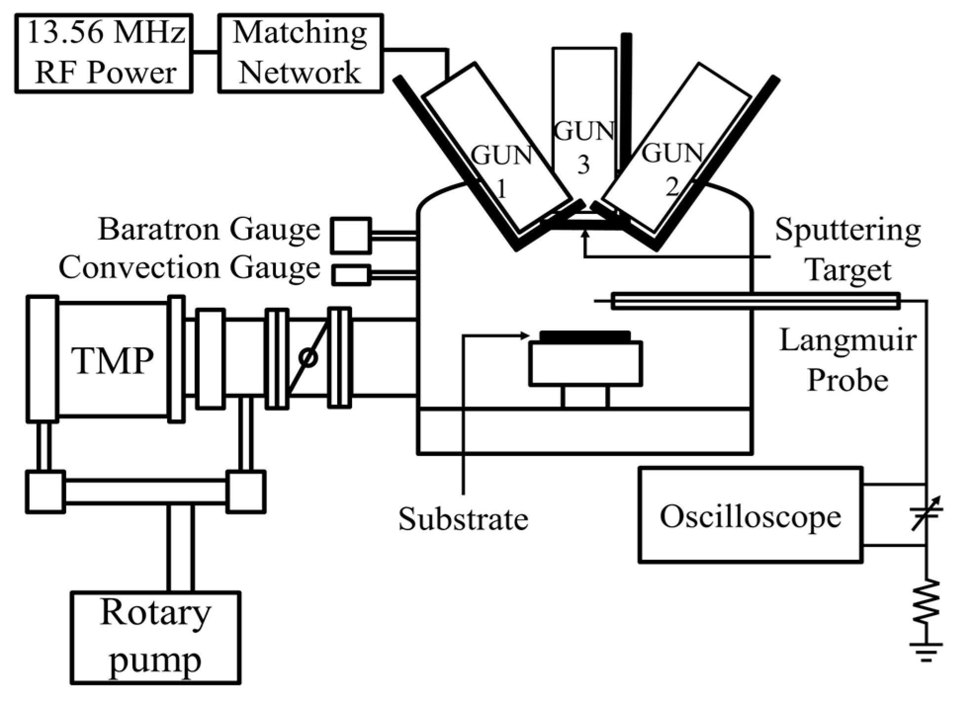
Figure 1. Schematic diagram of RF magnetron sputtering and Langmuir probe diagnostic system.
Applsci 15 12300 g001
Figure 2. Schematic diagram of the sputtering chamber: (a) Front view; (b) Top view.
Applsci 15 12300 g002
Figure 3. Schematic of a single Langmuir probe.
Applsci 15 12300 g003
Figure 4. Plasma potential measured using a Langmuir probe as a function of the process parameters: (a) Input power; (b) Process pressure.
Applsci 15 12300 g004
Figure 5. Electron density measured using a Langmuir probe as a function of the process parameters: (a) Input power; (b) Process pressure.
Applsci 15 12300 g005
Figure 6. Electron temperature measured using a Langmuir probe as a function of the process parameters: (a) Input power; (b) Process pressure.
Applsci 15 12300 g006
Figure 7. Titanium–tungsten alloy film properties according to the input power: (a) Deposition rate; (b) Sheet resistance.
Applsci 15 12300 g007
Figure 8. XRD patterns of TiW thin film according to input power.
Applsci 15 12300 g008
Figure 9. Titanium–tungsten alloy film properties according to the process pressure: (a) Deposition rate; (b) Sheet resistance.
Applsci 15 12300 g009
Figure 10. Surface roughness of titanium–tungsten alloy film according to the process parameters: (a) Input power; (b) Process pressure.
Applsci 15 12300 g010
Figure 11. Three-dimensional AFM images of titanium–tungsten alloy films sputtered at various pressures: (a) 1 mTorr; (b) 5 mTorr; (c) 10 mTorr.
Applsci 15 12300 g011
Table 1. Experimental conditions for magnetron sputtering.
Sputtering
Target
Operation
Frequency
Ar Gas Flow
[sccm]
Power
[W]
Pressure
[mTorr]
TiW13.56 MHz RF302001
3003
4005
5007
60010
Table 2. Self-bias conditions of the titanium–tungsten alloy target according to the input power.
Sputtering
Target
Operation
Frequency
Power
[W]
Pressure
[mTorr]
Negative DC
Voltage [V]
TiW13.56 MHz RF20010−76
300−92
400−106
500−119
600−129
Table 3. 2θ positions, FWHM, and crystallite sizes (Dscherrer) were obtained using Scherrer and Williamson–Hall (WH) analyses.
Input PowerPeak2theta [°]FWHM [°]DScherrer [nm]
300(110)39.6200.528515.98
(200)57.3200.602515.03
(211)72.0200.486420.19
600(110)39.5400.511816.50
(200)56.0020.398022.61
(211)72.0200.511019.22
Table 4. Self-bias conditions of titanium–tungsten alloy target according to the process pressure.
Sputtering
Target
Operation
Frequency
Power
[W]
Pressure
[mTorr]
Negative DC
Voltage [V]
TiW13.56 MHz RF6001−169
3−158
5−144
7−136
10−129
Disclaimer/Publisher’s Note: The statements, opinions and data contained in all publications are solely those of the individual author(s) and contributor(s) and not of MDPI and/or the editor(s). MDPI and/or the editor(s) disclaim responsibility for any injury to people or property resulting from any ideas, methods, instructions or products referred to in the content.