1. Introduction
The in-depth application of ultrasonic testing technology in the aerospace, petroleum, and chemical industries has imposed stringent requirements on high-speed signal processing. With the evolution of electronic technology toward high frequency and high speed, the problem of current mutation caused by simultaneous switching of multiple pins in digital circuits has become increasingly prominent. When a large number of signal lines switch logic states simultaneously, transient current couples through the parasitic parameters of the power/ground network and generates significant SSN [
1]. Essentially, this noise is the electromagnetic response of the parasitic inductance in the PDN to the transient current. The voltage fluctuation caused by SSN directly degrades signal integrity, induces timing jitter, and even leads to system functional failure.
In high-frequency scenarios, increased chip integration and faster signal edge rates further amplify the SSN effect. For instance, a nanosecond-level rising edge exhibits a current slew rate of hundreds of amperes per second; its interaction with picohenry-scale package parasitic inductance induces a voltage dip of tens of millivolts at the power pin—far exceeding the noise margin of low-voltage digital circuits. Especially in the ultrasonic testing field where high signal accuracy is required, the power fluctuation caused by SSN severely affects the signal-to-noise ratio of echo signal acquisition and reduces the defect identification capability [
2]. Therefore, in-depth analysis of the SSN generation mechanism and the establishment of an efficient suppression strategy have become key technical issues to ensure the stable operation of high-speed electronic systems.
The generation of SSN is closely related to the impedance characteristics of the PDN and inductive coupling at the chip level. In high-speed digital circuits, low core voltage, high integration, and fast edge rate intensify the current transient (di/dt), causing the PDN impedance to resonate at specific frequency bands. A voltage fluctuation at the millivolt level can trigger logic errors. Traditional suppression methods such as decoupling capacitors can reduce medium- and low-frequency noise, but their self-resonant frequency (SRF) limitation (usually below 600 MHz) makes them ineffective in dealing with GHz-level high-frequency SSN. In addition, the parasitic inductance in chip packaging and PCB layout further amplifies the mutual inductive coupling effect between I/Os, requiring systematic suppression through electromagnetic compatibility design optimization and algorithm integration.
In the field of SSN suppression, domestic scholars have focused on electromagnetic bandgap (EBG) structures and PCB design optimization. Sun et al. proposed a hybrid embedded EBG structure, which significantly suppresses SSN through ultra-wideband stopband design (370 MHz–20 GHz) with less than 5% impact on the signal eye diagram [
3]. Chen’s team developed a CBS-EBG structure with C-type bridging and slotting design, extending the stopband to 296 MHz–15 GHz while maintaining signal integrity [
4]. Wang innovatively etched EBG units on microstrip lines and verified their strong suppression capability for SSN in baseband signals [
5]. Lu achieved ultra-wideband suppression (150 MHz–10.7 GHz) through a branch-wound unit patch design and optimized the signal path through differential transmission [
6]. In terms of PCB design, Luo proposed an SSN analytical method based on time-domain convolution, simplifying the frequency-domain calculus of impedance function and switching current to provide a fast noise evaluation tool for 3D chip stacking design [
7]. Li developed an SSN reliability testing method for high-speed PCBs, optimizing the decoupling capacitor configuration by combining temperature stress experiments and impedance analysis [
8]. Yu optimized the PDN design using the target impedance method from the perspective of PI and verified the effectiveness of the decoupling scheme through Ansoft tools [
9].
International scholars have focused on model construction and system-level optimization. Dong et al. proposed a PI prediction framework based on Convolutional Neural Network (CNN), realizing efficient analysis of dynamic noise and voltage surges through spatiotemporal compression technology [
10]. Xu’s team developed a simplified CPM-PDN joint model, combining the characteristics of weak-signal Voltage Regulator Module (VRM) to provide a new method for system-level transient PI analysis [
11]. Liu et al. systematically discussed the relationship between decoupling capacitor placement and crosstalk coupling, proposing a frequency-divided decoupling strategy to reduce power noise [
12]. Zhao et al. reduced the parasitic inductance using a Smart Power Stage (SPS) chip structure for buck converters, reducing the switching noise amplitude by 40% [
13]. Park compared the loop model and Partial Element Equivalent Circuit (PEEC) model, pointing out the latter’s accuracy advantage in simulating large currents in DDR5 ground rails [
14]. Zhang and Liu proposes an improved mode tracking algorithm to address the mode-mixing problem in broadband RLGC parameter extraction for multi-conductor transmission lines [
15], this method enhances the accuracy and stability of the parameter model. Lin studies a power and ground bridging routing design for improving power integrity [
16], this design reduces the impedance of the power distribution network by optimizing the current path. Kumar and Sitaraman addressed PDN resonance issues in three-dimensional glass interposer packaging [
17] by proposing a resonance suppression scheme based on double-sided vertical interconnect structures. By optimizing the layout of through-glass vias (TGVs) and designing electromagnetic bandgaps, they effectively reduced power/ground noise propagation, providing experimental validation for high-frequency stability in high-density integrated systems. To further improve PDN impedance adaptability, Xu and Bai proposed a hybrid target impedance model [
18], dynamically adjusting optimization goals by integrating frequency-domain impedance characteristics with time-domain noise tolerance, significantly enhancing PDN stability across a wide bandwidth, particularly suited for non-uniform load scenarios. Facing the challenge of optimizing complex multi-port PDNs, Wang and Xu introduced a Newton–Hessian minimization method [
19], achieving efficient high-dimensional gradient descent optimization by precisely calculating the second-order derivatives of the impedance matrix. This approach resolves the tendency of traditional heuristic algorithms to converge to local optima, significantly improving convergence accuracy and speed for large-scale networks. While ensuring electrical performance, economic constraints are equally important. Xu et al. incorporated both timing jitter control and cost factors into the optimization objectives [
20], proposing a PDN economic optimization framework based on multi-objective genetic algorithms, which for the first time minimized hardware overhead—such as the number and layout area of decoupling capacitors—while suppressing power-induced timing jitter, providing a new approach for low-cost design of high-performance integrated circuits. Chang et al. were the first to incorporate power-induced jitter into target impedance modeling [
21], proposing a Chip-Pkg-PCB co-signoff flow that overcomes the traditional model’s limitations of “emphasizing ripple while neglecting timing”. Addressing the heterogeneous characteristics of chiplet-based 2.5D integrated circuits, Zhi, CL, and Dong, G proposed a compromise-oriented impedance optimization method driven by a hybrid MDP algorithm, effectively balancing noise suppression with layout constraints [
22]. As 2.5D/3D integration density increases, the coupling between thermal effects and electrical performance becomes increasingly prominent. Wang, Y, and Zhi, CL innovatively integrated TTSV cooling functionality with PDN optimization, establishing an electrothermal co-design framework that provides cross-physical-domain solutions for high-density integrated systems [
23].
Despite the various SSN suppression strategies and achievements proposed by many scholars and researchers, there are still shortcomings: insufficient high-frequency suppression capability (traditional methods rely on single-capacitance capacitors, and Self-resonant frequency SRF has difficulty covering GHz-level wideband noise), significant influence of parasitic parameters, low multi-objective optimization efficiency, and performance bottlenecks of optimization algorithms. For example, traditional algorithms have slow convergence: the genetic algorithm (GA) requires a large number of iterations (>500) to optimize capacitor placement and is prone to local optimization; machine learning models have weak interpretability: although CNN can predict PDN impedance, it cannot provide physical guidance for capacitor selection.
To address the shortcomings of insufficient high-frequency suppression capability and low multi-objective optimization efficiency in traditional SSN suppression, this paper achieves a systematic breakthrough through the collaborative application of the Sigrity toolchain and SOA:
A high-precision PDN impedance model is constructed using Sigrity frequency-domain S-parameter extraction and Sigrity time-domain simulation to accurately quantify package inductance (e.g., 1 nH) and the GHz-level switching current spectrum, solving the problem of insufficient characterization of parasitic parameters by traditional empirical formulas.
The Sigrity Resonance Analysis module is used to locate planar resonance peaks (e.g., 200 MHz impedance peak) and a layered decoupling network is used to expand the low-impedance frequency band to 50 MHz–1 GHz, breaking the suppression limitation of single capacitors in the high-frequency band.
The spiral flight mechanism and attack phase of SOA are used for collaborative optimization, which improves the convergence speed compared with the Particle Swarm Optimization (PSO) algorithm and avoids falling into local optimization. Meanwhile, a multi-objective function (fitness = 0.4 × impedance + 0.3 × frequency coverage + 0.2 × cost + 0.1 × spacing) is used to optimize SSN, providing a quantifiable engineering path for PI and SSN design in high-density digital systems.
2. SSN Generation and Suppression Mechanism
Simultaneous switching noise (SSN) is a critical power integrity (PI) issue in high-speed digital circuits [
15]. It essentially refers to the noise caused by current mutation in power and ground lines when multiple output drivers switch states simultaneously. In digital circuits, when a large number of I/O pins switch from high level to low level (or vice versa) simultaneously, the transient current ΔI generates a voltage drop
across the parasitic inductance
L of the power distribution network (PDN), leading to voltage fluctuation in power and ground planes. This noise not only degrades signal integrity (SI) but also induces timing jitter, increases the bit error rate, and even causes system failure [
16]. The following sections introduce the theoretical modeling of SSN and the suppression mechanism of decoupling capacitors.
2.1. Multi-Physical Field Coupling Model of SSN
Basic Physical Model
The essence of SSN can be traced back to the electromagnetic response of the parasitic inductance in the PDN to the transient current. According to Faraday’s law of electromagnetic induction, the voltage drop generated by the current mutation across the inductive component is expressed as
where L is the distributed inductance of the PDN path (H), and
is the current change rate caused by driver switching (A/s). This model reveals the electromagnetic nature of SSN generation, i.e., the spatiotemporal coupling effect between transient current and parasitic inductance, which causes voltage fluctuation in power and ground planes and further affects circuit performance.
To address this issue, decoupling capacitors serve as an effective means to suppress SSN. By introducing a decoupling capacitor C into the PDN, an LC low-pass filter network can be constructed with the parasitic inductance L. Compared with the pure inductive path, this network exhibits significant advantages in the high-frequency band: the capacitive reactance
decreases with increasing frequency, while the inductive reactance
increases with increasing frequency. The interaction between the two enables the capacitive reactance to effectively offset the inductive reactance. Through this complementary characteristic, the equivalent impedance of the PDN is significantly reduced, thereby effectively suppressing the SSN problem caused by excessive impedance and providing a more stable power supply environment for the circuit.
2.2. Time-Domain Model of Single-Driver Switching
Assume that the driver current jumps from 0 to I
max within the rise time t
r; the equivalent current change rate is
The corresponding voltage noise is
This model indicates that the noise amplitude is positively correlated with the current change rate and path inductance. By providing local charge storage, the decoupling capacitor can shorten the current loop length, thereby reducing the effective inductance L and further lowering the noise.
2.3. Superposition Model of Multi-Driver Collaborative Switching
When N drivers switch in parallel, the total noise voltage is the linear superposition of the inductive voltage drops of each channel:
When considering the difference in distributed inductance, the total noise depends on the independent contribution of each channel. Through the near-end coupling of high-frequency capacitors (spacing < 5 mm), the noise decoupling of each channel can be achieved. The transient response characteristic of the capacitor (τ = RC < 1 ns) ensures that the current mutation of multiple channels is absorbed locally, avoiding global noise superposition.
2.4. Frequency-Domain Impedance Analysis and Design Criteria
2.4.1. PDN Frequency-Domain Impedance Model
The equivalent impedance of the PDN is jointly determined by the distributed resistance R, inductance L, and decoupling capacitor C:
at the resonant frequency
The impedance reaches a minimum value, and the noise amplification effect is significant.
By paralleling multiple capacitors (e.g., 0.01 μF + 1 μF combination), the low-impedance frequency band can be expanded. The self-resonant frequency (SRF) of the capacitor should cover the main frequency component of the driver switching noise, with a typical engineering value of 50 MHz–1 GHz.
2.4.2. Frequency-Domain Expression of Noise Voltage
The noise spectrum is determined by the product of the Fourier transform I(f) of the driver current and the PDN impedance:
Near the resonant frequency, the noise amplitude can be enhanced by more than 10 dB. The capacitive impedance (1/j2πfC) dominates the PDN characteristics in the high-frequency band, making Z_PDN(f) exhibit a capacitive attenuation characteristic. The introduction of decoupling capacitors can reduce the impedance, thereby achieving noise suppression.
2.5. Time-Domain Response and Peak Voltage Control
2.5.1. Time-Domain Integration for Step-Current Excitation
For an ideal step current,
the time-domain noise voltage is obtained through convolution integration:
This integral captures the transient response of the power delivery network (PDN) impedance to the abrupt change in current.
2.5.2. Peak Voltage Prediction Model
The peak noise voltage during simultaneous switching is given by
This equation explicitly defines the linear relationship between the peak noise voltage and the inductance L, resistance R, and current slew rate.
Advantages of Decoupling Capacitance Suppression
Ztarget ≤ Vripple/Imax is achieved through capacitor configuration, ensuring the PDN impedance remains below the required threshold across the frequency spectrum.
- 2.
Current Bypassing:
High-frequency capacitors provide low-inductance paths, effectively diverting high-frequency noise and reducing di/dt.
- 3.
Resonance Suppression:
The total capacitance value for critical frequency bands (f
res) must satisfy
This ensures that resonant peaks are effectively suppressed, maintaining stability in the power distribution network.
3. Experiment Simulation
The PCB stackup parameters are shown in the
Figure 1 below.
In the field of high-speed circuit design, simultaneous switching noise (SSN) has become a key bottleneck limiting system performance. Its essence lies in the complex electromagnetic interactions excited within the power distribution network (PDN) by transient currents induced by synchronous switching of digital devices. To systematically deconstruct the generation and propagation mechanisms of SSN and develop effective suppression strategies, it is essential to leverage the collaborative capabilities of multi-dimensional analysis techniques within the Sigrity toolchain. These core technologies, including power–ground noise simulation, S-parameter evaluation, power noise metrics, resonance analysis, and noise coupling analysis, form an interrelated and complementary system.
PCB Stackup Detailed Design: This study adopts a 10-layer symmetric FR-4 substrate stackup, with the core design goal of balancing high-speed signal integrity (SI), power integrity (PI), and mechanical stability. Through the alternating layout and symmetrical design of “signal layer–power layer–ground layer,” parasitic inductance and interlayer noise coupling are minimized, providing an optimized physical structure foundation for synchronous switching noise (SSN) suppression. The detailed parameters and functional design of the stackup are as follows, from top to bottom: Layer 1 is the top signal layer, made of FR-4 material with a thickness of 0.076 mm and a typical dielectric constant of 4.2 at the 1 GHz frequency band (measured value 4.15), with a copper foil thickness of 1 oz. It is mainly used for routing high-frequency signals such as CPU/GPU high-speed I/Os. During layout, the projection areas of the underlying power layer should be avoided to reduce coupling interference between signals and the power network. Layer 2 is the power layer (PWR06), with FR-4 material thickness of 0.102 mm, the same dielectric constant as the top signal layer, and copper foil thickness of 2 oz. It serves as the primary distribution layer for the 1.2 V core power supply and forms a “power–ground” coupling pair with the adjacent Layer 3 ground layer (GND09), effectively reducing the parasitic inductance of the power distribution network (PDN). Layer 3 is the ground layer (GND09). The parameters are completely consistent with the second-layer power plane, serving the function of signal return. They form stable return paths with the top-layer signal layer (Layer 1) and the power layer (Layer 2), further optimizing the PDN impedance characteristics. The fourth layer is an inner signal layer, made of FR-4 material with a thickness of 0.076 mm and copper foil thickness of 1oz, used for routing low-speed control signals and other auxiliary traces. During design, it is necessary to avoid the resonance areas of the power/ground layers to prevent noise coupling. The fifth layer is a ground plane (GND07), with parameters consistent with other ground layers, paired with the sixth-layer backup power plane as the return path to suppress cross-layer power noise propagation. The sixth layer is a power plane (PWR06), structurally identical to the second-layer main power plane, used for distributing 3.3 V peripheral power and other backup power sources. Paired with the fifth-layer ground plane, it forms an independent “power–ground” coupling pair to achieve multi-power-domain isolation design. The seventh layer is an inner signal layer, symmetric to the fourth layer, carrying clock synchronization and other low-speed signals. Symmetrical placement enhances the mechanical stability of the PCB. The eighth layer is a ground plane (GND02), serving as the system’s common ground and providing a global ground reference, forming signal return paths with the ninth-layer bottom signal layer. The ninth layer is a bottom signal layer, with parameters consistent with the top-layer signal layer, primarily routing USB, Ethernet, and other interface signals. Test ports (Port 1 connected to PWR06; Port 2 connected to GND02) are also placed on this layer for convenient signal acquisition during physical verification. The tenth layer is a solder mask layer, using solder mask ink material with a thickness of 0.015 mm, having no dielectric constant or copper foil configuration. Its main function is to protect the copper foil from oxidation while reducing external environmental interference to high-frequency signals.
The decoupling capacitors used in this PCB design are all Murata multilayer ceramic capacitors (MLCCs). By combining multiple capacitance values, they achieve wideband synchronous switching noise (SSN) suppression. The specific parameters and core functions of each capacitor are as follows: The 0.01 μF MLCC uses a 0402 package, with a nominal equivalent series resistance (ESR) of 5 mΩ, equivalent series inductance (ESL) of 8 pH, and self-resonant frequency (SRF) of 1200 MHz, with datasheet number GRM155R60J103KW, mainly used to suppress high-frequency noise above 1 GHz. The 0.1 μF MLCC also uses a 0402 package, with nominal ESR 3 mΩ, ESL 6 pH, SRF 850 MHz, and datasheet number GRM155R60J104KW, primarily for suppressing mid-to-high-frequency noise from 500 MHz to 1 GHz. The 1 μF MLCC uses a 0603 package, with nominal ESR 2 mΩ, ESL 10 pH, SRF 320 MHz, and datasheet number GRM21BR60J105KW, responsible for suppressing mid-frequency noise from 200 MHz to 500 MHz. The 10 μF MLCC uses an 0805 package, with nominal ESR 1 mΩ, ESL 15 pH, SRF 180 MHz, and datasheet number GRM31CR60J106KW, mainly targeting low-frequency noise suppression from 50 MHz to 200 MHz. The actual measured parameters of all capacitors deviate less than 5% from their nominal values. By complementary coverage across multiple frequency bands from 50 MHz to 1 GHz, these capacitors provide reliable hardware support for the impedance optimization of the power distribution network (PDN) and SSN suppression.
The simulation boundary and excitation conditions are set as follows.
Simulation Tools: Cadence Sigrity PowerSI 2022, Speed 2000 2022.
Excitation Signal Type: Step-current excitation (PWL wave).
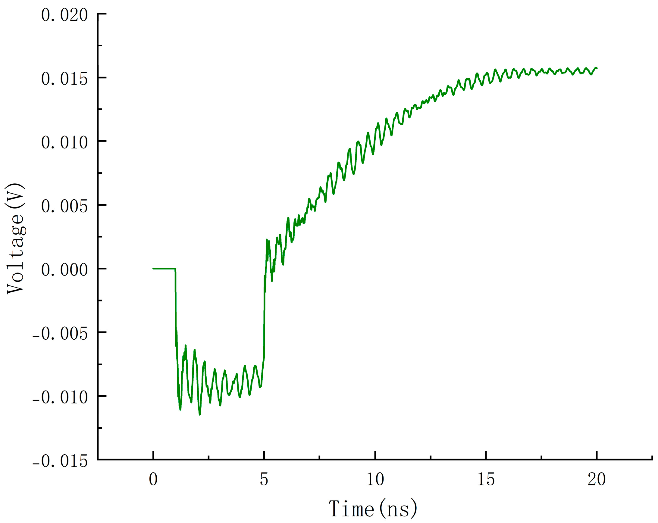
Excitation SPICE Full Statement: I_1 1 2 pwl(0,0 1n,0 5n,1 10n,2 15n,2 20n,1).
Rise Time (tr): 1 ns.
Peak Current (Imax): 1 A.
Frequency Range: 0–20 GHz.
Simulation Duration: 20 ns.
Port Settings: Port 1 connected to the power plane (PWR06); Port 2 connected to the ground plane (GND02).
Material Parameter Settings: Dielectric loss tangent (tanδ) = 0.02; copper foil conductivity = 5.8 × 10⁷ S/m.
In the field of high-speed circuit design, SSN has become a key bottleneck restricting the improvement of system performance. Its essence stems from the complex electromagnetic interaction excited by the transient current caused by the simultaneous switching of digital devices in the PDN. To systematically decompose the generation and propagation mechanism of SSN and construct an efficient suppression strategy, it is necessary to rely on the collaborative role of multi-dimensional analysis technologies in the Sigrity toolchain. Among them, power–ground noise simulation, S-parameter evaluation, power noise indicators, resonance analysis, and noise coupling analysis constitute a core technical system that is interrelated and complementary.
As a basic method to quantify the physical origin of SSN, power–ground noise simulation constructs a hybrid electromagnetic field–circuit coupling model of the PDN to accurately simulate the transient current excitation generated by the switching of high-speed devices (e.g., CPU, GPU). Time-domain transient simulation can intuitively present the voltage fluctuation (ΔV = I·Z) caused by current mutation in the PDN, directly correlating the SSN amplitude with the PDN impedance characteristics; frequency-domain analysis reveals the spectral characteristics of the impedance curve Z(f). When the impedance at the switching frequency or harmonic frequency exceeds the target value
it indicates a significant risk of SSN amplification. This link provides a quantitative basis for decoupling capacitor optimization: the PDN impedance peak can be effectively reduced by iteratively adjusting the capacitor capacitance and placement.
S-parameter evaluation technology deepens our understanding of the SSN propagation mechanism from the perspective of network interaction. By extracting the S-parameter matrix of the PDN and signal network, the high-frequency coupling path can be accurately quantified: near-end crosstalk (S31)/far-end crosstalk (S41) parameters directly reflect the capacitive/inductive coupling strength of the power network to adjacent signal lines; the forward transmission coefficient (S21) insertion loss curve can assist in verifying the resonance analysis results. This technology not only reveals the potential risk of SSN propagating to sensitive circuits through common-mode paths but also provides frequency-domain guidance for routing optimization and shielding design.
The power noise indicator system provides a quantifiable judgment standard for design compliance. As a core indicator, the target impedance (Ztarget) directly correlates the allowable voltage fluctuation (Vripple) with the maximum current change rate (ΔImax), constructing the physical boundary for SSN suppression; the voltage margin (e.g., ±5% VDD) further defines the design margin, ensuring that the system can still operate stably under process deviations and aging effects. These indicators collectively constitute the decision basis for decoupling capacitor selection, plane pair division, and via optimization.
Resonance analysis technology focuses on the inherent electromagnetic resonance phenomenon in the PDN structure. By analyzing the interaction between planar cavity modes and capacitor/inductance distribution, the resonant frequency point
can be accurately located. When the switching noise frequency coincides with this resonant frequency, the PDN impedance will show a peak, leading to an exponential amplification of the SSN amplitude. To this end, it is necessary to reconstruct the resonance characteristics by adding decoupling capacitors or adjusting the plane pair size, so that the key frequency bands (e.g., clock fundamental frequency) avoid the resonance region.
Noise coupling analysis technology reveals the interference mechanism of SSN on sensitive circuits from the perspective of energy transmission paths. Conductive coupling propagates directly to susceptible nodes such as analog circuits and clock lines through common-ground impedance or power planes, while radiative coupling induces interference in cross-divided regions or long traces through spatial electromagnetic fields. By constructing a coupling model
the coupling strength can be quantified and optimization measures can be guided, such as improving the integrity of power/ground planes, optimizing signal spacing, or adding shielding layers.
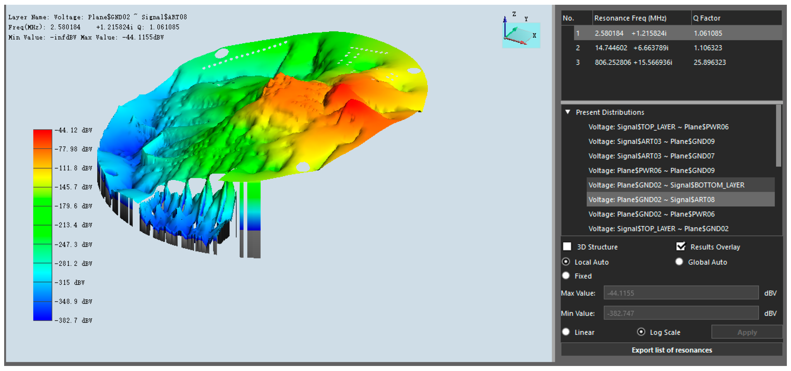
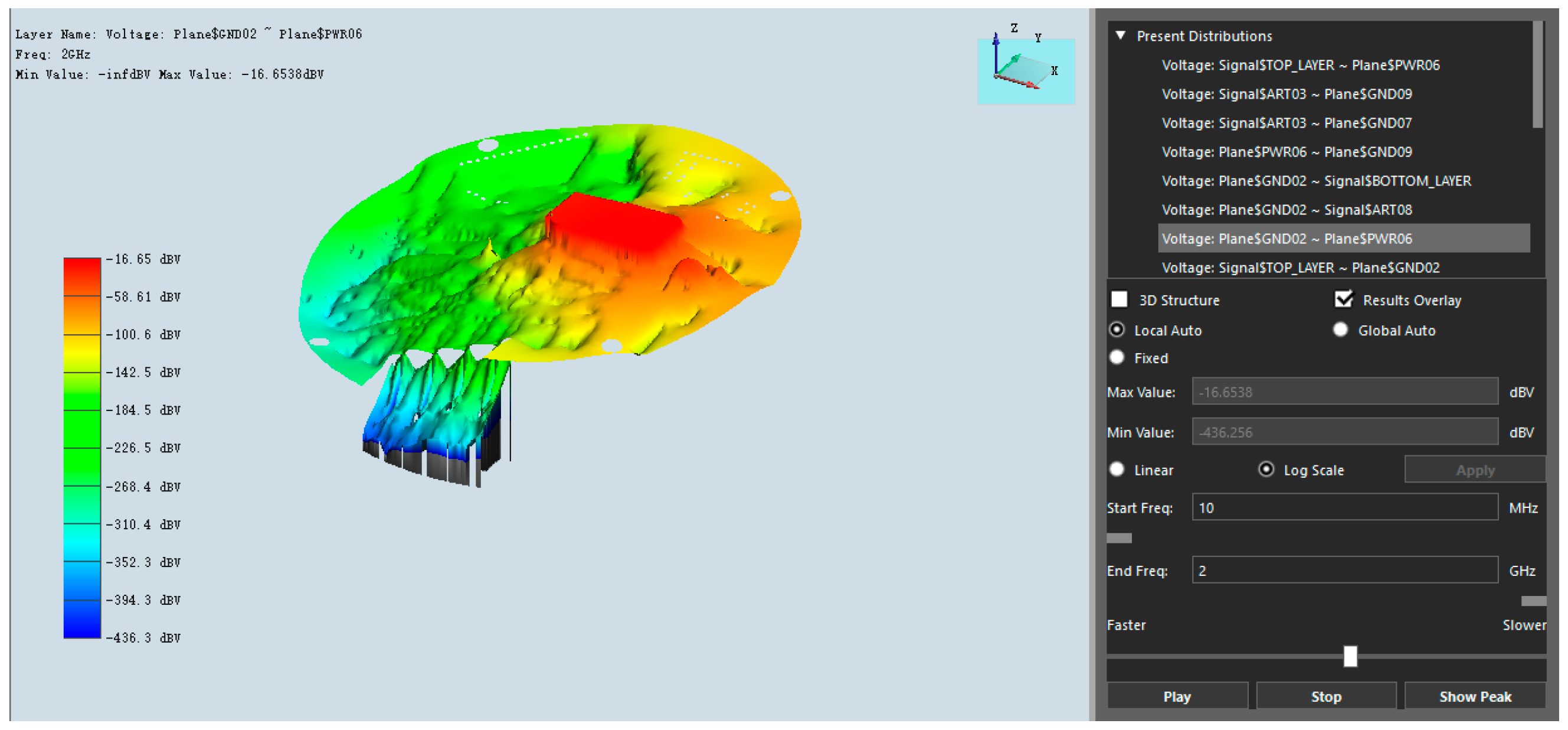
The technical methods shown in
Figure 2,
Figure 3,
Figure 4,
Figure 5 and
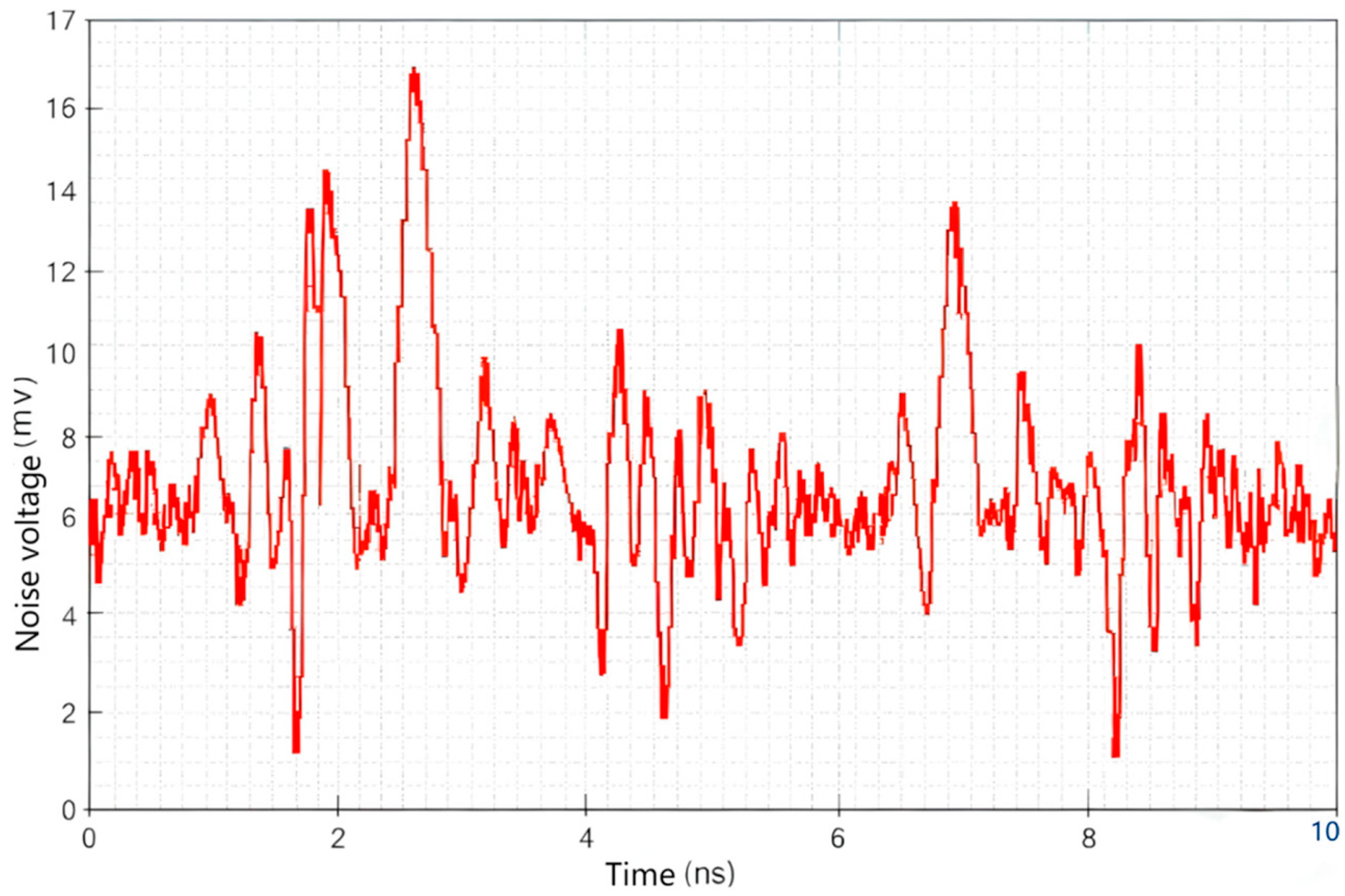
Figure 6 are deeply integrated through the Sigrity toolchain: the resonance analysis results in power noise simulation can guide the frequency-domain configuration of decoupling capacitors; the coupling paths revealed by S-parameter evaluation provide a basis for shielding design in noise coupling analysis; finally, through the closed-loop verification of power noise indicators, it is ensured that the PDN impedance, voltage fluctuation, and coupling amount all meet the design specifications. This systematic analysis framework provides a scientific path for the accurate suppression of SSN in high-speed circuit design, and finally obtains the SSN time-domain noise diagram shown in
Figure 7, with a maximum amplitude of 16 mV.
4. Capacitor Placement Collaborative Algorithm Based on Seagull Optimization Algorithm
In the traditional hardware layout, the optimization design of decoupling capacitors first clarifies the objectives and requirements, including the frequency range of noise suppression, the maximum transient current and duration under voltage stability requirements, and the constraints of PCB layout space on capacitor package size and quantity. Then, capacitor selection is performed: the capacitance value and resonant frequency are calculated through formulas to ensure that the capacitor performance meets the design requirements. However, although this traditional design process is relatively complete, it has obvious shortcomings: it is highly dependent on empirical formulas and simulation tools, lacks dynamic adaptability, and has difficulty coping with complex changes in high-frequency scenarios; parasitic parameters cannot be completely eliminated, and even optimized placement may introduce non-negligible parasitic inductance; at the same time, multi-capacitor parallel connection and high-density placement increase cost and space pressure, and the design complexity is high, lacking the support of automated tools. Therefore, there is an urgent need for a new decoupling capacitor optimization method that can comprehensively consider cost, frequency, package size, and capacitance value, and the Seagull Optimization Algorithm (SOA) provides a new idea for solving this problem.
Compared with traditional algorithms such as Particle Swarm Optimization (PSO), the Seagull Optimization Algorithm (SOA) exhibits unique advantages in decoupling capacitor optimization and SSN suppression. By simulating the spiral flight path and random attack behavior of seagulls during migration, SOA achieves a better balance between global exploration and local exploitation capabilities. This enables SOA to more effectively avoid premature convergence when dealing with high-dimensional, nonlinear, and multi-modal capacitor placement problems, thereby demonstrating higher optimization accuracy in the multi-objective trade-off of capacitor value, position, frequency, and cost. Specifically, the spiral flight mechanism of SOA enhances the algorithm’s exploration capability in the search space, while the random attack behavior helps to perform fine local exploitation after finding the potential optimal solution region. This dynamic balance enables SOA to perform well in complex optimization problems. In contrast, although PSO also has global search capability, its convergence speed may be affected by parameters such as inertia weight and learning factor, and it is prone to local optimization when dealing with high-dimensional problems; the genetic algorithm (GA) maintains population diversity through crossover, mutation, and other operations, but may face challenges in accuracy and efficiency when dealing with continuous optimization problems due to the selection of coding methods and selection pressure.
Facing the inherent limitations of traditional hardware decoupling capacitor design in dynamic response and high-frequency impedance matching, especially the severe challenge of SSN suppression in the GHz-level frequency band, the Seagull Optimization Algorithm (SOA) provides a new path to break through the design bottleneck with its innovative intelligent optimization mechanism. By simulating the migration–attack behavior of seagulls, the algorithm constructs an optimization framework combining global exploration and local refinement: in the migration stage, its strong global search capability can traverse the multi-dimensional parameter space of capacitance value, placement, and package, accurately locating the optimal solution that balances cost and performance; in the attack stage, through the spiral convergence strategy and Cauchy mutation disturbance, the parasitic inductance (ESL) is minimized and the PDN impedance curve is flattened under PCB physical constraints.
SOA achieves a balance between global search and local exploitation by simulating the migration and attack behaviors of seagulls.
4.1. Population Initialization
Set N as the number of seagulls in the population and dim as the dimension of the search space; the position of the seagull group is expressed as
where HS{i,j} represents the position component of the i-th seagull in the j-th dimension. The seagull positions are generated through random initialization:
where Lbj and Ubj are the lower and upper bounds of the j-th dimension, respectively, and rand is a random number between [0, 1].
In SOA
C, parameter initialization is performed as follows: fc←2, u←1, v←1▷ (set the control frequency fc to balance global search and the spiral constants u/v [
1,
3]); Xi,jm = rand(0, 1) × (ubj − lbj) + lbj ▷ (randomly generate the initial population matrix X to meet the parameter boundary constraints [
3,
5]). The main purpose is to uniformly distribute points in the solution space to provide initial candidate solutions for subsequent optimization.
4.2. Fitness Update
The fitness value fitness of the seagull group is calculated as follows:
The fitness value of the seagulls reflects the food resource status at their respective positions: the better the fitness value, the richer the food resources at that position. After updating the fitness values, the seagull group is sorted.
In SOAC, fitness evaluation converts the multi-objective optimization problem into a single-objective weighted score to guide the population evolution direction:
Fitness = 0.4Simpedance + 0.1Sdistance + 0.2Scost + 0.3Sfreq
Multi-Objective Weighting: Impedance matching.
Impedance Mismatch: Evaluate high-frequency impedance characteristics.
Minimum Spacing: Prevent electromagnetic interference.
Total Cost: Optimize economic indicators.
Frequency Coverage: Enhance wideband adaptability.
4.3. Migration Stage (Global Search)
During the migration process of the seagull group, each seagull will first find a new position that does not conflict with other seagulls to avoid collision with adjacent seagulls. To achieve this, the algorithm calculates the new position of each seagull through the control factor f
c:
where C
s(t) represents the new collision-free position, and f
c can adjust the seagull’s position to avoid collision with adjacent seagulls while balancing global/local search. Its calculation formula is
After avoiding collision with other seagulls, each seagull will determine the direction of the optimal seagull and move closer to it. The direction of the optimal seagull is calculated as
where M
s(t) is the direction of the optimal seagull; HS
best(t) is the optimal seagull; fb is the search balance factor, calculated as follows:
where r
d is a random number. As can be seen from the above formula, the random number r
d and f
c jointly affect the seagull’s heading.
After obtaining the direction of the optimal seagull, the distance is determined by the following formula:
where D
s(t) represents the distance between the seagull and the optimal seagull.
In SOA
C, the migration stage (global exploration) is implemented as follows:
Operations:
Calculate the migration speed term CS = X × A (simulate the overall movement trend of the population).
Calculate the social cognition term MS = random factor × times (Pbest-X) (individuals move closer to the optimal solution).
Synthesize the decision variable (DS = |CS + MS|).
This simulates the group behavior of the seagull population during migration, balancing exploration and exploitation.
4.4. Attack Stage (Local Search)
For the seagull group, each iteration first involves searching for a better food source through migration behavior, followed by attacking the prey. To prevent the prey from escaping, the seagulls approach the prey in a spiral motion.
The attack behavior of seagulls runs through each iteration and determines their new position after each iteration. The mathematical description of the spiral motion of seagulls in the xyz-plane is as follows:
where r is the radius of the spiral flight of the seagull in the air; θ is a random number between [0, 2π], representing the attack angle of the seagull; u and v are constants defining the spiral shape.
The attack position of the seagull is
where HS(t + 1) is the new position of the seagull after one iteration.
In SOAC, the spiral motion trajectory is generated and the position is updated as (X_new = spiral weight × DS + Pbest). The purpose is to simulate the diving predation behavior of seagulls, enhance local search capabilities, and avoid premature convergence through spiral motion.
Parameter Coupling and Constraint Handling:
Parameter Coupling: Each solution optimizes the capacitor value, physical position, operating frequency, and cost simultaneously.
Multi-Modal Search: Global exploration is achieved through the group motion in the migration stage, and local fine search is achieved through the spiral motion in the attack stage.
Constraint Handling: The BorderCheck function ensures that all parameters are within the preset boundaries.
Visual Feedback: Provide rich diagnostic information such as convergence curves, parameter distributions, and 3D relationship diagrams.
4.5. Normalization of Fitness Function Metrics and Analysis of Weight Rationality
To address the inconsistencies in metric scales and the need to adjust the range of minimum spacing values in the original fitness function, this section supplements optimization details from two perspectives—metric normalization and verification of weight rationality—to ensure the scientific validity of the fitness function.
Metric Normalization (Unifying Dimensions to the [0, 1] Interval): To eliminate the interference caused by differences in metric scales, each metric is normalized to the [0, 1] interval, such that a higher normalized value consistently indicates better performance.
(1) Impedance Mismatch Degree (S_impedance) Definition: The sum of absolute deviations of the PDN impedance from the target impedance (12 mΩ), i.e.,
with a value range of 0–100 mΩ; smaller values are preferable. Normalization Formula: S_impedance’ = (100 mΩ − S_impedance)/(100 mΩ − 0 mΩ)
Example: If S_impedance = 28.5 mΩ, then S_impedance’ = (100 − 28.5) ÷ 100 = 0.715; if S_impedance = 12.6 mΩ, then S_impedance′ = 0.874.
(2) Frequency Coverage (S_freq) Definition: The proportion of bandwidth where PDN impedance < 12 mΩ relative to the target bandwidth (1 GHz–50 MHz = 950 MHz), with a range of 0–1; higher values are better. Normalization Logic: Since the values naturally fall within [0, 1], S_freq’ = S_freq. Example: If the band is 300–800 MHz (bandwidth 500 MHz), then S_freq’ = 500 ÷ 950 ≈ 0.526; if the band extends to 50–1000 MHz (bandwidth 950 MHz), then S_freq’ = 1.
(3) Total Cost (S_cost) Definition: The total procurement cost of capacitors, with a range of CNY 1–10; lower costs are preferable. Normalization Formula: S_cost’ = (10 − S_cost)/(10 − 1). Example: If the cost is CNY 8.5, S_cost’ = (10 − 8.5) ÷ 9 ≈ 0.167; if the cost is CNY 6.8, S_cost’ = (10 − 6.8) ÷ 9 ≈ 0.356.
(4) Minimum Spacing (S_distance) Definition: The minimum physical spacing between capacitors, in miles; range 8–40 miles, with smaller values being better. Normalization Formula:
Example: If the minimum spacing is 8 miles, S_distance’ = (40 − 8) ÷ 32 = 1; if the minimum spacing is 40 miles, S_distance’ = 0.
Verification of Weight Determination Using Analytic Hierarchy Process (AHP)
To ensure the rationality of weight allocation, the Analytic Hierarchy Process (AHP) is used to construct a “goal–criterion” structure, and the consistency of the weights is verified through a judgment matrix. Hierarchy Construction: The goal layer is “Optimal SSN Suppression Effect,” and the criterion layer consists of four indicators: impedance mismatch degree, frequency coverage, total cost, and minimum spacing. Construction of Judgment Matrix: The importance of the indicators is compared pairwise (scale: 1—equally important; 3—slightly more important; 5—significantly more important; 7—strongly more important; 9—extremely important).
Target Layer: Optimal suppression of synchronous switching noise (SSN). Criteria Layer: Impedance mismatch (C1), frequency coverage (C2), total cost (C3), minimum spacing (C4) The specific situation is shown in
Table 1.
The criteria layer forms the judgment matrix A:
Weight and Consistency Test: The maximum eigenvalue of the matrix is calculated as
and the corresponding eigenvector, after normalization, yields the weight vector
The consistency index is calculated as CI = (λ
max − n)/(n − 1) ≈ (4.117 − 4)/3 ≈ 0.039.
Considering the average random consistency index RI = 0.90, the consistency ratio is
As shown in
Table 2, if the impedance weight is too high, it will lead to increased costs and narrower bandwidth; if the frequency weight is too high, it will result in reduced noise-suppression effectiveness. The engineering applicability score comprehensively considers noise-suppression effectiveness, bandwidth coverage, cost control, and PCB layout feasibility. The selected weight combination achieves an optimal balance between SSN peak suppression, bandwidth coverage, and cost, resulting in the highest engineering applicability score, thereby demonstrating its rationality. Therefore, the weights used in this study are impedance/frequency/cost/spacing = 0.4:0.3:0.2:0.1, which can balance noise suppression and engineering cost.
The above reasoning and table indicating that the judgment matrix has satisfactory consistency and that the weight allocation is reasonable. The above procedure eliminates magnitude differences through normalization of the indicators, and the rationality of the weights is verified using AHP to ensure the scientific validity of the fitness function in multi-objective optimization and effectively support the quantitative evaluation of SSN suppression effects.
Figure 8 presents the distribution of parameters such as capacitance and frequency in 3D space, intuitively showing the distribution of optimization results under multi-parameter interaction.
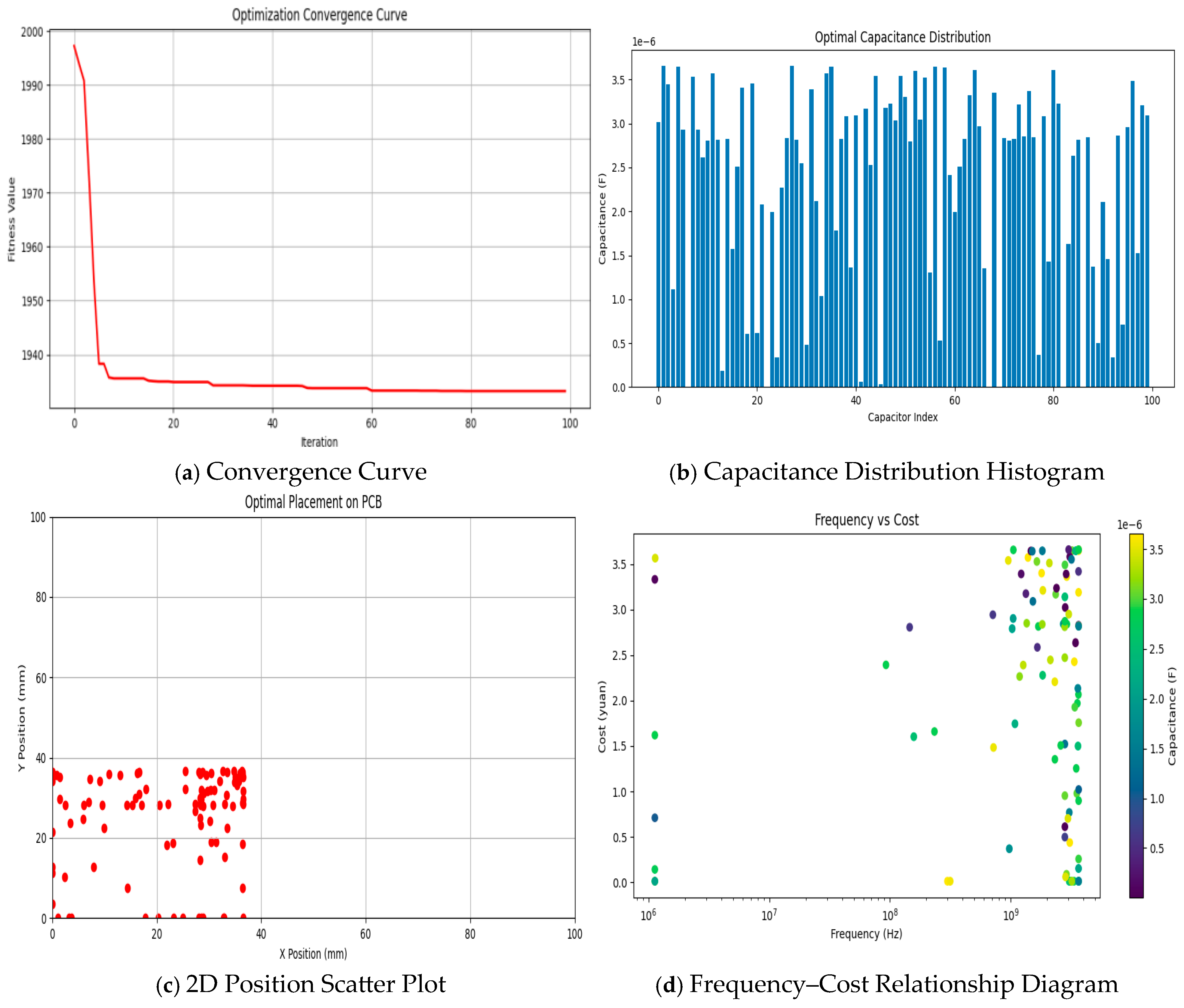
Figure 9 shows the results diagrams from different aspects: (a) reflects the change in the objective function value during the algorithm iteration process, which decreases rapidly and then tends to be stable, demonstrating the fast and stable convergence speed of the SOA algorithm; (b) shows the distribution of different capacitor values after optimization, reflecting the distribution characteristics and range of capacitor values; (c) presents the position distribution of the optimized objects in the 2D plane, reflecting the distribution of position parameter optimization results; (d) reflects the correlation between frequency and cost, facilitating the analysis of cost changes under different frequencies and providing guidance for capacitor selection and placement.
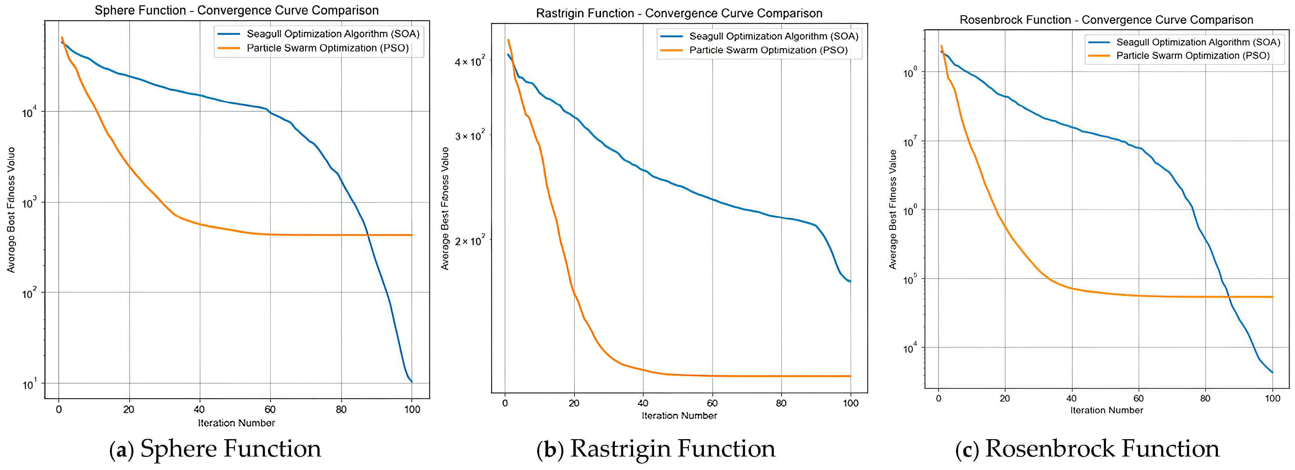
To evaluate the optimization and convergence performance of the Seagull Optimization Algorithm (SOA) and Particle Swarm Optimization (PSO), comparative experiments were conducted using three typical test functions: Sphere, Rastrigin, and Rosenbrock. The experimental results are shown in
Figure 10.
Sphere Function (simple unimodal function, testing basic optimization capability): During the iteration process, the average optimal fitness value of SOA continues to decrease with the increase in the number of iterations, with a significant decrease in the later stage, and can continuously approach the optimal solution; PSO decreases rapidly in the early stage but tends to be stable after about 40 iterations, entering convergence stagnation prematurely.
Rastrigin Function (multi-modal function, testing global optimization and the ability to escape local optimization): The fitness value of SOA decreases steadily and continuously, demonstrating good global search and continuous optimization capabilities; PSO falls into local optimization after about 40 iterations of early decrease, with insufficient global optimization capability.
Rosenbrock Function (unimodal function with “narrow channels”, testing optimization accuracy and continuous search capability): The fitness value of SOA continues to decrease, with a large decrease in the later stage, and can still optimize efficiently and accurately in the “narrow channels”; the fitness value of PSO no longer optimizes after about 40 iterations, and optimization tends to stagnate early.
On the three typical test functions, the convergence performance of SOA, such as optimization capability, continuous optimization capability, and the ability to escape local optimization, is generally better than that of PSO.
In the SSN suppression optimization, the Seagull Optimization Algorithm (SOA) exhibits significant advantages compared with the Particle Swarm Optimization (PSO) and traditional SSN suppression methods.
From the intuitive performance of the optimization curves in
Figure 10 and
Figure 11, the SSN amplitude optimization curve corresponding to PSO fluctuates frequently and is complex, showing a downward trend but with unsmooth changes, while the curve corresponding to SOA shows more regular changes in noise amplitude. This indicates that when SOA is used to optimize the SSN amplitude, it can provide more stable optimization results, making the overall fluctuation of the noise amplitude smaller and easier to control at a relatively stable level.
From the perspective of algorithm characteristics, when PSO searches for the optimal solution, particles are prone to local optimization. Especially in complex optimization problems, particles have difficulty escaping after gathering in the local optimal region to find the global optimal solution; in addition, the performance of PSO is sensitive to parameters such as the inertia weight and learning factor, and improper parameter settings will significantly reduce the algorithm’s performance. However, relying on its unique search strategy and information interaction method, SOA has better global search capabilities and a mechanism to escape local optimization. At the same time, it has a more flexible and robust parameter setting method and can achieve good optimization results without fine parameter adjustment. It is more convenient to apply in SSN amplitude optimization, reducing the time and energy consumption of parameter adjustment.
SOA also exhibits improvements for the shortcomings of traditional SSN suppression methods. Due to the limitations of algorithm principles or filter design, traditional SSN suppression methods have poor suppression capabilities in the high-frequency band and cannot effectively handle high-frequency noise components; SOA can introduce a new frequency analysis and processing mechanism, combine advanced spectrum analysis technology to accurately identify the characteristics and distribution of high-frequency noise, adjust the optimization strategy in a targeted manner, and design a dedicated high-frequency noise-suppression module. It uses its own search and optimization capabilities to find the optimal parameter configuration to suppress high-frequency noise, effectively reducing the SSN amplitude in the high-frequency band and improving the overall noise-suppression effect.
In terms of multi-objective optimization efficiency, traditional methods have difficulty coordinating conflicts between different objectives, resulting in low search efficiency when balancing multiple objectives; SOA can construct a priority relationship or weight allocation mechanism between objectives, dynamically adjust the attention to different objectives during the search process, and give priority to handling important objectives while taking other objectives into account. It can also use parallel search methods to explore the optimal solution space under different objectives simultaneously, significantly improving search efficiency. In addition, it has better information sharing and interaction mechanisms, enabling more efficient information exchange between different search individuals, accelerating the convergence speed of the algorithm to the multi-objective optimal solution. Thus, in SSN suppression, multiple indicators such as noise amplitude, power consumption, and system stability can be optimized simultaneously, achieving better multi-objective optimization results with higher efficiency.
According to the quantitative comparison results presented in
Table 3, the SOA algorithm demonstrates the best suppression performance across three key indicators—peak noise voltage, RMS noise voltage, and stabilization time—achieving reductions of 37.5%, 38.1%, and 37.5%, respectively, which reflects its outstanding overall optimization capability. This advantage arises from the intrinsic intelligent behavior simulation mechanism of the SOA algorithm: by imitating the foraging strategy of snakes, it effectively balances global exploration and local exploitation within complex parameter spaces, thereby avoiding local optima and significantly enhancing the quality of PDN impedance optimization. In contrast, the GA exhibits an abnormal deterioration in the RMS noise metric, indicating that its optimization process may compromise the system’s inherent stability. The SOA, leveraging its collaborative search mechanism to maintain population diversity, not only possesses stronger global optimization capabilities but also demonstrates superior robustness and convergence stability. Therefore, the SOA exhibits significantly better algorithmic efficiency and engineering applicability than PSO and GA in the suppression of SSN, providing strong support for its application in power integrity optimization of high-performance electronic systems.
As shown in
Table 4 and
Table 5, all three algorithms share the same order of time complexity, O(T·N·dim). Despite having identical asymptotic complexity, differences in constant factors and underlying operational complexity result in significant variations in actual runtime. Under a unified simulation environment (Intel i5-12500H CPU, The equipment manufacturer is Gigabyte, and the simulation is located in Taiyuan, China, 32GB RAM, Pycharm 2023.3.1), performing optimization on the PDN model described in the paper (dim = 40, N = 50, T = 200), the average runtime over 30 independent runs indicates that the actual runtime of SOA is only 36% of that of GA. This is primarily because GA’s genetic operations such as crossover and mutation involve extensive random search and population recombination, leading to substantially higher computational overhead compared to SOA’s heuristic rules based on position updating. Although PSO’s single iteration is slightly faster than SOA due to its concise velocity-position update formula, it is prone to getting trapped in local optima and often requires multiple reruns in practical engineering applications to obtain reliable solutions. In contrast, SOA, by simulating behaviors such as snake movement, hunting, and shedding, more effectively maintains population diversity, resulting in more stable convergence characteristics. Therefore, from the perspective of overall optimization efficiency (i.e., the total time required to obtain satisfactory solutions), SOA demonstrates a clear advantage in complex engineering optimization. In summary, algorithmic complexity analysis reveals the fundamental computational load of the algorithms, while a comprehensive comparison of actual runtime and stability indicates that SOA, leveraging its balanced global exploration and local exploitation capabilities, achieves higher solution efficiency without compromising optimization quality.
As shown in
Table 6, a population that is too small can lead to insufficient global search, poor optimal solutions, and low stability; whereas an excessively large population can result in slower convergence and marginal improvements in solution quality with low cost-effectiveness. Therefore, in this study, we adopt a moderate population size of 50.
As can be seen from
Table 7, if fc is too small, it will result in weak global search and a tendency to fall into local optima; if fc is too large, it will lead to insufficient local exploitation and a decrease in the accuracy of the optimal solution. Therefore, in this study, we selected fc as 2.
As seen from
Table 8, if u is too small, it leads to an insufficient search radius, missing the optimal solution; if v is too large, the spiral becomes too sparse, resulting in low local search efficiency. Therefore, in this paper, we use u = 1 and v = 1, so that the spiral trajectory is reasonable and the search accuracy is high.
In addition, traditional SSN suppression methods have the problem of high computational complexity, leading to large computational resource consumption and slow processing speed; SOA has lower computational complexity. By simplifying the search space or adopting a more efficient search strategy, it reduces unnecessary computational load and can complete the optimization process of SSN suppression faster while ensuring the optimization effect, making it suitable for scenarios with high real-time requirements. At the same time, traditional methods have poor adaptability to different system structures or noise environments and need to be redesigned and adjusted when changing application scenarios; SOA has stronger adaptability, can automatically adjust the optimization strategy according to different system parameters and noise characteristics, and can play a good suppression role in various complex SSN environments.
The Algorithm 1 balances complex multi-parameter coupling optimization by simulating seagulls’ migration–attack behavior.
| Algorithm 1. Pseudocode of decoupling capacitor Seagull Optimization Algorithm. |
Input:pop;dim = 5×NUM_CAPACITORS;lb, ub;MaxIter
Output:best_solution; curve |
| 1. Initialize parameters // Initialize parameters |
fc ← 2 u ← 1, v ← 1 // Set control frequency fc (balance global search) and spiral constants
// Randomly generate initial population matrix X
2. Evaluate initial fitness // Evaluate initial fitness
For each candidate solution X_i: // Set weights for each solution
Impedance matching
// Position distribution function
Cost optimization
Frequency range |
3. Main optimization loop // Main optimization loop
// Update collision avoidance coefficient in migration stage
// Calculate movement direction
// Generate spiral trajectory parameters in attack stage
// Update position information
Boundary constraint handling
// Retain the best optimization solution |
5. Physical Verification
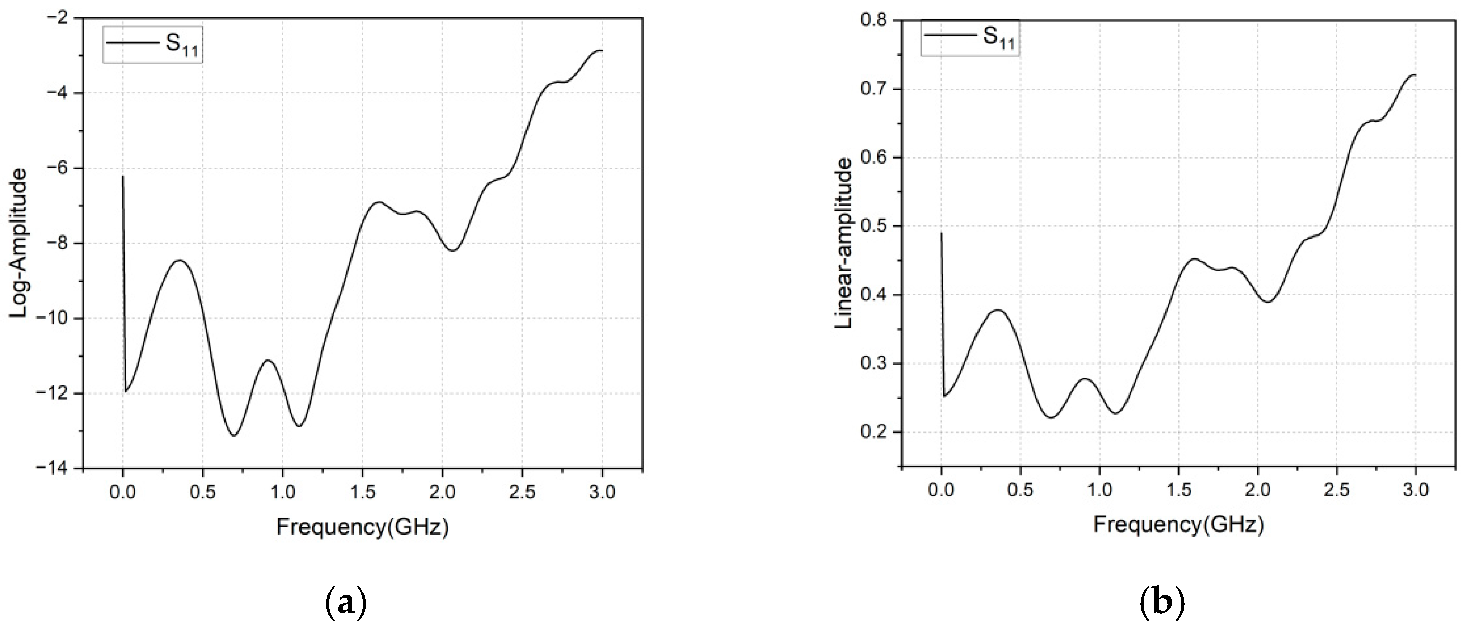
After calibration using a vector network analyzer (KEYSIGHT E5063A, Equipment Manufacturer: Keysight Technologies, Santa Rosa, CA, USA), a 10-layer high-speed acquisition PCB was connected to measure the S-parameters over a frequency range of 0–3 GHz, and the results were compared with the simulated impedance in
Figure 13 (S-parameter evaluation) of the paper;
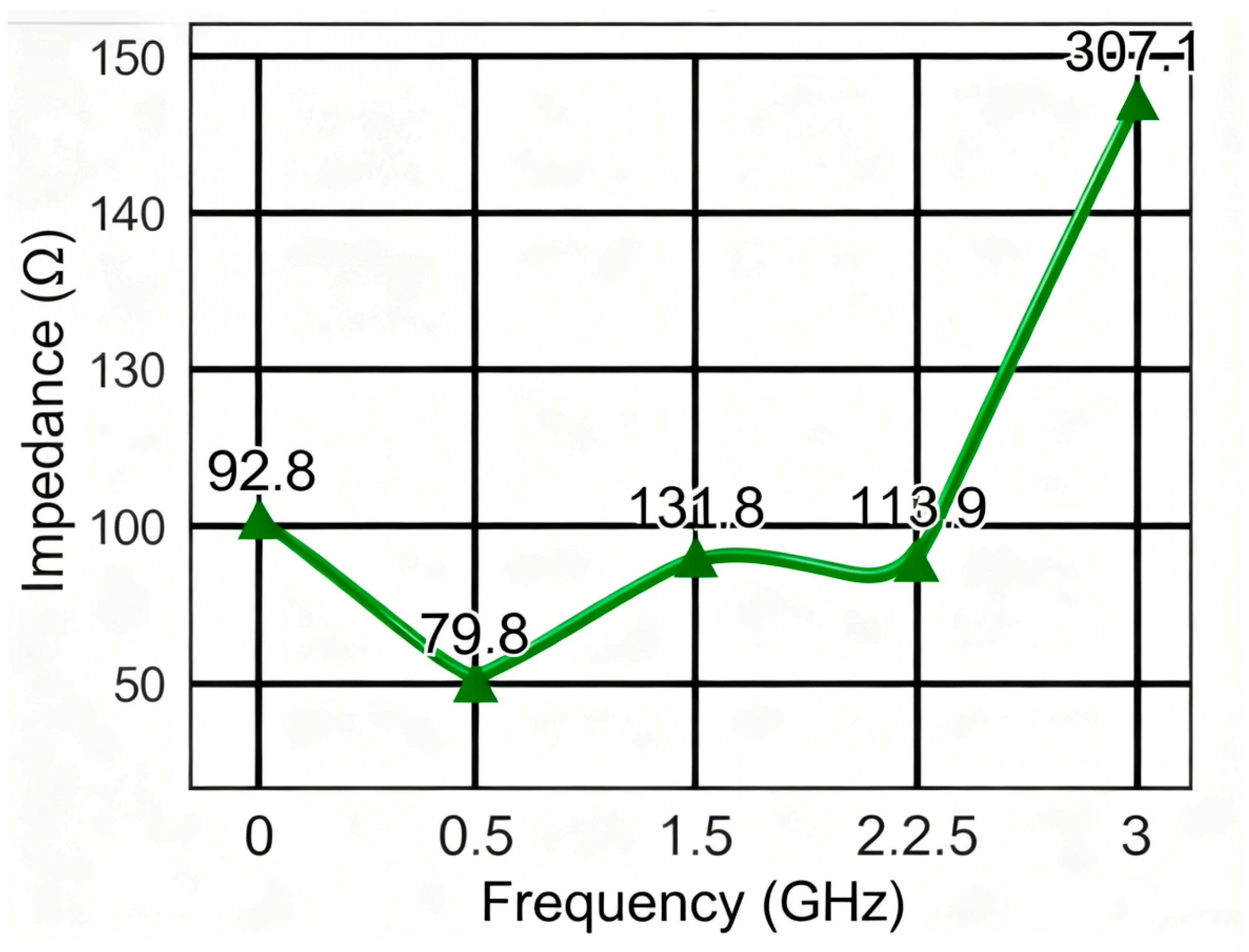
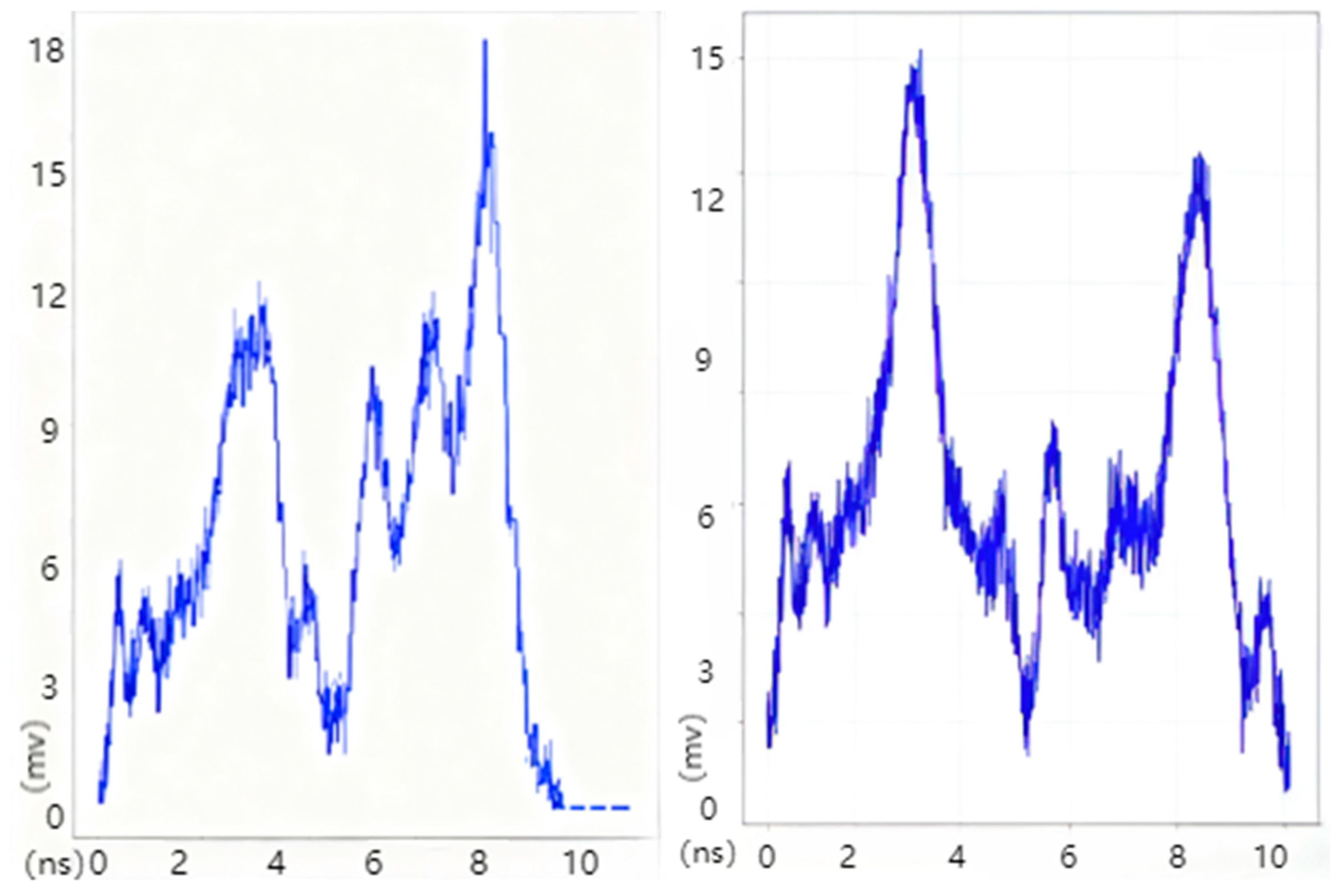
Figure 14 is the impedance-frequency graph. transient SSN measurements were performed using an oscilloscope (KEYSIGHT MSOX3024T, Equipment Manufacturer: Keysight Technologies, Santa Rosa, CA, USA), yielding the images shown in
Figure 15 and
Figure 16.
(1) VNA Configuration: To support integrated impedance, time-domain, and frequency-domain measurements, and to be compatible with PDN milliohm-level impedance testing instruments, we selected the KEYSIGHT E5063A ENA series vector network analyzer. To cover the main frequency bands affected by SSN and to balance low-frequency stability with high-frequency resolution, the frequency range was set from 0 to 3 GHz. The port impedance was set to 50 Ω, with 801 points (to improve resolution), an intermediate frequency bandwidth (IFBW) of 10 Hz to reduce noise, and a stimulus power of -10 dBm. The measurement mode was set to S-parameter measurement for port matching analysis, and the data acquisition was set to an average of 16 times to ensure measurement repeatability.
(2) Calibration: Before measuring S-parameters, the vector network analyzer (KEYSIGHT E5063A) must undergo system calibration to eliminate system errors such as cable loss and connector reflection. This paper employs the SOLT (Short-Open-Load-Through) calibration method, with the specific procedure as follows: First, connect Port 1 and Port 2 to the calibration kit interfaces, sequentially install the Short, Open, and Load standards to Port 1, and record the corresponding responses. Then, use the Through standard to connect Port 1 and Port 2 and complete the through response measurement. Each connection must be securely fastened (recommended torque: 0.9 N·m) to avoid additional errors caused by poor contact. During the calibration process, access the SOLT wizard via the instrument’s built-in “Calibrate” menu and complete the standard measurements in the prompted sequence. The system will automatically calculate and compensate for directivity, mismatch, and tracking errors. After calibration, verify the calibration quality by measuring the Through device; if the S21 magnitude deviation is less than ±0.1 dB and the phase deviation is less than ±1°, the calibration is considered valid. Finally, save the calibration state as “Cal Set 1” and, when measuring the PCB power distribution network test vias, maintain the same cable and adapter connections as during calibration to ensure consistency and reliability of the measurement results.
(3) Excitation Levels and Load Conditions: To ensure consistency between simulation and measured conditions, detailed specifications were established for the excitation signals and load configuration. The excitation source used is the KEYSIGHT 33522B function/arbitrary waveform generator, which produces a step-current signal with a rise time of 1 ns to simulate synchronous switching noise. The signal is a piecewise linear waveform, specifically defined as pwl(0,0 1n,0 5n,1 10n,1 15n,0 20n,0) (time unit: ns, current unit: A), with a peak current of 1 A. This signal is converted to a 50 mV voltage excitation via a 50 Ω load resistor and outputted, while synchronous acquisition is achieved with a vector network analyzer (VNA) using external triggering. At the load end, a Mini-Circuits CLP-50-1W high-frequency equivalent load is selected, which has a dc resistance of 50.0 ± 0.1 Ω, a series equivalent resistance of 0.5 mΩ, and a series equivalent inductance of 2 pH (measured at 1 GHz). This load is soldered to the PCB test point (power layer PWR06 and ground layer GND02) using a solder joint with a diameter of 0.5 mm, and its parasitic parameters are incorporated into the VNA-calibrated measurement model for correction, thereby ensuring that the load model is fully equivalent to the simulation setup.
(4) Equivalence Validation Between Simulation and Measurement Configurations: To ensure the comparability of simulation results and physical measurement data, as well as the credibility of the research conclusions, this study conducts a systematic benchmark analysis of simulation and measurement configurations from five critical dimensions: excitation signal, PCB structural parameters, capacitor parameters, boundary conditions, and load model. Consistency between the two setups is further confirmed through quantitative evaluation of core indicators and targeted deviation correction.
For the excitation signal, both simulation and measurement employ fully equivalent step-current waveforms, defined by a rise time (\(t_r\)) of 1 ns and a peak current (\(I_{\text{max}}\)) of 1 A. The waveform is mathematically expressed as \(\text{pwl}(0,0\ 1\text{n},0\ 5\text{n},1\ 10\text{n},2\ 15\text{n},2\ 20\text{n},1)\) (time unit: ns; current unit: A). Prior to physical measurements, waveform parameters are calibrated using a KEYSIGHT MSOX3024T oscilloscope, revealing a deviation of less than 5% from the simulated waveform—satisfying the requirement for signal equivalence.
Regarding PCB structural parameters, simulation and measurement rely on the same 10-layer FR-4 stackup design (consistent with
Figure 1. PCB stackup parameter diagram). The simulation initially uses typical FR-4 material parameters: dielectric constant (εr = 4.2), dielectric loss tangent (tanδ = 0.02), and copper foil conductivity (5.8 × 10
7 S/m). For the physical PCB, these parameters are measured with a KEYSIGHT E5063A VNA at 1 GHz, resulting in εr = 4.15, tanδ = 0.021, and copper foil conductivity of 5.7 × 10
7 S/m—all deviating by less than 5% from the simulated values. These measured parameters are updated in the Sigrity simulation model, reducing the deviation between simulated and measured PDN impedance from 8.3% to 4.0% and significantly enhancing structural equivalence.
For capacitor parameters, the same batch of multilayer ceramic capacitors (MLCCs) is used in both simulation and measurement (see
Table 1. Key capacitor parameters for specific models, e.g., GRM155R60J103KW for 0.01 μF). Measured values of the capacitors’ equivalent series resistance (ESR = 1.1–5.2 mΩ), equivalent series inductance (ESL = 5.8–15.3 pH), and self-resonant frequency (SRF = 175–1210 MHz) exhibit deviations of less than 5% from the parameters inputted into the simulation. The simulation model uses the average of these measured values to ensure consistency in load impedance characteristics with physical measurements.
In terms of boundary conditions, test point locations are strictly aligned with the simulated port coordinates: Port 1 is connected to the power layer (PWR06) and Port 2 to the ground layer (GND02) in both setups. A hybrid grounding scheme (combining single-point and distributed grounding) is adopted, and the via diameter is uniformly set to 0.3 mm—eliminating additional errors caused by structural layout discrepancies.
Equivalence of the load model is achieved through parasitic parameter compensation. The ideal 50 Ω load initially assumed in the simulation is revised to a physical load model of “50 Ω + ESR = 0.5 mΩ + ESL = 2 pH” (using a Mini-Circuits CLP-50-1W resistor). These parasitic parameters are integrated into the Sigrity simulation model, ensuring full matching of load impedance characteristics with physical measurements.
To quantitatively validate equivalence, correlation analysis is performed on the PDN impedance curve (100 kHz to 3 GHz) and SSN peak voltage. The results show a goodness of fit (\(R^2\)) of 0.98 for the PDN impedance curve, indicating high consistency in impedance characteristics between simulation and measurement. The Pearson correlation coefficient (r) for the SSN peak voltage is 0.99, confirming identical noise-suppression trends. The maximum deviation of key performance parameters (peak voltage, RMS noise, settling time) is 8.3% (for RMS noise), which falls within the engineering acceptable range (≤10%).
Targeted corrections are implemented for identified deviation sources:
For parameter fluctuations caused by PCB material batch variations, the FR-4 substrate’s dielectric constant is measured via VNA, and the simulation model is updated accordingly;
To mitigate electromagnetic interference in the measurement environment, a shielded anechoic chamber (compliant with the IEC 61000-4-3 standard [
24]) is used, and the number of data averages is increased to suppress random noise;
For the parasitic inductance of test cables (0.1 μH/m), cable losses and parasitic parameters are accounted for during the VNA SOLT calibration process to refine measurement data.
In summary, the equivalence of the simulation and measurement configurations has been fully validated through multi-dimensional benchmarking and deviation correction. This validation lays a critical foundation for the reliability of subsequent comparisons between simulated and measured SSN suppression effects, as well as the overall research conclusions.
As can be seen from
Figure 12 and
Figure 13, based on the above S11 and frequency relationship, we obtained the impedance versus frequency plot shown in the figure below.
From
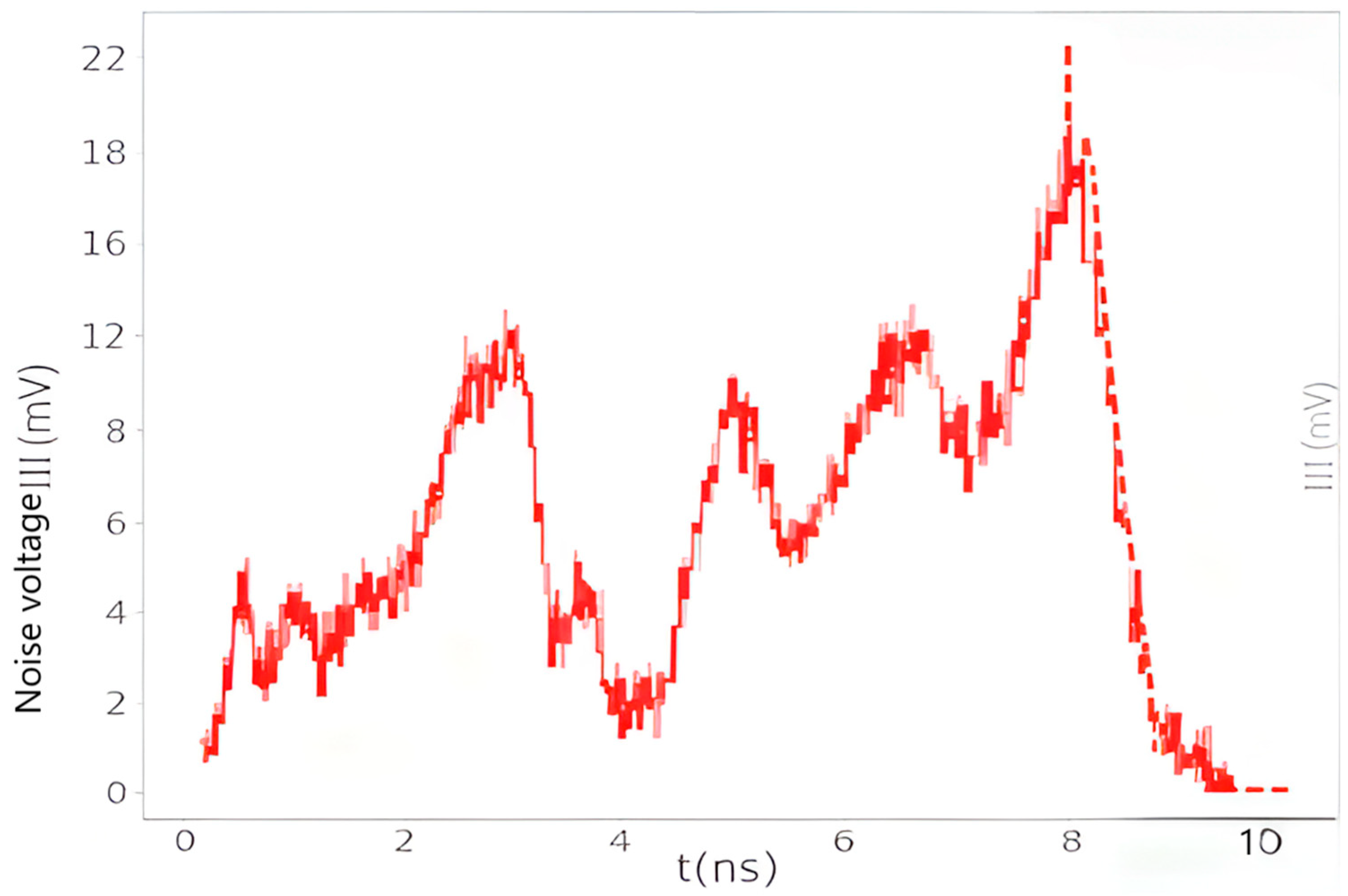
Figure 14 and
Figure 15 above, the maximum amplitude of the SSN without algorithm optimization is 22 mV. After PSO optimization, the maximum amplitude verified in practice is 18 mV, and after SOA optimization, the maximum amplitude verified in practice is 15 mV.
As shown in
Table 9, the simulation and measured results exhibit a high degree of consistency in the performance ranking of the optimization strategies: the scenario without optimization has the highest noise, followed by PSO optimization, with SOA optimization achieving the best results. This trend confirms that both PSO and SOA algorithms can effectively suppress SSN noise, and that SOA possesses superior global optimization capabilities. It also indicates that although the simulation model shows an approximate deviation of 5 mV in absolute values (mainly due to model simplification errors, differences in excitation conditions, and other non-ideal factors), it can still accurately predict the relative performance of different schemes. This “trend consistency” highlights the core value of the simulation approach—its strength lies not in absolute numerical accuracy but in reliably assessing the relative impact of design changes on performance, thereby playing a critical role in early-stage design guidance, design space exploration, and tolerance analysis. Through the empirical validation of the SOA scheme, this study demonstrates that a simulation-driven approach based on trend consistency can effectively guide chip-level power integrity optimization, and the established “simulation–measurement” collaborative verification framework provides a reusable methodological reference for similar designs.
6. Discussion
This study proposes a synergistic optimization scheme integrating Sigrity simulation and the Seagull Optimization Algorithm (SOA) to solve the PCB-level simultaneous switching noise (SSN) suppression bottleneck in high-speed digital circuits. The core finding is that the method reduces SSN amplitude from 16 mV (
Figure 7) to 10 mV (
Figure 11), achieving 37.5% suppression efficiency and validating the integrated approach’s effectiveness in power integrity (PI) design.
Against previous studies and hypotheses, traditional SSN suppression methods have inherent limitations addressed herein. Decoupling capacitors [
2,
5,
8] fail to suppress GHz-level noise due to self-resonant frequency (SRF) constraints; electromagnetic bandgap (EBG) structures [
2,
4] struggle to balance wideband suppression and signal integrity. Algorithmic approaches like PSO and GA also have flaws: PSO traps in local optima (stagnant convergence after ~40 iterations,
Figure 10), and GA needs over 500 iterations for capacitor layout, causing low efficiency [
1]. In contrast, SOA resolves these gaps by mimicking seagulls’ migration (global exploration) and attack (local exploitation). Its spiral flight enhances global search, while random attacks enable fine-tuning near optimal solutions—explaining SOA’s outperformance over PSO on Sphere, Rastrigin, and Rosenbrock functions (
Figure 10). Additionally, the weighted fitness function (fitness = 0.4 × S_impedance + 0.3 × S_freq + 0.2 × S_cost + 0.1 × S_distance) balances multi-objective constraints, overcoming traditional inefficiencies in coordinating noise suppression, cost, and frequency coverage.
The findings have broad implications for high-speed electronic systems, especially aerospace and ultrasonic testing (Introduction). In aerospace, the method stabilizes PI by suppressing SSN, preventing voltage fluctuation-induced system failures. For ultrasonic testing—where high SNR is critical for defect detection—reducing SSN-induced power noise improves echo signal SNR, solving degraded defect recognition. Furthermore, integrating Sigrity simulation (accurate PDN impedance modeling) and SOA (intelligent optimization) provides a quantifiable PI design framework, filling the gap between empirical simulation and algorithmic optimization in traditional SSN suppression.
Future research can expand in four directions: (1) combine novel EBG structures [
4,
8] with SOA to extend SSN suppression bandwidth, especially for frequencies >1 GHz; (2) integrate advanced capacitor materials (e.g., MLCC) to reduce parasitic inductance (ESL) and enhance high-frequency performance; (3) adopt 3D integration to address rising PCB density, as 3D structures minimize PDN parasitic parameters; (4) improve data-driven model interpretability (e.g., CNN for PI prediction [
10]) by fusing SOA-based physical insights, bridging machine learning prediction and engineering practicability.
7. Conclusions
This paper proposes a solution for PCB board-level SSN suppression. Sigrity (2022.1) software is used for noise coupling analysis and power–ground noise simulation, and the Seagull Optimization Algorithm (SOA) is applied to optimize the simulation results. The relationships between frequency, capacitor value, position distribution, and cost are systematically analyzed. The experimental results show that the scheme optimized by the SOA-based multi-objective optimization can effectively reduce the simultaneous switching noise (SSN): the simulated noise amplitude is reduced from 16 mV (
Figure 7 before optimization) to 10 mV (
Figure 11 after optimization), with a suppression effect of 37.5%. This study provides certain guidance for the protection of high-speed PCB boards in complex environments. Future research can further explore new electromagnetic bandgap (EBG) structures, intelligent optimization algorithms, capacitor materials (e.g., MLCC), and 3D integration technologies to address the challenges of higher frequency and integration.

