4.1. Deployment of the Classification Model on the FPGA Platform
The main structure of this model was built using PyTorch, with model quantization and ONNX format output achieved through the PyTorch Quantization Toolkit. The specific versions corresponding to the experimental tools are shown in
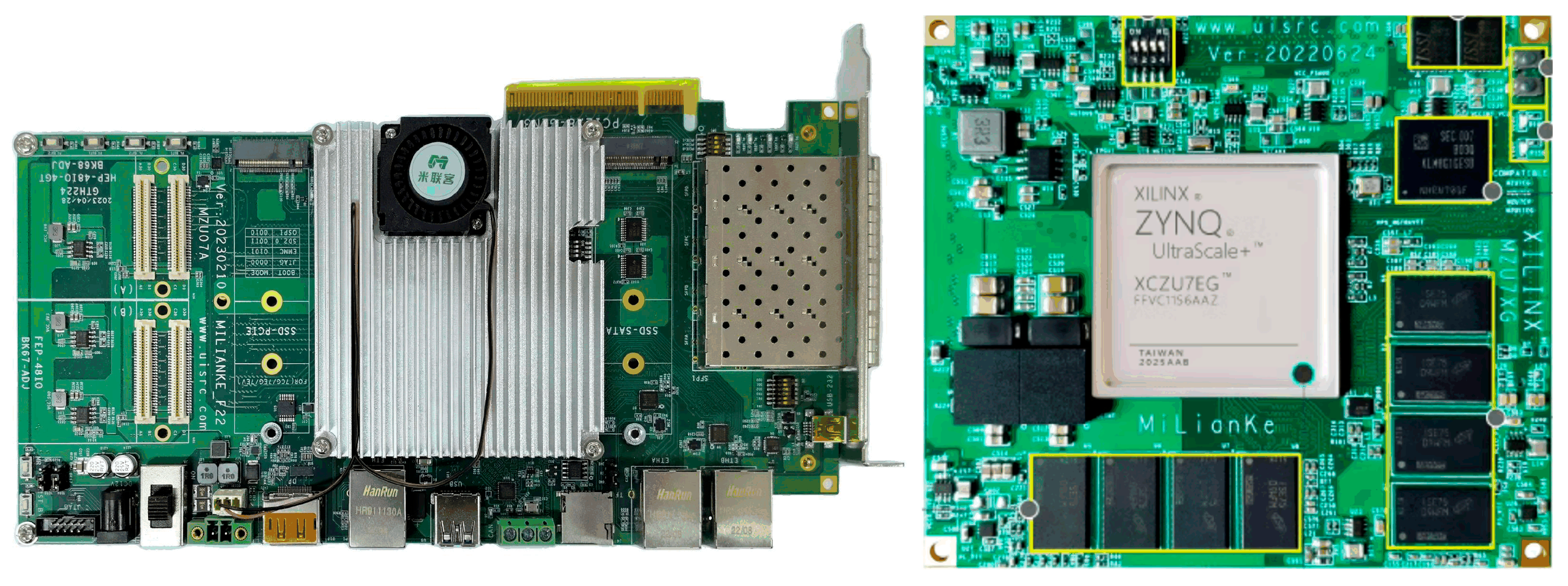
Table 6. The hardware implementation method was designed for the ZYNQ UltraScale+ XCZU7EV-2FFVC1156I (Produced by Xilinx, Inc. (now part of AMD), San Jose, CA, USA.) chip hardware platform, as shown in
Figure 14. Convolution functionality was realized by designing a timing array using Verilog. The Xilinx Vitis AI tool converts ONNX to a DPU-executable format to obtain the HDL model, which is then simulated and validated in Vivado. Experimental tools and corresponding versions are listed in the table below.
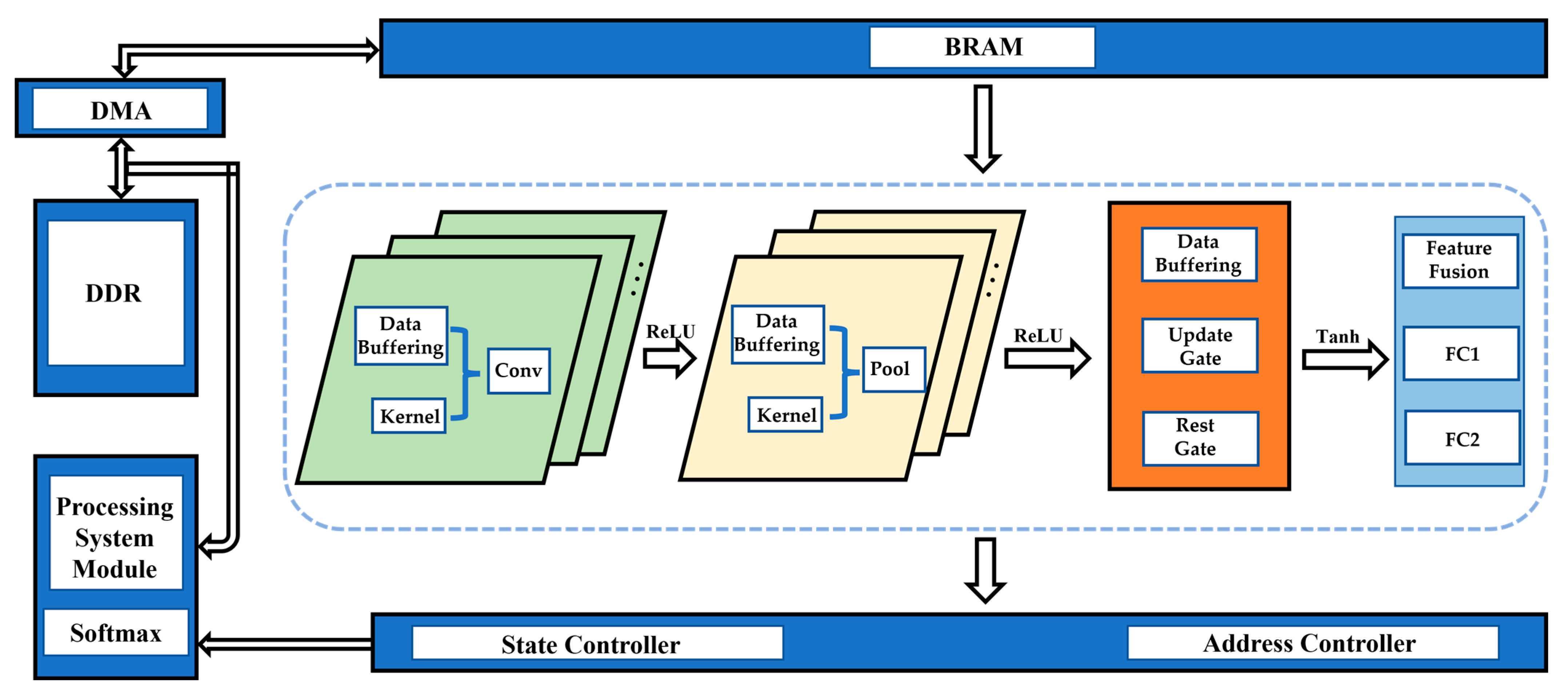
The FPGA acceleration architecture is shown in
Figure 15. Based on the independence between the layers of the 1D-CNN, the design includes three components: model parameter quantization, storage module, and computation module.
In neural network hardware implementation, data type choice is critical for computational performance and hardware resource use. Software-based network training typically uses floating-point numbers (e.g., Pytorch represents neural network weights as floating-point numbers) due to their precision and wide numerical range. However, in hardware, floating-point advantages become drawbacks:
Computational complexity: Floating-point operations involve complex hardware calculations and longer computation times;
Hardware resource consumption: Floating-point calculations require more multipliers, adders, and other hardware resources, increasing hardware resource usage;
Storage space requirements: Floating-point numbers occupy more storage space, requiring more storage units;
Time delay: Floating-point calculations can cause greater time delays.
In contrast, fixed-point numbers, though with smaller range and lower precision than floating-point numbers, enhance computational efficiency and reduce hardware resource consumption. Thus, fixed-point numbers are more common in hardware design, especially on FPGA-based deep learning acceleration platforms. This paper uses 16-bit fixed-point numbers to represent neural network parameters. The specific settings are as follows:
Bit width: 16-bit, with 1 bit for the sign, 6 bits for the integer part, and 9 bits for the fractional part.
Numerical range: The decimal numerical range of this fixed-point number is from −64 to 63.998046875.
Maximum precision: The maximum precision of the fixed-point number is approximately 0.00195.
Quantization process: The conversion of floating-point numbers to fixed-point numbers involves three steps: calculating the quantization step size, performing the quantization calculation, and executing the binary conversion. The specific method is as follows:
where
is the size of the fractional part,
represents the original high-precision value in continuous space,
denotes the quantized data in discrete space,
indicates the quantization step size,
is the rounding function, and
is the binary conversion result.
In this paper, is selected to fix the decimal point position at 6. This ensures that the quantization process balances precision and range. As the quantization parameter increases, precision improves, but the representable numerical range decreases. Conversely, a smaller reduces precision but increases the representable numerical range. After converting the floating-point parameters to fixed-point numbers through quantization, efficient storage is achieved, and the calculation process on FPGA is significantly accelerated.
To efficiently implement 1DCNN-GRU for processing plant electrical signals on FPGA, a storage structure combining Double Data Rate SDRAM (DDR), Direct Memory Access (DMA), and Block Random Access Memory (BRAM) is used. The quantized convolutional kernel weights and biases are stored in DDR, while the input feature matrix is stored in BRAM to ensure fast parallel computation. BRAM is utilized to store input data due to its high data bandwidth, enabling more efficient data access and computation. At the same time, the quantized convolutional kernel weights and biases are stored in DDR, allowing a large set of parameters to be loaded into the FPGA and ensuring that these data can be quickly transferred to BRAM for computation when needed. Since Verilog does not support direct definition of two-dimensional arrays, a one-dimensional register array is used to replace the two-dimensional structure, with horizontal and vertical counters controlling the data access sequence to achieve efficient convolution operation execution. During the convolution operation, the kernel weights and input feature matrix of each layer are transferred from DDR to BRAM via DMA technology for parallel processing, significantly reducing the CPU load and improving data transfer efficiency. The output feature matrix is then stored back in BRAM to serve as the input data for the next layer.
The core of the entire computation module is the convolution module, which is designed using a sequential array approach in this paper. As shown in
Figure 16, the convolution kernel weights are preloaded into the Processing Elements (PEs), and data flows through the PEs under the control of the clock, with the convolution multiply–accumulate results obtained at the end of the array. This design supports efficient parallel processing, where each PE can simultaneously process different parts of the data. Data only interacts with the external environment at the first and last PEs. The expression for a single processing element is given by Formula (13):
where
represents the output of the previous multiply–accumulate unit;
is the input data;
fand denotes the convolution kernel weights bound to the processing element.
The simulation results of the convolution module are presented in
Figure 17. In this figure,
denotes the clock signal,
represents the reset signal, and
stands for the input enable signal. Input data is read from the memory module into the convolution module. When the
signal is at a high level, the convolution module fetches weight parameters from the Block Random Access Memory (BRAM) and conducts convolution computation. Eventually, the result is divided into an integer part (
) and a decimal part (
), and a floating-point format (
) is also provided for validation. The signals
and
indicate the addresses of the input and weight memories, respectively, while
and
correspond to the input and weight values. The simulation demonstrates the dynamic variations in these signals during operation, which elucidates the data flow and processing within the convolution module.

