Article

Design Assessment of Power Supply Systems for Divertor Coils in the Divertor Tokamak Test

1
Dipartimento Energia “G.Ferraris” Politecnico di Torino, 10129 Torino, Italy
2
DTT S.c. a.r.l., National Agency for New Technologies, Energy and Sustainable Economic Development (ENEA), 00044 Frascati, Italy
*
Author to whom correspondence should be addressed.
Appl. Sci. 2025, 15(19), 10441; https://doi.org/10.3390/app151910441
Submission received: 20 July 2025 / Revised: 17 September 2025 / Accepted: 20 September 2025 / Published: 26 September 2025
(This article belongs to the Section Energy Science and Technology)

Abstract

In tokamak-based nuclear fusion systems, powering the coils to control the plasma is a challenge that involves design choices that are a mix between advanced and traditional approaches. Each tokamak coil requires peculiar driving conditions and needs specific design activities. This paper deals with power supply design assessment for the Divertor (DIV) Coils in the Divertor Tokamak Test (DTT) facility. The design constraints of high-current (5500 A) and relatively low-voltages lead to the comparison of an SCR-based AC–AC converter (cycloconverter) with an IGBT-based DC–AC inverter with devices in a parallel solution and with interleaved modulation. The design assessment of two converter solutions to drive the DIV coils with the control issues were explored and described. Several simulation results were carried out to define the DIV coils operative conditions. Furthermore, an electro-thermal analysis on the used IGBT or thyristor devices was carried out considering the losses and the highest temperatures obtained in the conditions of maximum stress for the components.

1. Introduction

Nuclear fusion may potentially be the perfect solution for the problem of producing energy under sustainable conditions [1]. Despite the many scientific and technical difficulties encountered over the years, the worldwide interest is surprisingly growing, leading to the construction of several new experiments, involving both public institutions [1] and private companies [2]. Each of these experiments is based on a specific approach to implement fusion and may focus on specific aspects of research and engineering. According to the European Roadmap to the Realisation of Fusion Energy [1], the most noticeable facility under construction is the international project ITER [3], focused on demonstrating the scientific and technological feasibility of fusion power at a large scale. ITER is expected to provide the design and operative information for the future Demonstration Power Plant (DEMO) [4,5].
The approach that is most explored to produce energy is based on the concentration of the fusion reactions in an ionized gas (plasma) confined by strong magnetic fields (magnetic-confinement fusion), induced by coils carrying high currents. In particular, the most promising configuration of the magnetic field is known as tokamak [6]. For example, ITER is designed as a tokamak. Within a tokamak, hydrogen isotopes are magnetically confined and heated to temperatures exceeding 100 million degrees Celsius to form plasma.
A tokamak requires a range of power supply (PS) systems to produce the high currents and associated magnetic fields needed for operation [6,7]. Each tokamak coil is characterized by different specifications in terms of current, voltage, dynamic response, duration, etc.
The Divertor Tokamak Test (DTT) facility, currently under construction in Frascati, Italy, is a collaborative effort primarily led by the Italian government-sponsored research and development agency ENEA and supported by the EUROfusion program [8,9]. While ITER focuses on the scientific and technological feasibility of fusion, DTT is specifically engineered to explore and validate advanced configurations and new materials, under conditions relevant to DEMO, to bridge the gap between current experimental devices and future power plants. Its successful operation is expected to significantly accelerate the development of fusion as a viable and sustainable energy source for the planet.
Even though DTT is a cutting-edge tokamak that can support many activities, it has been mainly designed to address one of the most critical issues for future fusion power plants: the handling of extreme thermal loads on the divertor [10]. The divertor is a specialized region within the tokamak chamber where magnetic field lines are intentionally shaped and guided. This configuration creates a dedicated “channel” through which plasma thermal power as well as fusion ashes and impurities are conveyed and exhausted away from the main plasma and the sensitive chamber walls. This function is paramount for maintaining the stability and integrity of the plasma, protecting in-vessel components from excessive heat loads, and ultimately ensuring the long-term operations and safety of future fusion reactors. The divertor is a crucial component for fusion, independently of the other specific design aspects. DTT will allow researchers to investigate various magnetic configurations and plasma-facing components, that can withstand the extreme power fluxes and the harsh conditions expected in a commercial fusion reactor, which can be comparable to the heat flux on the surface of the Sun.
Since DTT aims to serve as a testbed for several divertor solutions under different conditions [11,12,13], its design must be as flexible as possible. In particular, this flexibility must be achieved for the magnetic system and its PSs. This is very critical for a complex device like a tokamak. The initial step in designing any tokamak PS system involves choosing between established and innovative solutions [7]. While conventional approaches are generally preferred for ensuring faster and safer completion of the DTT project, several technical challenges are still present and require new solutions.
Previous papers presented the function and design of some DTT coils and related PSs [7,14,15,16]. This paper focuses on the PSs for the DTT divertor (DIV) coils. These coils are placed inside the vacuum vessel, close to the divertor region to shape the field and plasma configurations [17]. It is evident that such coils are essential for the objectives and operations of DTT, involving complexities and critical issues that must be addressed to achieve its scientific objectives and advance tokamak technology.
After a general overview of the DTT magnetic system, Section 2 presents the characteristics of the DIV coils and the requirements for their operations. The PSs designed to satisfy these requirements are introduced in Section 3. To this aim, the possible PS topologies (IGBT inverter and 12-pulse cycloconverter) are presented and compared. Section 3.1 adopts for the IGBT inverter the same topology already proposed for other DTT coils [14,15], in order to simplify the practical implementation. With this approach, the same power electronic modules could be used for all coils, with different connections and different numbers of modules in series and parallel. Section 3.2 presents the design for a thyristor (SCR) cycloconverter. The results of the electrical simulations and of the electrothermal analysis for the two options are reported in Section 4 and Section 5, respectively. Finally, considerations on the PS systems are carried out and conclusions are drawn.

2. Overview of the DIV Coils System

2.1. Components of the DTT Magnet System

The magnetic system is the fulcrum of the DTT operations. It is a complex and integrated network designed for both robust plasma confinement and highly flexible control, especially concerning the critical divertor region. The magnetic field in the center of the plasma is 6 T, comparable with that of ITER [5,8].
The DTT coils and their main functions are listed as follows [7,8].
  • Toroidal Field (TF) Coils: Generate the primary toroidal magnetic field.
  • Poloidal Field (PF) Coils: Control plasma shape, position, and stability.
  • Central Solenoid (CS): Induces the plasma current.
  • Vertical Stability (VS) Coils: Provide fast vertical stabilization and radial control of the plasma.
  • Divertor (DIV) Coils: Offer fine-tuning of the magnetic field in the divertor region for heat exhaust management and advanced divertor configurations.
  • Non-Axisymmetric (NA) Coils: Could be used for advanced plasma control, such as Edge Localized Mode (ELM) mitigation.
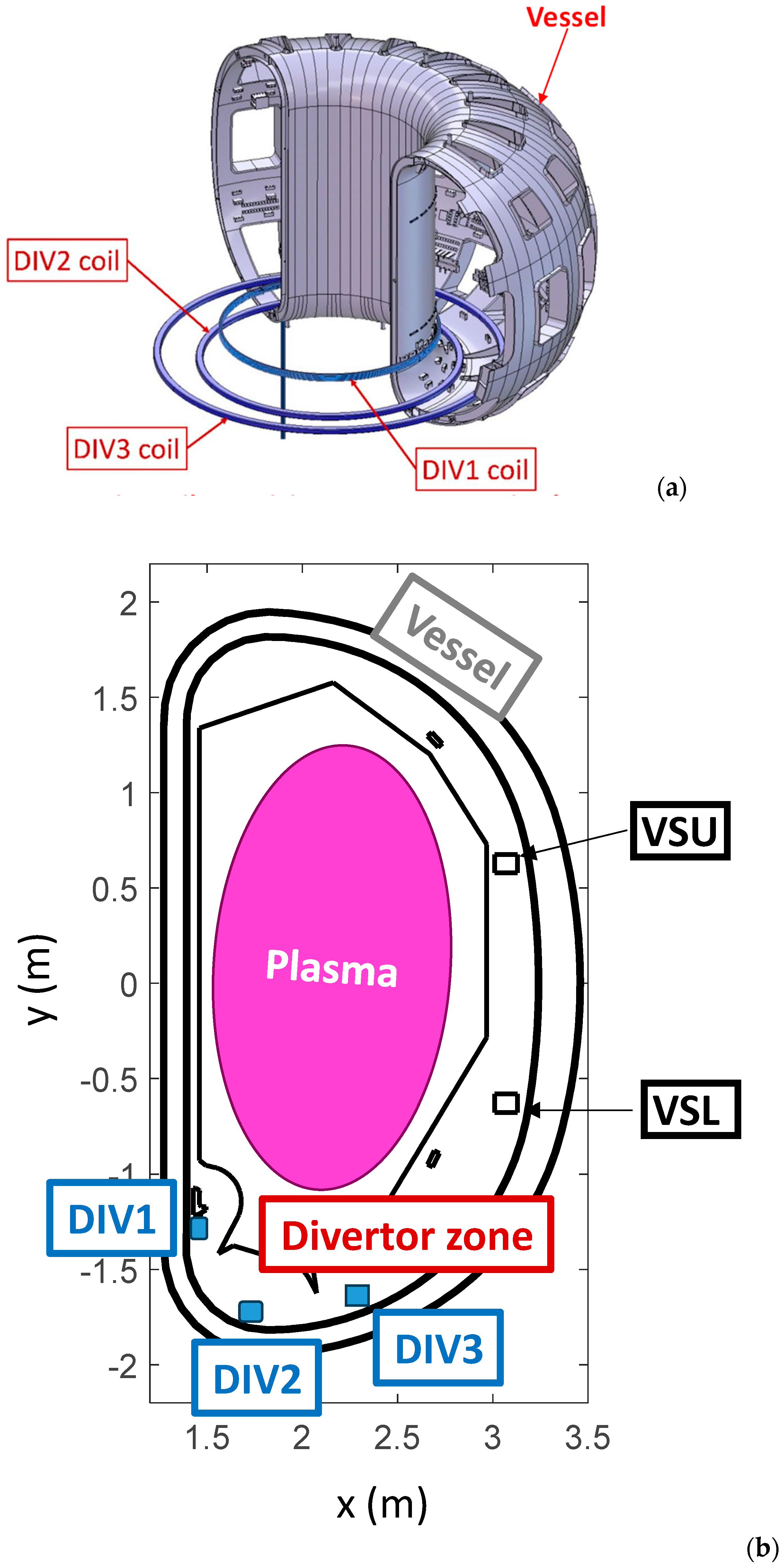
The first three types of coils (TF, PF, and CS) are superconducting, operating at cryogenic temperatures [8]. The remaining three coils (VS, DIV, NA) are in copper and placed inside the vacuum vessel, as shown in Figure 1 and Figure 2.

2.2. Characteristics of the DIV Coils

The DTT design includes three DIV coils, classified as DIV1, DIV2, and DIV3, respectively, that will be independently controlled. Figure 2 sketches the configuration of the DIV coils, by showing a 3D view and a cross-section of the DTT vessel.
The main issues in the design of the DIV coil PSs are summarized in the following:
  • The primary function of DIV coils is to enable accurate control of the desired magnetic configuration (that is not unique in DTT [11,12,13]), shaped by quasi-static fields.
  • Even though a high number of DIV coils could increase the degrees of freedom in field shaping, a trade-off must be identified due to the space constraints in the divertor region and to the mechanical loads. In fact, the DIV4 coil and the further separated turns in the DIV1 coil, present in the previous designs, were removed, as the simulations showed a limited improvement in plasma interaction with respect to the assumed configuration [17].
  • The static spread of the plasma impinging on the divertor plates may not be sufficient to achieve safe thermal loads. Therefore, strike-point sweeping (wobbling) is proposed as a strategy to further reduce them [18]. It consists of enlarging the affected area by imposing a periodic movement of the plasma at a desired frequency without significant changes of the plasma boundary. For the most probable and investigated configurations, the effect is significant up to 10 Hz, with an expected optimization around 4 Hz [17].
  • As the DIV coils are placed inside the vessel, unexpected plasma instabilities, in particular those classified as plasma disruptions, can produce high induced currents in the DIV circuits [17]. In practice, such disruptions are a relevant driver for coil and PS design. Even though several solutions were studied to address this problem [19], the protection solution identified for DTT consisted in inserting additional inductances in each DIV circuit that will be in series with the original load coil [17].
The main specifications for the PSs of the DIV coils are as follows:
  • Maximum DIV coil current Imax = 5.5 kA.
  • DIV coils required voltage 500 V (DIV1, DIV2); 1700 V (DIV3).
  • 4-quadrant operation.
  • Maximum required bandwidth of current control is below 10 Hz (typical value 4 Hz).
It is worth noting that the maximum bandwidth for the DIV PSs is 4 Hz. SCR-based converters could power these coils with well-known topologies. From these operative conditions, low-frequency constraint, the design based on H-bridges, is worth comparing with the SCR-based cycloconverter.

3. DIV Coil Power Supply Arrangement

The PS system dedicated to the DTT DIV coils is composed of three independent 4-quadrant power converters. Each of these units is engineered to deliver a limit current of 5.5 kA and operate with a voltage rating of 0.5 kV and 1700 V (reported in Table 1) at low frequency (f0 = 4 Hz). The implementation of 4-quadrant operation is a critical design feature, allowing for bidirectional current flow and voltage polarity reversal. This capability is indispensable for achieving the rapid and precise control of magnetic fields and coil currents required for dynamic plasma shaping, active feedback control, and effective strike point manipulation, which are central to DTT experimental flexibility. The DIV coils request dynamic responsiveness and precise control of both lower voltage and current levels compared to VS coils [15], enabling active plasma shaping and heat exhaust mitigation.

3.1. Full-Bridge IGBT-Based Solution

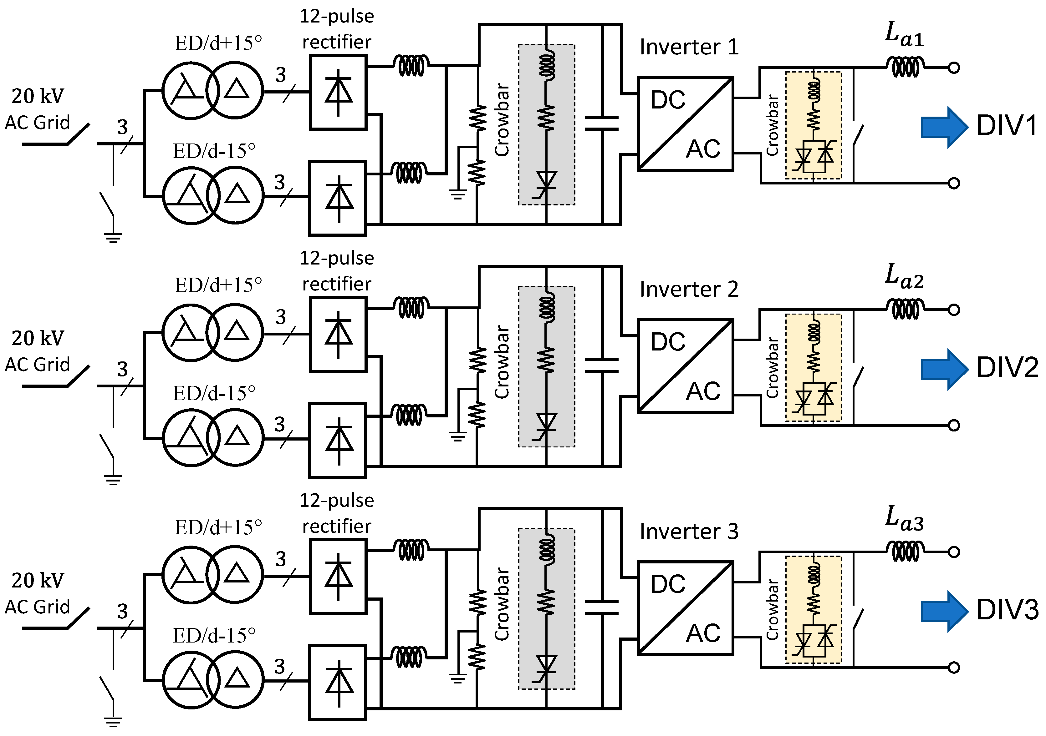
The topology of power supply for each DIV coil is shown in Figure 3. The proposed topology solution uses three independent PS units. Each unit consists of the following:
  • 12-pulse rectifier fed by two transformers employing extended delta–delta configurations (ED/d + 15° and ED/d-15°, respectively) [7,14]. The rectifier is obtained by connecting two or more diode rectifier units in parallel.
  • Single phase DC/AC converter using IGBT technology to supply the DIV coils through additional inductors that are needed to limit the current in case of disruption. The IGBT technology allows very low response times to be obtained with respect to SCR technology. Having low response times is crucial in case of disruption, where the converter must be turned off quickly.
  • Crowbars for protection both on the DC link (discharge breaker) and at the output of the DC/AC converter.
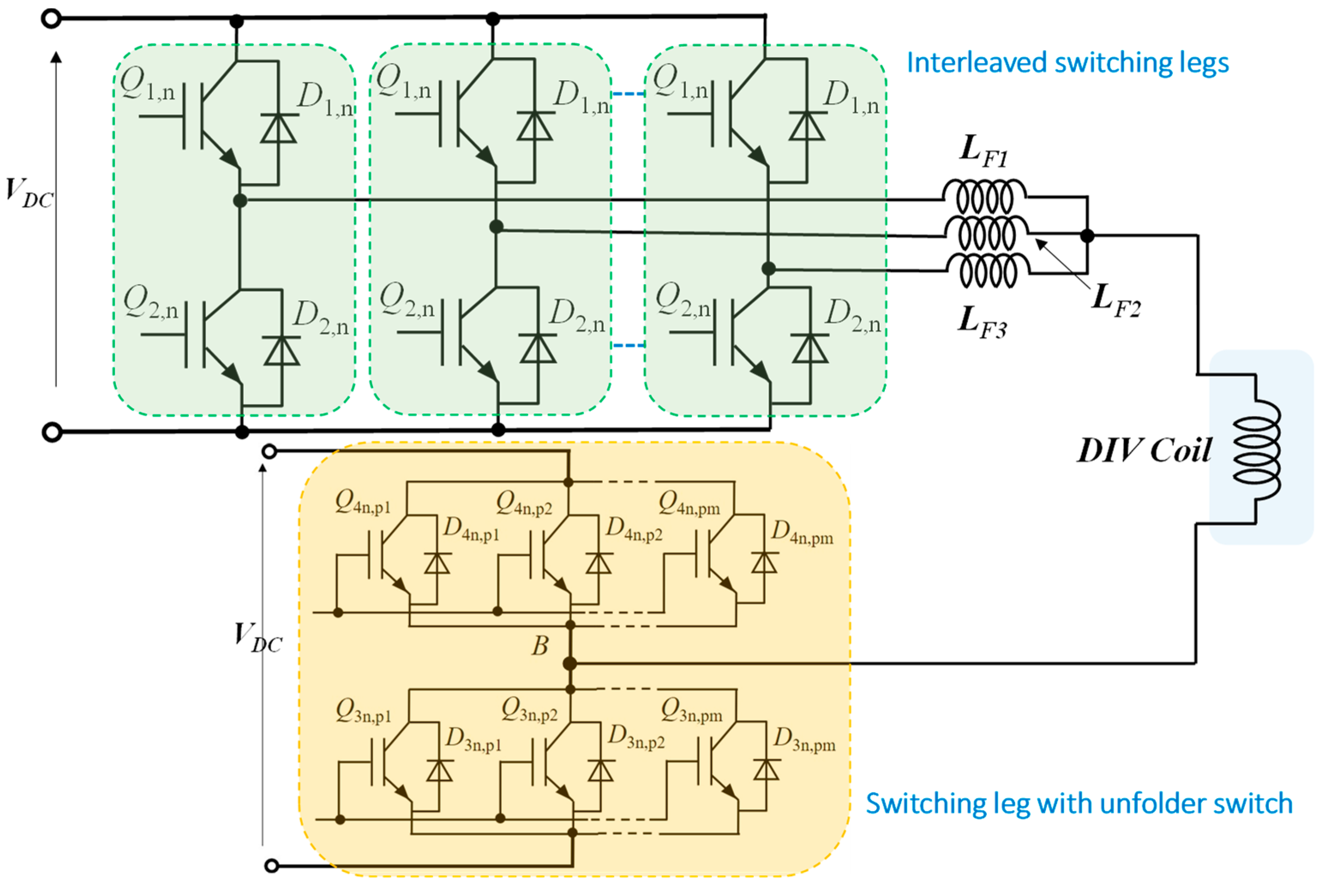
The internal scheme of one single inverter unit is shown in Figure 4. Each phase consists of several legs connected in parallel through inductors. Starting with an analysis of the available IGBT solutions on the market, the main characteristics of the DIV maximum current and voltage requested for each coil and the IGBT solution are reported in Table 1.
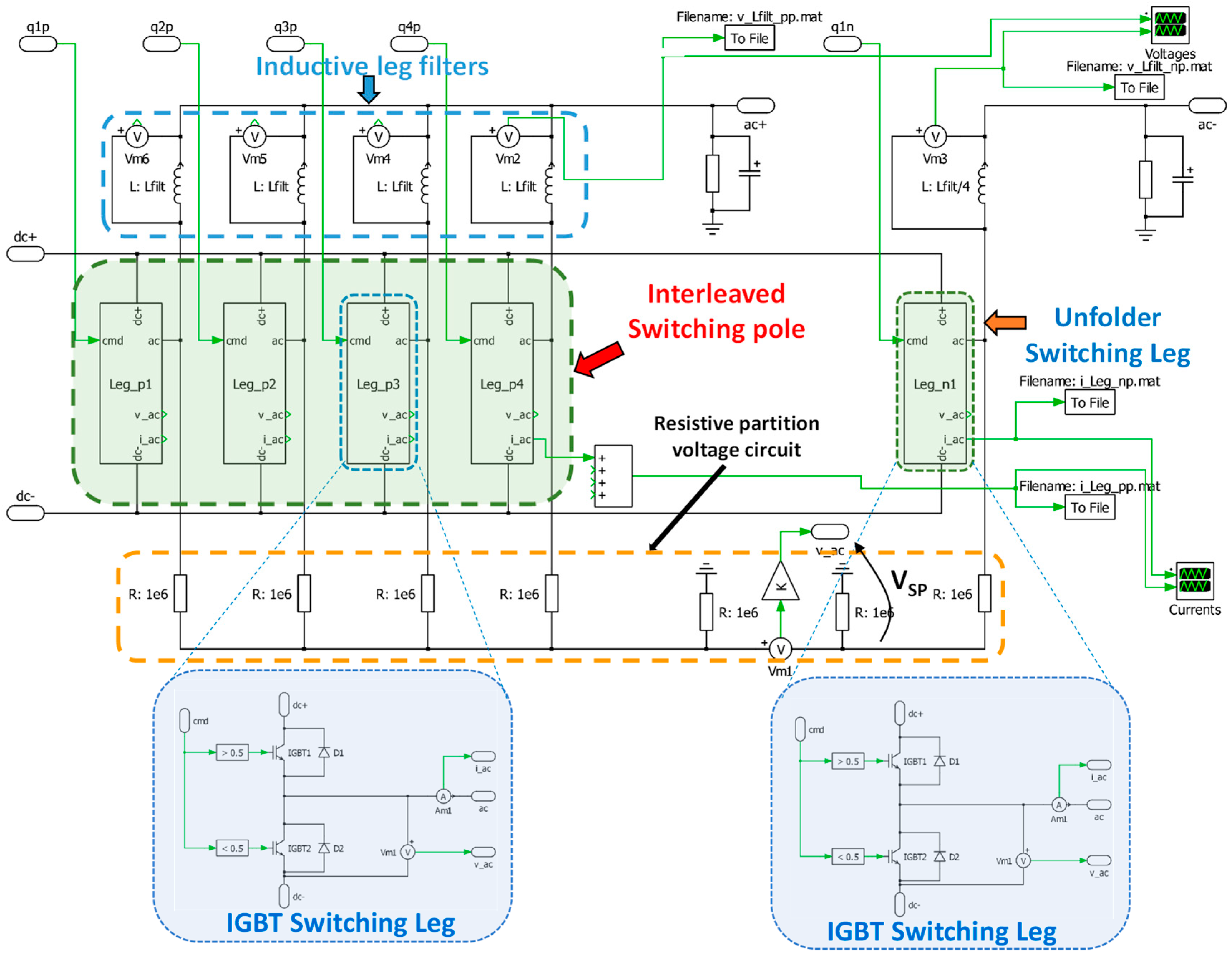
To reduce switching losses, the full-bridge DC–AC proposed IGBT-based solution reported in Figure 4 is composed of an inverter with multiple legs operating in interleaving connection and an unfolding leg.
In Figure 4, a general view of n interleaved switching legs with the coupling inductor LF to avoid circulating current and a switch composed of n parallel IGBTs for the un-folding switching leg is shown.
In the interleaving approach, multiple switching legs (or channels) operate in parallel with a control technique where their switching gate signals are phase-shifted evenly over the PWM switching period [20]. The unfolding leg is composed of a high-side and a low-side switch (see the low-side of Figure 4). The unfolder devices switch at the fundamental output frequency (4 Hz), so their switching losses are negligible. With this control strategy, the interleaving legs operate to obtain the requested PWM modulation, while the unfolding switching leg achieves the bipolar voltage operation for the full-bridge [21]. In the interleaving switching legs the command signals of the switches generated by the modulation strategy are supplied to each switching leg with a phase shift (PS) concerning the other legs as:
P S = 360 N C
where NC is the number of legs. The results of Equation (1) give the angle of phase shift based on the number of legs chosen to meet the current rating of the available IGBTs. The interleaving solution has the advantage of providing a multilevel output voltage with an equivalent frequency that is NC times higher than the switching frequency of the single leg. The higher output current frequency features a lower current ripple level, resulting in a reduction of the output filter requirement. Furthermore, a lower ripple current reduces conduction and switching losses in the devices and allows for smaller filter inductors and capacitors, improving overall efficiency. Moreover, multiple phases share the total load current, enabling the converter to handle higher power levels without overstressing a single phase [22]. The combined use of interleaved approach and unfolding switching leg solution improve the simplicity of the converter topology and the system reliability [15].
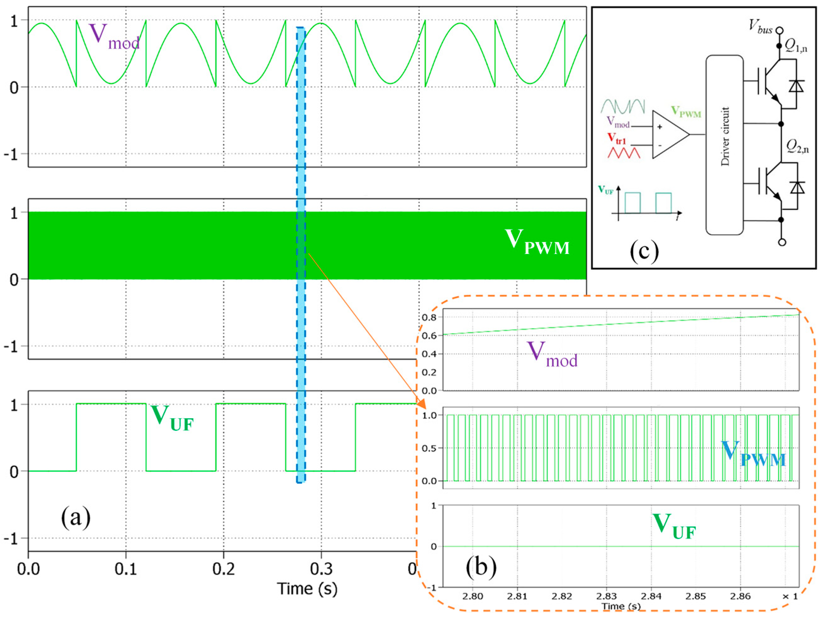
The modulation strategy is obtained by comparing the sinusoidal modified voltage modulation signal Vmod (Figure 5a) with four triangular waveforms with 90 degrees of phase shift according to the interleaving strategy and Equation (1) for four interleaved switching legs.
The PWM signal for a switching leg (VPWM) is reported in Figure 5a while the zoomed view is shown in Figure 5b. The principle schematic of the PWM control strategy is depicted in Figure 5c. The unfold command signal (VUF) with duty-cycle (D) of 50% is also reported in Figure 5a [15].

Inverter IGBT Selection

The four switching legs for the interleaved connection are composed of modules with a current rating of 1800 A, capable of reaching a total maximum of 7200 A, with a safe margin of respect to the 5 kA requested. The switches’ selection is based on a switching leg module. The voltage of 2300 V (FF1800R23IE7 by Infineon [23]) features a safe margin for the peak maximum voltage required by the coils DIV1, DIV2, and DIV3. In the unfolder switch, the IGBT modules are in parallel connection.

3.2. Cycloconverter Tyristor-Based Solution

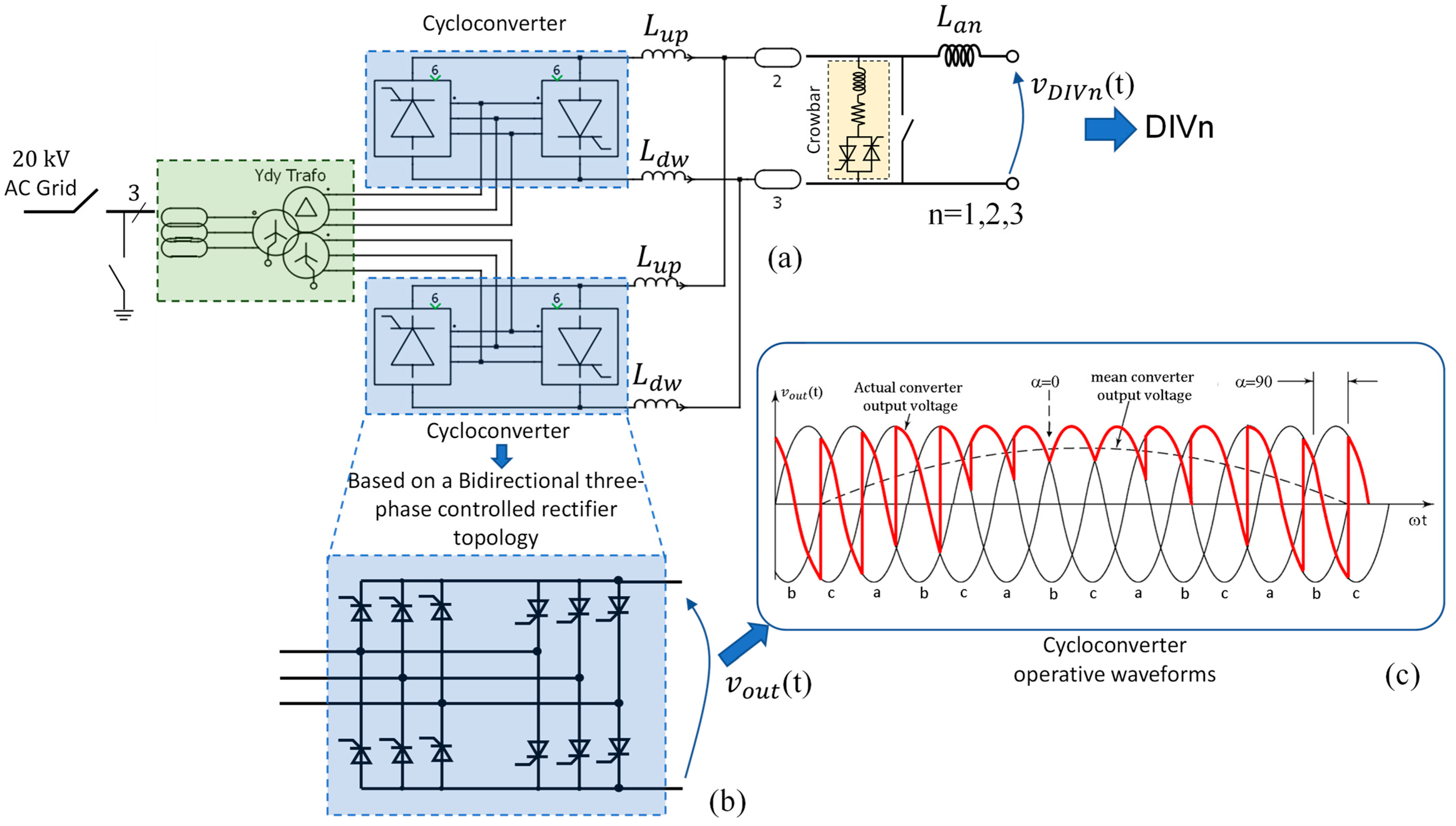
A 12-pulse cycloconverter system is fundamentally designed to achieve superior input current harmonic mitigation, characteristic of a 12-pulse rectifier. This is typically accomplished by employing two 6-pulse converter bridges, each fed by a three-phase AC source that is phase-shifted relative to the other. The phase shift, usually 30 degrees, is critically generated by phase-shifting transformers, such as a combination of a star-star and a star-delta transformer. This converter solution is well known in power electronics scenarios and several papers describe the topology operations [24,25]. This arrangement ensures that the harmonics generated by one 6-pulse bridge are out of phase with those from the other, leading to the cancellation of specific low-order harmonics (e.g., 5th, 7th, 17th, 19th) from the overall input current waveform. This configuration is particularly beneficial for high-power applications where strict adherence to power quality standards is required. Furthermore, a significant advantage is the elimination of an intermediate DC link compared with an inverter solution. This design choice leads to higher overall efficiency by removing the losses associated with DC link components like large filter inductors and capacitors.
The implementation of a 12-pulse input configuration, while significantly improving input current quality and ensuring compliance with standards, inherently increases the complexity and cost of the overall system. This is due to the requirement for multiple specialized transformers and a larger number of semiconductor switches compared to simpler 6-pulse systems. For instance, a 12-pulse system often involves two sets of three-phase rectifiers, each requiring its own set of SCRs, and the associated control circuitry becomes more intricate to manage the precise firing angles and synchronization across these numerous devices. This increased hardware complexity, size, and expense represent a critical design consideration and a trade-off for the enhanced power quality benefits.
The successful operation of a 12-pulse cycloconverter with single-phase output is based on the following key components.
  • Thyristors (SCRs): These are the primary power semiconductor switches used due to their high-power handling capability and suitability for line (natural) commutation in step-down cycloconverter operations. The large number of SCRs required, especially in multi-pulse configurations, is a defining characteristic of these systems.
  • Phase-Shifting Transformers: These are crucial for creating the 12-pulse input characteristic. Transformer arrangement provides the necessary phase displacement (e.g., 30 degrees) between the two sets of three-phase voltages feeding the 6-pulse converter bridges, enabling the cancellation of specific input harmonics. Additionally, they offer galvanic isolation and can step voltage up or down as required for the application.
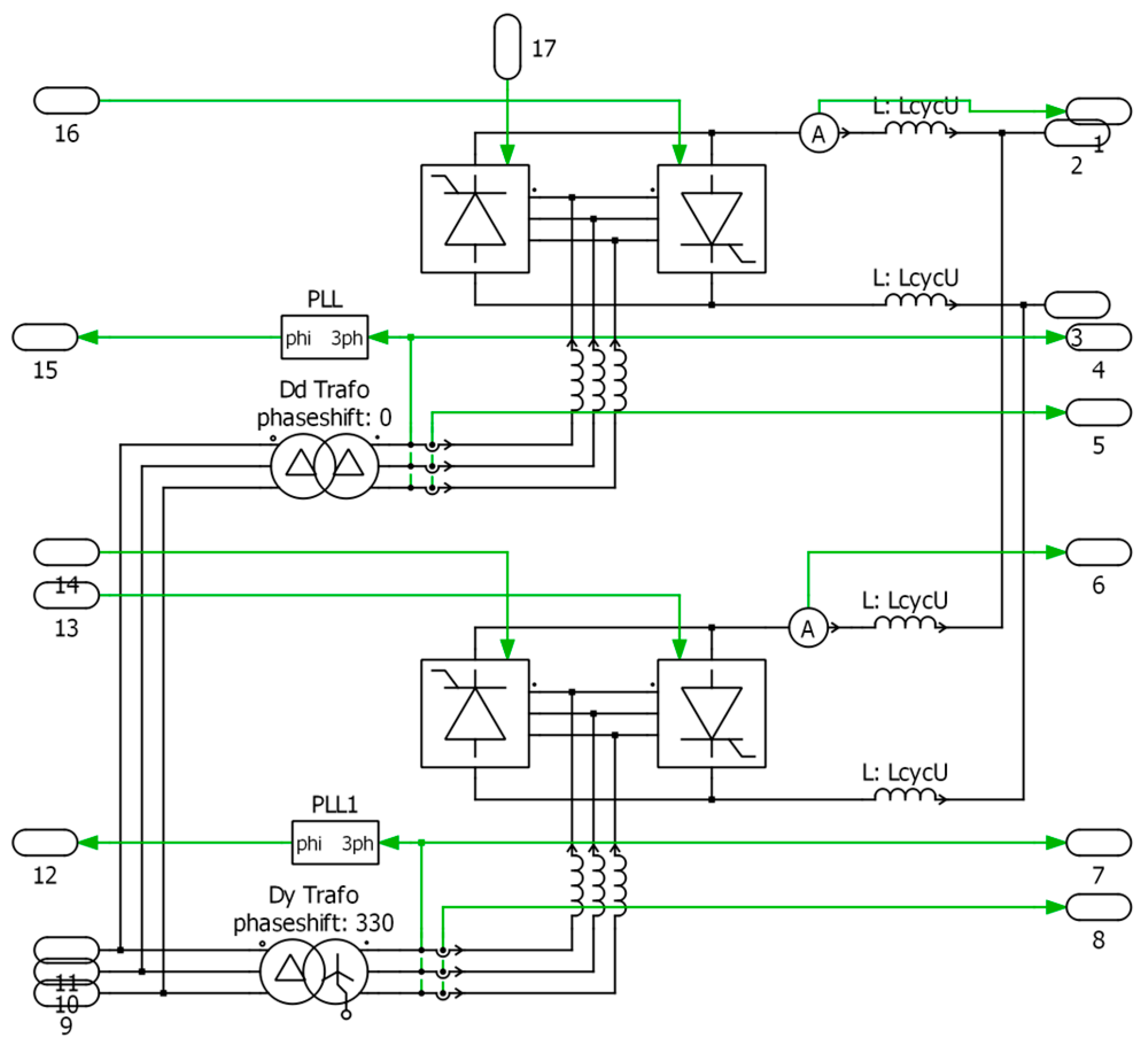
In Figure 5 a 12-pulse cycloconverter topology arranged for the DIV supply is shown. The circuital topology is composed of two 6-pulse bidirectional converters supplied by a star-delta transformer configuration, as shown in Figure 6a. In Figure 6b, the bidirectional 6-pulse three-phase topology is focused. Finally, in Figure 6b, the 12-pulse cycloconverter qualitative output voltage for the positive half-wave is depicted. The topology without a circulating current was chosen.
Cycloconverters synthesize the output AC waveform by selecting and regulating segments of the input AC voltage through accurate control of the SCR firing angles. The firing angles are suitably varied to create the desired output voltage and frequency, approximating a sine wave from the input segments. When feeding an inductive load, the cycloconverter’s behavior is significantly influenced by the load’s characteristics. Inductive loads, with large inductance, inherently tend to smooth the output current waveform, often leading to continuous current flow, which is generally desirable for stable operation. However, if the load inductance is insufficient, the current can become discontinuous; in this case the control system is more complex. But in the case of DIV coils, the inductors are of sufficiently large value. A major consequence of inductive loads is the introduction of a lagging power factor, where the current waveform lags the voltage waveform [26].

Cycloconverter SCR Selection

An SCR with high-power handling capability is requested to drive the DIV coils with the cycloconverter topology. A suitable SCR with mean on-state current, IT(AV)M = 5290 A at Tc = 70 °C and repetitive peak OFF-state voltage, VDRM = 2200 V, was chosen (T4771N22TOF by Infineon [27]).

4. Power Supply Topologies Simulation Results

This section shows the simulation results obtained with the two topologies. Voltages, currents, and current errors are shown to compare the control performance of the inverter and the cycloconverter.

4.1. IGBT-Based Inverter Electrical Simulation Results

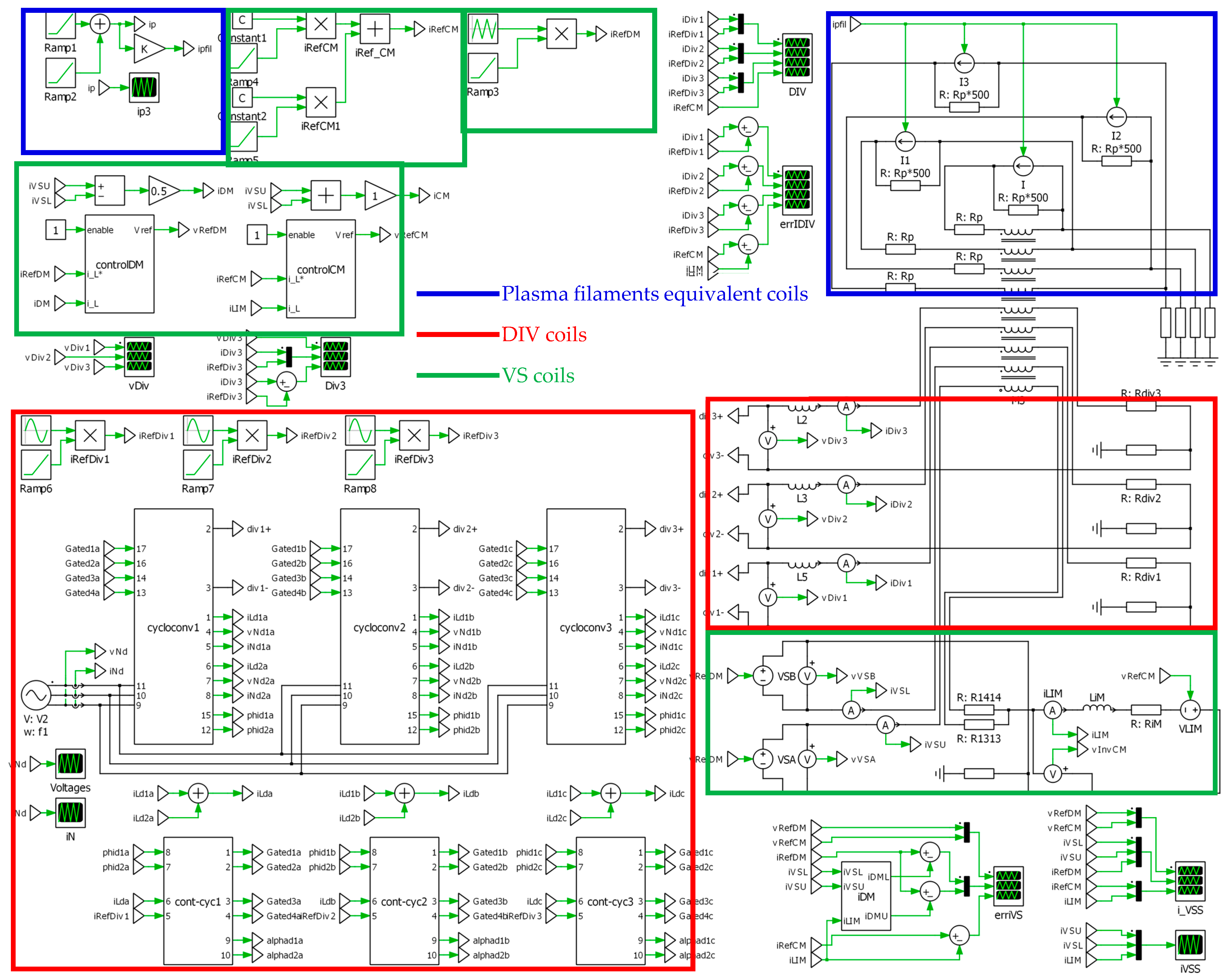
The simulation results were carried out arranging single-phase inverters in PLECS® tool. The global block scheme of the simulated circuit is reported in Figure 7. Rectangles in different colors in Figure 7 show the simulated systems: in blue, the plasma filaments equivalent coils; in red, the divertor coils (DIV1, DIV2, DIV3); in green, the vertical stabilization coils (VSL, VSU). Figure 8 shows the inverter topology simulation schematic for all of the DIV coils, composed of the four legs of the interleaved switching pole and the unfolder switching leg. The coils are simulated as a system of auto and mutual inductances whose values are given through a matrix of inductances. The generation of the coils currents is ideal for the plasma filaments, given through controlled current generators; they are considered constant (at 1.25 MA) during the simulation, so they induce no mutual emfs on the other coils; significant induced emfs would arise during disruption phenomena; for those cases the power supplies protection system would disconnect the converters from the coils to avoid damages. For the VS coils, the supply is idealized to simulate the current controlled inverters that should be used [15]; thus, the voltage references for the inverters are directly supplied to the coils through controlled voltage sources.
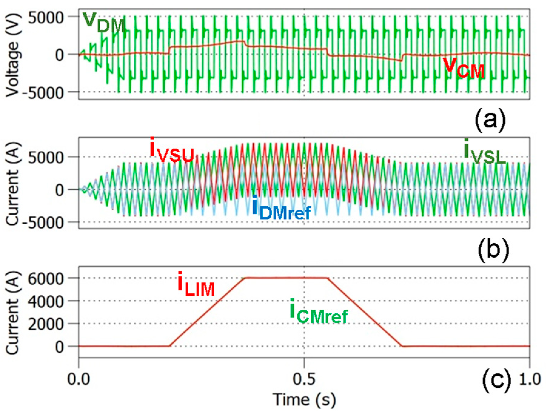
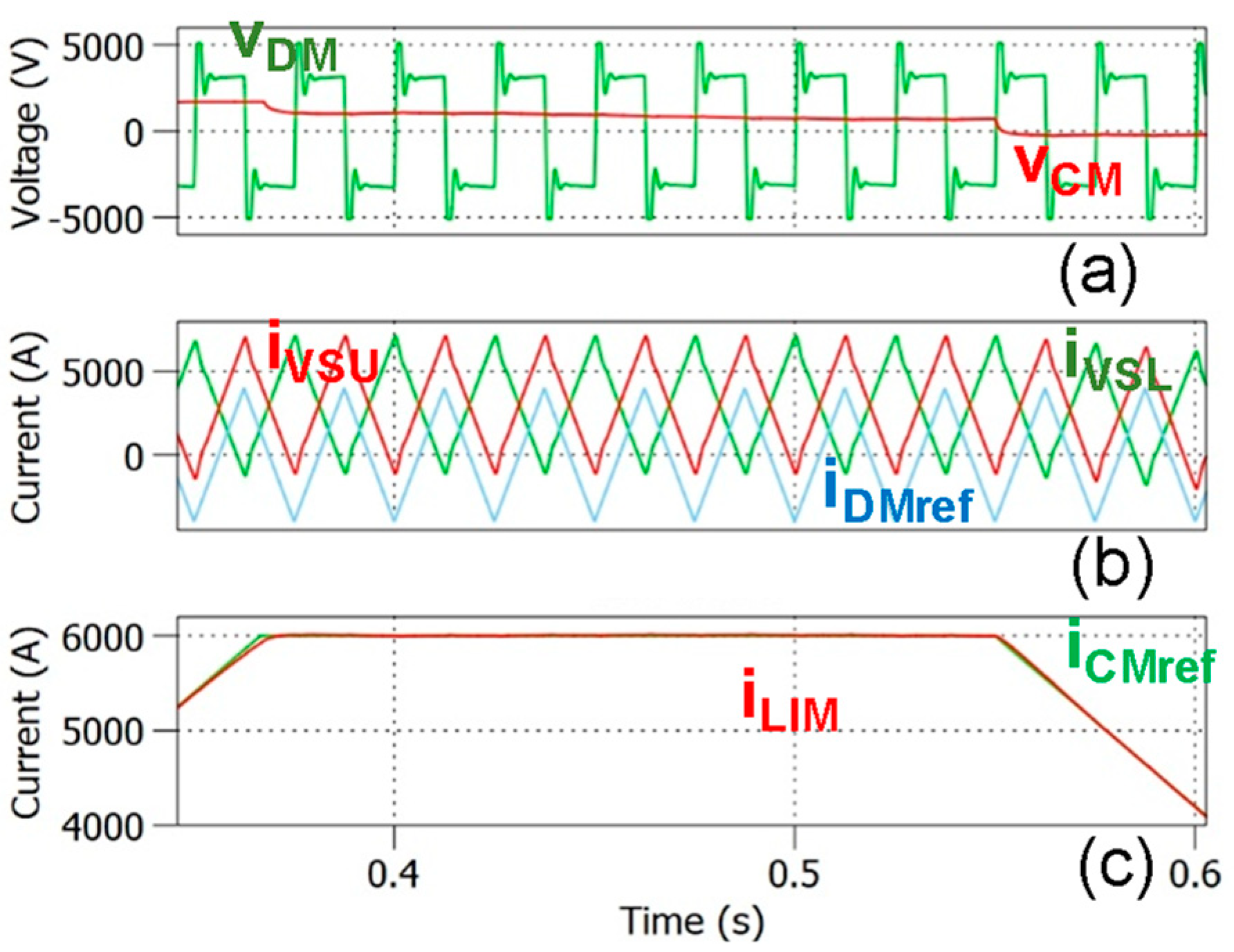
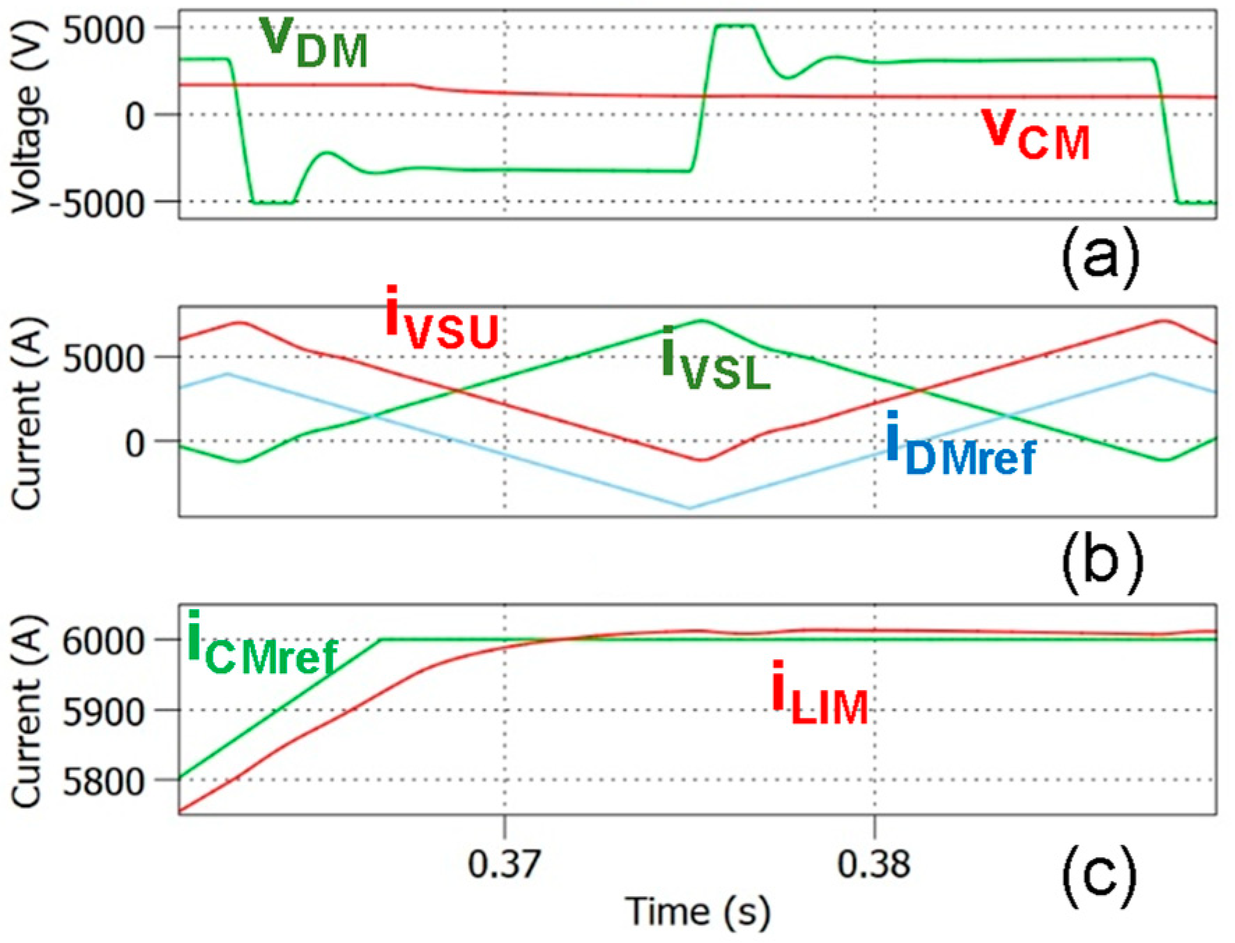
Figure 9, Figure 10 and Figure 11 show the voltages and currents of the VS coils and of the common mode inductance: In Figure 9a the output voltages of the single phase inverters for VS coils (vDM) and common mode inductance (vCM) are shown; in Figure 9b the differential mode current reference iCMref and the VS coils currents (IVSU is the current of the upper coil VSU and IVSL is the current of lower coil VSL—see Figure 2) are shown; the effect of the common mode current is to move the VS coils currents from the condition of zero average values to that in which the average values are half the common mode current; in Figure 9c the common mode current reference iCMref and common mode inductance current iLIM are shown. Figure 10 and Figure 11 show the same quantities as Figure 9, respectively, for one period of the DIV coils currents (0.25 s) and for one period of the VS coils currents. These periods were chosen when the common mode voltage reference briefly saturates at 1700 V.
For the DIV coils, actual current controlled inverters were simulated, as described in Figure 12. The IGBT model available in the PLECS® library was used to arrange the switching legs with the parameters based on the selected actual power devices.
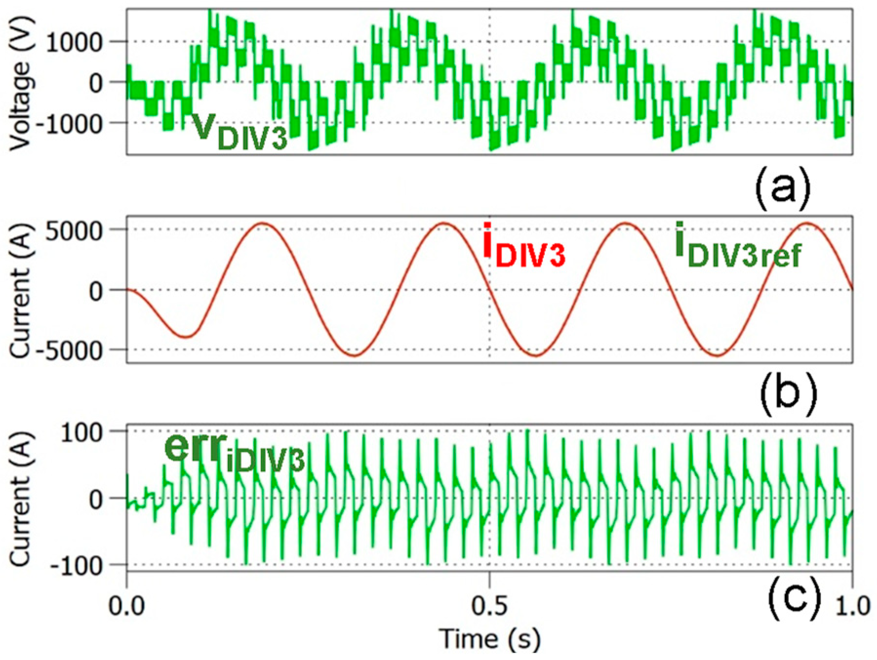
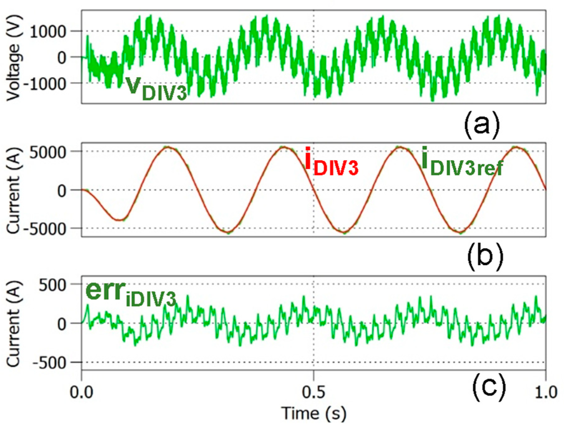
In Figure 12 the waveforms obtained for the DIV3 coil are shown; the inverter voltage vDIV3 is shown (a); then the coil current iDIV3 and its reference iDIV3ref are shown (b); finally, the current error erriDIV3 is shown (c). As can be seen in Figure 12a, there are four levels of positive voltage and four of negative voltage due to the number of interleaved legs chosen and to the unfolder strategy; the DIV3 coil requires the highest voltage among the DIV coils and the four inverter voltage levels can be seen (±1700 V for the highest level). The commutation of the unfolder switching leg determines the change of sign of the inverter output voltage [14]. The fundamental frequency is 4 Hz, and the switching frequency of each switching leg was set at 1 kHz; since the modulation triangle waveforms are phase-shifted of one quarter of period, the current ripple frequency is 4 kHz. Figure 13 shows one period (0.25 s) of the waveforms shown in Figure 12.
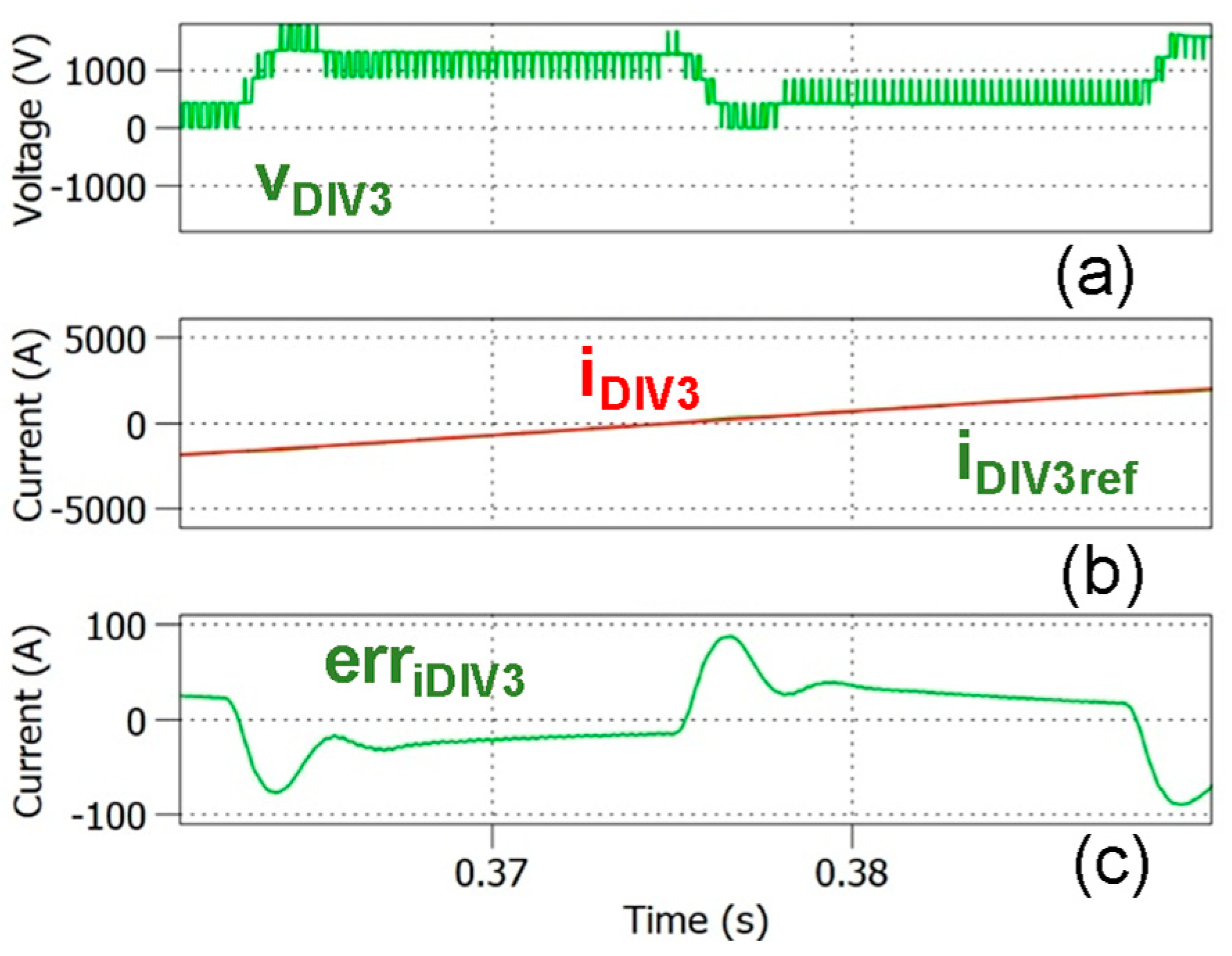
Finally, Figure 14 shows a further detail of Figure 12: since the VS coils operate at 40 Hz with triangular current waveforms [15], square wave induced emfs are induced through the mutual inductances and they are a disturbance to the current control of all other coils. Thus, the quantities during one fundamental period of the VS coils (0.025 s) are shown.
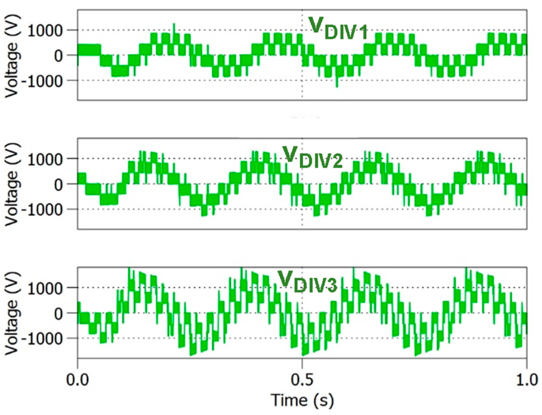
Figure 15 shows the voltages for all the DIV coils (vDIV1, vDIV2, and vDIV3); all are disturbed by the emfs induced by the VS coils operation; the most disturbed is DIV3, which is placed closer to the VS coils (Figure 2b); DIV3 also requires the highest supply voltages due to its self-inductance value.

4.2. SCR-Based Cycloconverter Electrical Simulation Results

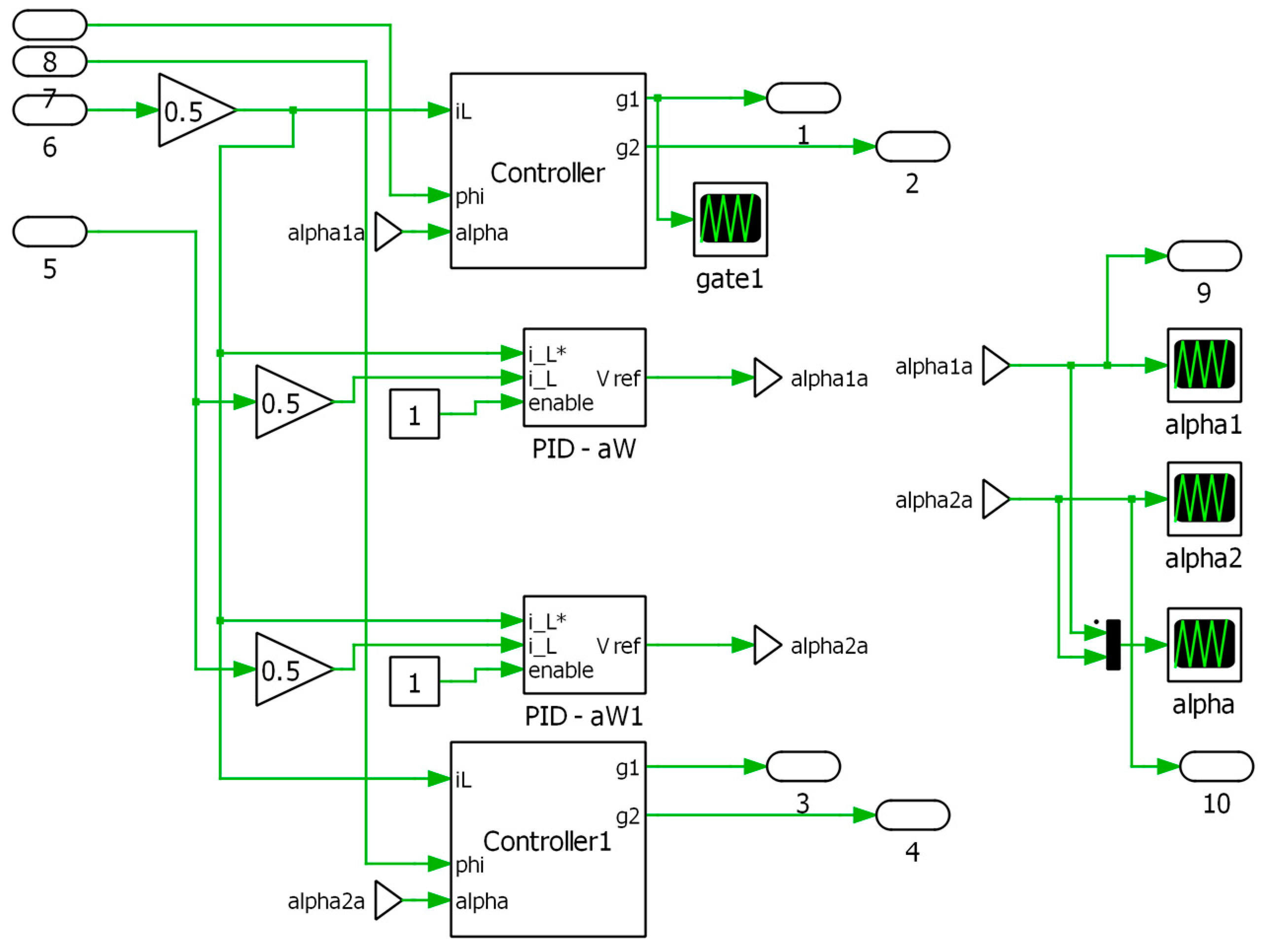
The simulation results were carried out arranging cycloconverters in PLECS® tool. The global block scheme of the simulated circuit is reported in Figure 16. As in Figure 7, the rectangles in different colors show the simulated systems: in blue, the plasma filaments equivalent coils; in red, the divertor coils (DIV1, DIV2, DIV3); in green, the vertical stabilization coils (VSL, VSU). Figure 17 shows the cycloconverter topology simulation schematic for all of the DIV coils, composed of the four SCR rectifiers connected to operate as a 12-pulse cycloconverter supplied by two transformers with 30 degrees phase shifted secondaries. Figure 18 shows the control and command generation scheme for one single phase cycloconverter, made of two PID regulators with anti-wind-up output limitation and two command generators for the SCR rectifiers of the cycloconverter. The remaining systems were simulated as in the case of the inverter supplies, with ideal supplies, as described for Figure 7.
The voltages and currents of the VS coils and of the common mode inductance are not shown for this simulation, since they have basically the same behavior as those shown in Figure 9, Figure 10 and Figure 11.
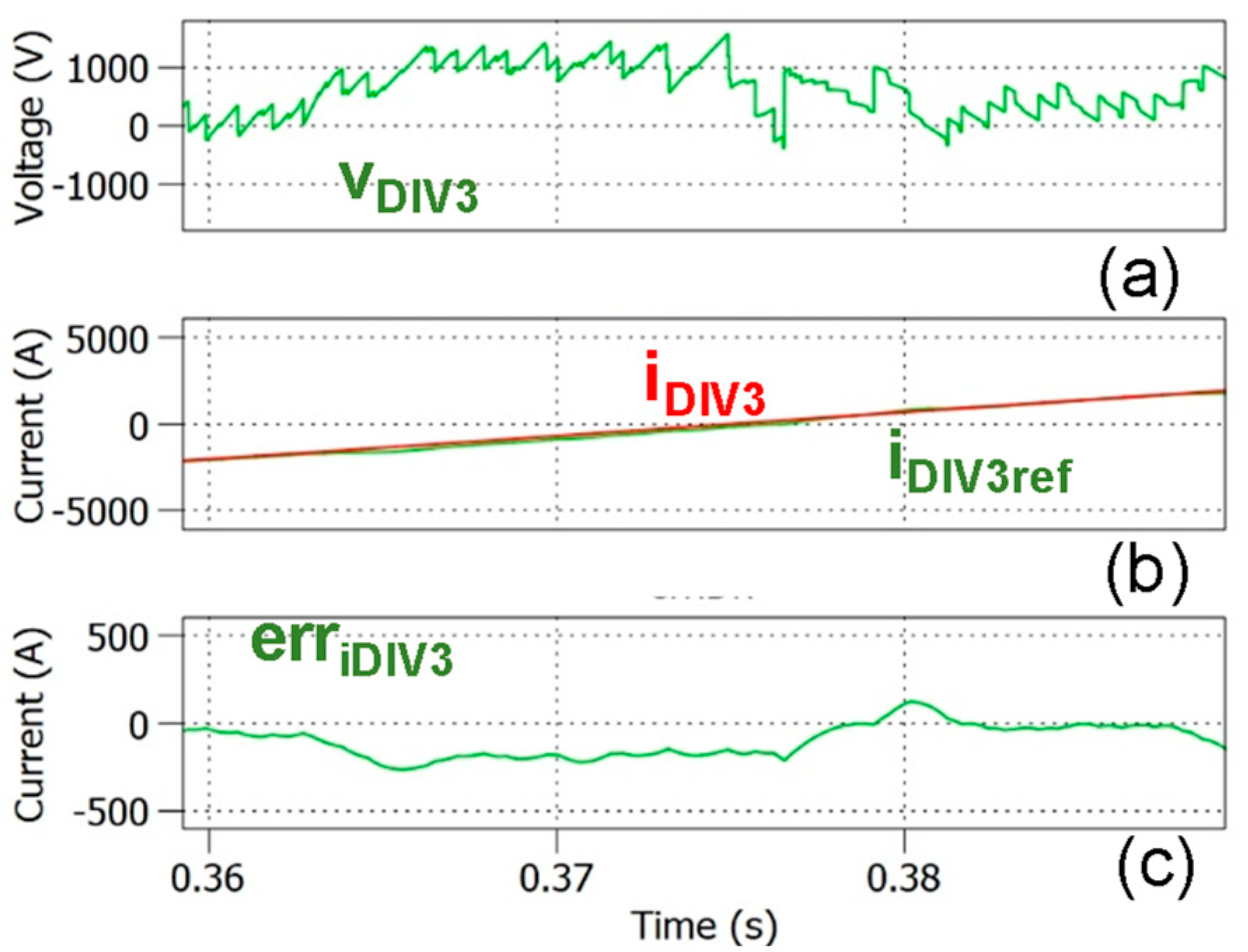
In Figure 19 the waveforms obtained for the DIV3 coil are displayed; the inverter voltage vDIV3 is shown (a); then the coil current iDIV3 and its reference iDIV3ref are shown (b); finally, the current error erriDIV3 is shown (c). Figure 20 shows one period (0.25 s) of the waveforms shown in Figure 19. Finally, Figure 21 displays a further detail of Figure 19 during one fundamental period of the VS coils (0.025 s).
The quantities for the three DIV coils are also shown: Figure 22 shows the output voltages of the single phase cycloconverters for DIV1, DIV2, DIV3 coils (vDIV1, vDIV2 and vDIV3).

4.3. Comparison of Electrical Simulation Results for IGBT-Based and SCR-Based Power Supplies

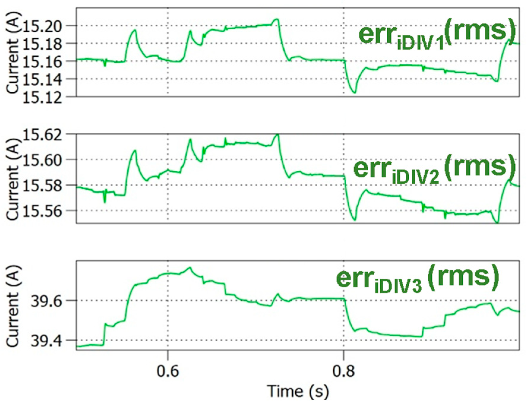
A comparison between the current errors obtained with IGBT-based inverters and single phase cycloconverter is made in Figure 23 and Figure 24.
As expected, the inverter yields prompter current control with rms current errors lower (roughly 20% of the values of Figure 24). This is due to the higher switching output frequency of the converter, obtained with the interleaved modulation strategy. The unfolder leg only commutates at the voltage reference sign changes; this means that its switching losses are neglectable, and the thermal design of the unfolder leg can be made reducing the number of components required; this is assessed in the thermal analysis section. The 12-pulse cycloconverter does not yield the same control promptness, as its average switching frequency is 12 times (600 Hz) the line frequency of 50 Hz. This brings values of the PID parameters of the current regulators that cannot be set as high as in the inverter’s case. Though, its use of mature, readily available high-current devices simplifies component selection.

5. Switches/Converters Thermal Analysis

An electro-thermal simulation of the two proposed solutions was performed in PLECS to evaluate the suitability of the selected power components.

5.1. IGBT-Based Inverter Electro-Thermal Simulation Results

This section focuses on the first solution, which consists of parallel-connected switching legs and a dedicated unfolding leg.
The four switching legs consist of four Infineon FF1800R23IE7 [27] IGBT half-bridge power modules, with a breakdown voltage of 2300 V. Each IGBT has a continuous current rating of 1800 A at a case temperature (Tcase) of 85 °C. The unfolding leg uses the same modules but is parallel connected for a total of three modules connected in parallel. The direct parallel operation is possible due to the extremely low switching frequency of the unfolding leg; therefore, uneven commutation losses will not significantly impact the overall losses. Additionally, these IGBTs feature a positive temperature coefficient of conduction. This characteristic promotes natural current balancing among the parallel devices: if one device begins to overheat, its conduction resistance increases, thereby reducing its current share and helping to redistribute both conduction and switching losses more evenly across all modules.
The implemented electro-thermal model is shown in Figure 25. Specifically, Figure 25a shows the model developed for one of the four switching legs, where the electro-thermal model of the FF1800R23IE7 IGBT was provided by the manufacturer. Each power module is mounted on an individual liquid-cooled heatsink. According to the datasheet, the baseplate surface area of the FF1800R23IE7 module is 0.021242 m2. Assuming a high-performance liquid-cooled heatsink with a thermal resistance per unit area of 0.0002 K·m2/W, the resulting thermal resistance between heatsink and coolant (Rth,hs-cl) is approximately 0.0094 K/W (as depicted in Figure 25a).
The value of 0.0002 K·m2/W used in the electro-thermal model is the assumed area-normalized thermal resistance R″ (i.e., the inverse of a convective heat-transfer coefficient). This corresponds to a heat-transfer coefficient h = 1/R″ = 5000 W/m2·K, a value representative of high-performance liquid-cooled cold-plate or micro-channel designs operating in turbulent flow with minimal interface resistance. The literature on localized cold-plate designs reports effective heat-transfer coefficients between 7000 and 27,000 W/m2·K under moderate to high flow rates, confirming that the selected value is reasonable and practically achievable [28,29,30,31]. In addition, a liquid-cooled heatsink specifically developed for the same module package was experimentally demonstrated in [32], achieving an even lower overall thermal resistance of 0.0072 K/W without extensive optimization, further supporting the validity of the assumption. Finally, a coolant inlet temperature of 50 °C is assumed in the analysis.
Similarly, Figure 25b shows the implemented electro-thermal model for the modules used in the unfolding leg (only one module is analyzed, as the thermal behavior of the others is the same).
Simulation results are reported in Figure 26. The top plot shows both the reference and measured current in the DIV1 coil. The middle plot displays the junction temperatures of the semiconductors in one of the switching legs, while the bottom plot shows those of the unfolding leg.
From the temperature profile of the switching leg, it can be observed that when the current in the DIV coil is negative (i.e., entering the switching node), losses are primarily distributed between the low-side IGBT and the high-side antiparallel diode. Conversely, when the current is positive (i.e., exiting the switching node), losses shift to the high-side IGBT and the low-side antiparallel diode. The maximum junction temperature reached by the switching leg’s semiconductors is 145 °C, which remains below both the recommended operating limit of 150 °C and the absolute maximum rating of 175 °C.
The bottom plot in Figure 26 shows the junction temperature of the unfolding leg semiconductors. As the switching frequency is low, the majority of losses stem from conduction rather than switching. Following a similar pattern as the switching leg, when the current in the DIV coil is negative (exiting the switching node via the unfolding leg), the high-side IGBT and low-side diode conduct, depending on the reference voltage. When the current is positive (entering the switching node), conduction involves the low-side IGBT and the high-side diode. The highest junction temperature observed for the low-side IGBT in the unfolding leg is below 130 °C, which is within the 150 °C recommended limit and well below the 175 °C absolute maximum rating. It is important to note that during these tests, the current amplitude was 5500 A, corresponding to the maximum expected load for the system, while during normal operative conditions, lower currents are generally expected. In both cases the semiconductors are fully exploited; however, if required, it may be possible to add an additional safety margin by increasing the number of the switching legs (assuming use of the same power module) and the number of modules connected in parallel for the unfolding leg.

5.2. SCR-Based Cycloconverter Electro-Thermal Simulation Results

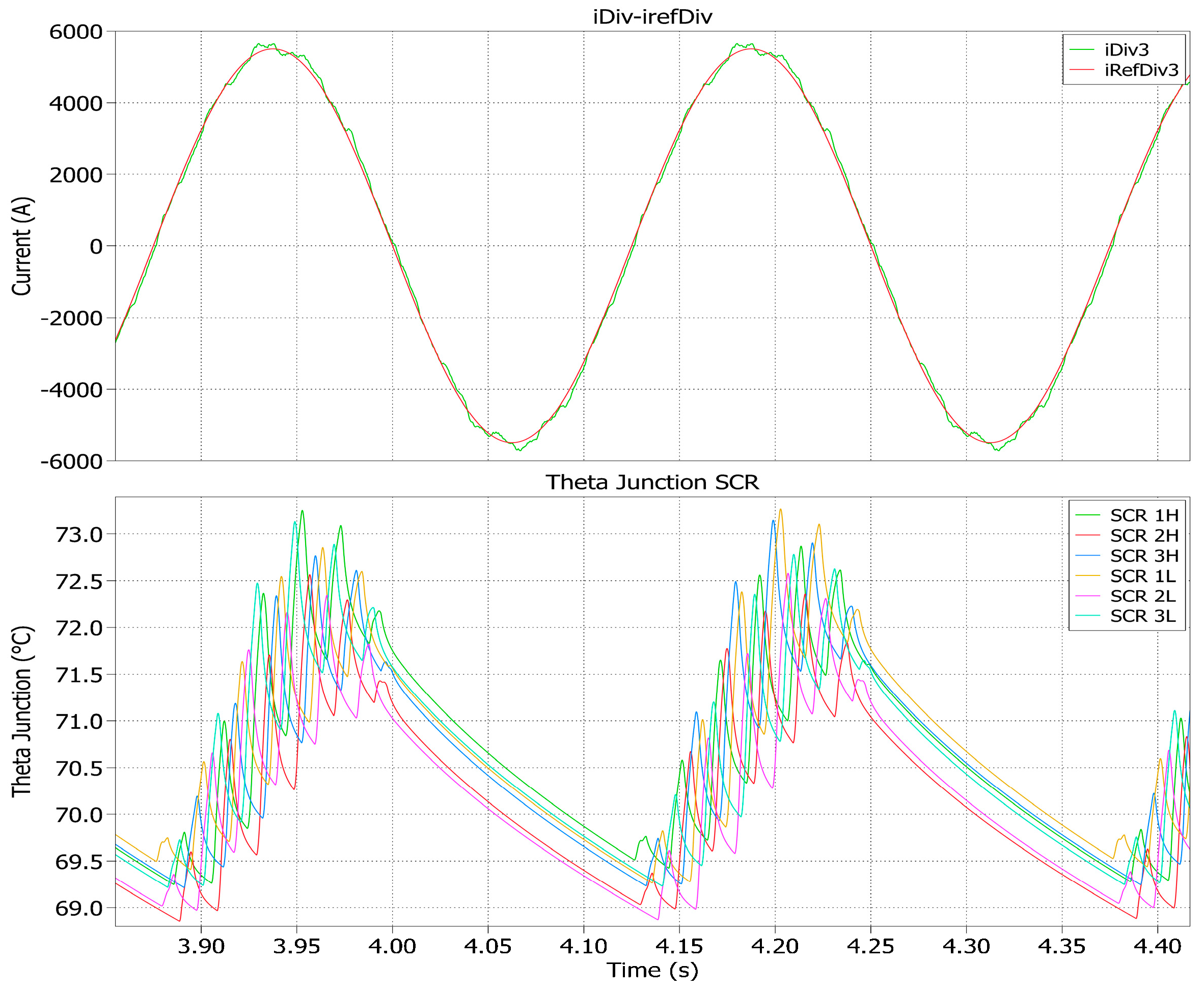
A similar analysis was carried out for the SCR-based cycloconverter solution, which uses T4771N22TOF SCR manufactured by Infineon [27]. This device has a breakdown voltage of 2200 V and a rated average current of 5290 A at a case temperature (Tcase) of 70 °C. The corresponding electro-thermal model is shown in Figure 27, where one of the converter bridges has been analyzed. As in the previous case, a coolant temperature of 50 °C was assumed. The component models were derived from datasheet data, and each SCR was assumed to be mounted on a double-sided liquid-cooled heatsink, as recommended by the manufacturer. Assuming a heatsink with a thermal resistance per unit area of 0.001 K·m2/W (i.e., five times higher than the previous case, considering the older technology), the resulting thermal resistance between heatsink and coolant (Rth,hs-cl), considering a surface for each SCR of 0.0157 m2, is 0.063 K/W. This cooling setup is included in the thermal model of the devices. The simulation results are reported in Figure 28. The top plot shows both the reference and the measured current in the DIV coil, while the bottom plot illustrates the junction temperatures of the six SCRs within the analyzed bridge. It should be noted that the bridge under analysis conducts only when the current in the coil is positive, and when the current is negative, conduction is handled by the complementary bridge. In this scenario, the maximum junction temperature remains below 75 °C, which is well within the device’s recommended operating range and significantly below its maximum allowable junction temperature of 125 °C.

6. Discussion

The thermal analysis of both solutions demonstrated that they are feasible from an implementation standpoint. However, the first solution, based on IGBT modules, is more critical from a thermal point of view and may require additional switches in parallel for the switching leg, as well as higher-current devices for the unfolding leg, if greater safety margins are required. In contrast, the SCR-based solution exhibits a more comfortable thermal margin under the same operating conditions.
Furthermore, the second solution offers a significantly higher tolerance to impulsive currents, with a peak withstand capability of up to 91 kA before device failure. An additional advantage of the SCR-based topology is that it does not require a front-end rectifier and can operate directly from the AC grid. However, this approach necessitates the use of appropriately phase-shifted transformers, which introduces an added level of system complexity. Another key benefit of the SCR-based approach is the greater maturity and availability of components, especially in the high-current range. Multiple commercially available SCRs can handle the required current levels, whereas only a limited number of IGBT solutions meet these demands, often necessitating the parallelization of multiple devices. The main drawback of the SCR-based solution lies in its limited dynamic performance. Due to its inherently low switching frequency, it is not suitable for achieving high-bandwidth current regulation, which restricts the performance of the PI current controller.
The comparison between the two solutions is summarized in Table 2.

7. Conclusions

A study was conducted to evaluate two converter topologies to supply the Tokamak Divertor Coils (DIV): one based on IGBT modules and the other on SCRs.
The results demonstrate that both solutions are feasible from the control and thermal points of view, under the expected operating conditions, with semiconductors operating within safe temperature limits. The IGBT-based solution, while viable, is thermally more constrained and may require additional parallel devices in the switching leg and higher-current-rated components in the unfolding leg to ensure sufficient safety margins. Nevertheless, it offers superior dynamic performance and is better suited in case the physical analysis of plasma behavior would show that a fast current regulation would be required due to its higher switching frequency. Conversely, the SCR-based solution benefits from a wider thermal margin, higher impulse current capability (up to 91 kA), and direct AC grid compatibility without a front-end rectifier. Its use of mature, readily available high-current devices also simplifies component selection. However, the need for phase-shifted transformers adds system complexity, and the inherently low switching frequency limits the achievable bandwidth of the current control loop. Ultimately, the choice between the two topologies should be guided by the tokamak application requirements, balancing thermal robustness, control performance, and system complexity. The engineering implementation challenges of the two schemes, such as considerations for installation and maintenance, have not been addressed at this stage of the work: they will regard future developments of the work.

Author Contributions

Conceptualization, G.G., S.M., R.B., F.S. and A.L.; methodology, G.G., S.M., R.B., F.S. and A.L.; software, G.G., S.M., R.B., F.S. and A.L.; formal analysis, G.G., S.M., R.B., F.S. and A.L.; writing—original draft preparation, G.G., S.M., R.B., F.S. and A.L.; writing—review and editing, G.G., S.M., R.B., F.S. and A.L.; visualization, G.G., S.M., R.B., F.S. and A.L.; supervision, G.G., S.M., R.B., F.S. and A.L. All authors have read and agreed to the published version of the manuscript.

Funding

This research received no external funding.

Institutional Review Board Statement

Not applicable.

Informed Consent Statement

Not applicable.

Data Availability Statement

The original contributions presented in this study are included in the article. Further in-quiries can be directed to the corresponding author.

Conflicts of Interest

The authors declare no conflict of interest.

References

  1. EUROfusion. European Research Roadmap to the Realisation of Fusion Energy. 2018. Available online: http://www.euro-fusion.org/eurofusion/roadmap/ (accessed on 30 August 2025).
  2. ITER Website. Available online: http://www.iter.org (accessed on 30 August 2025).
  3. Fusion Industry Association. Available online: https://www.fusionindustryassociation.org/ (accessed on 30 August 2025).
  4. Federici, G.; Bachmann, C.; Barucca, L.; Baylard, C.; Biel, W.; Boccaccini, L.V.; Bustreo, C.; Ciattaglia, S.; Cismondi, F.; Corato, V.; et al. Overview of the DEMO staged design approach in Europe. Nucl. Fusion 2019, 59, 066013. [Google Scholar] [CrossRef]
  5. Siccinio, M.; Biel, W.; Cavedon, M.; Fable, E.; Federici, G.; Janky, F.; Lux, H.; Maviglia, F.; Morris, J.; Palermo, F.; et al. DEMO physics challenges beyond ITER. Fusion Eng. Des. 2020, 156, 1116033. [Google Scholar] [CrossRef]
  6. Wesson, J. Tokamaks, 3rd ed.; Clarendon Press: Oxford, UK, 2003. [Google Scholar]
  7. Lampasi, A.; Pipolo, S.; Albanese, R.; Ambrosino, R.; Bifaretti, S.; Bojoi, R.; Bonaiuto, V.; Castaldo, A.; Caldora, M.; Cocchi, A.; et al. Overview of the Divertor Tokamak Test (DTT) coil power supplies. Fusion Eng. Des. 2023, 188, 113442. [Google Scholar] [CrossRef]
  8. Martone, R.; Albanese, R.; Crisanti, F.; Martin, P.; Pizzuto, A. DTT Divertor Tokamak Test facility—Interim Design Report, ENEA, 2019. Available online: https://iris.unibas.it/bitstream/11563/136383/2/DTT_IDR_2019_WEB1.pdf (accessed on 15 July 2025).
  9. Romanelli, F. Divertor Tokamak Test facility Project: Status of Design and Implementation. Nucl. Fusion 2024, 64, 112015. [Google Scholar] [CrossRef]
  10. Kotschenreuther, M.; Valanju, P.M.; Mahajan, S.M.; Wiley, J.C. On heat loading, novel divertors, and fusion reactors. Phys. Plasmas 2007, 14, 072502. [Google Scholar] [CrossRef]
  11. Ambrosino, R. DTT—Divertor Tokamak Test facility: A testbed for DEMO. Fusion Eng. Des. 2021, 167, 1123300. [Google Scholar] [CrossRef]
  12. Innocente, P.; Ambrosino, R.; Brezinsek, S.; Calabrò, G.; Castaldo, A.; Crisanti, F.; Dose, G.; Neu, R.; Roccella, S. Design of a multi-configurations divertor for the DTT facility. Nucl. Mater. Energy 2022, 33, 101276. [Google Scholar] [CrossRef]
  13. Acampora, E.; Ambrosino, R.; Castaldo, A.; Iervolino, R. Magnetic control of DTT alternative plasma configurations. Fusion Eng. Des. 2023, 192, 113617. [Google Scholar] [CrossRef]
  14. Griva, G.; Musumeci, S.; Stella, F.; Bojoi, R.; Lampasi, A.; Zito, P.; Bifaretti, S. HIL Investigation of a Single-Phase Inverter for a Tokamak Non-Axisymmetric In-Vessel Coil Power Supply. IEEE Trans. Ind. Appl. 2024, 60, 4076–4086. [Google Scholar] [CrossRef]
  15. Griva, G.; Musumeci, S.; Stella, F.; Bojoi, R.; Lampasi, A.; Bifaretti, S. C-HIL Implementation of Cascaded Multilevel Inverter for Vertical Stabilization and Radial Control Power Supplies of Divertor Tokamak Test. In Proceedings of the 2024 International Conference on Smart Energy Systems and Technologies (SEST), Torino, Italy, 10–12 September 2024; pp. 1–6. [Google Scholar]
  16. Lampasi, A.; Testa, R.; Gudala, B.; Terlizzi, C.; Pipolo, S.; Tenconi, S. Optimization of DC Energy Storage in Tokamak Poloidal Coils. Appl. Sci. 2024, 14, 8975. [Google Scholar] [CrossRef]
  17. Acampora, E.; Albanese, R.; Ambrosino, R.; Castaldo, A.; Innocente, P.; Loschiavo, V.P. Conceptual design of in-vessel divertor coils in DTT. Fusion Eng. Des. 2023, 193, 113651. [Google Scholar] [CrossRef]
  18. Ambrosino, R.; Ariola, M.; Bachmann, C.; Castaldo, A.; Maviglia, F.; Mattei, M.; Tartaglione, G. Sweeping control performance on DEMO device. Fusion Eng. Des. 2021, 197, 114029. [Google Scholar] [CrossRef]
  19. Teschke, M.; ASDEX Upgrade Team. Development of an active overvoltage protection for the new ASDEX upgrade divertor coils. Fusion Eng. Des. 2021, 171, 112541. [Google Scholar] [CrossRef]
  20. Syah, M.N.; Firmansyah, E.; Utomo, D.R. Interleaved Bidirectional DC-DC Converter Operation Strategies and Problem Challenges: An Overview. In Proceedings of the IEEE International Conference in Power Engineering Application (ICPEA), Shah Alam, Malaysia, 7–8 March 2022; pp. 1–6. [Google Scholar] [CrossRef]
  21. Galkin, I.A.; Saltanovs, R.; Bubovich, A.; Blinov, A.; Peftitsis, D. Considerations on Combining Unfolding Inverters with Partial Power Regulators in Battery–Grid Interface Converters. Energies 2023, 17, 893. [Google Scholar] [CrossRef]
  22. Do, T.A.; Nguyen, Q.D.; Vu, P.; Ngo, M.D.; Ahn, S. Comparative Analysis of PWM Techniques for Interleaved Full Bridge Converter in an AC Battery Application. Energies 2023, 17, 375. [Google Scholar] [CrossRef]
  23. Datasheet URL IGBT Module FF1800R23IE7. Available online: https://www.infineon.com/assets/row/public/documents/non-assigned/49/infineon-ff1800r23ie7-datasheet-en.pdf (accessed on 15 July 2025).
  24. Wu, B.; Pontt, J.; Rodríguez, J.; Bernet, S.; Kouro, S. Current-Source Converter and Cycloconverter Topologies for Industrial Medium-Voltage Drives. IEEE Trans. Ind. Electron. 2008, 55, 2786–2797. [Google Scholar] [CrossRef]
  25. Tahmid, M.R.; Malek, M.A.; Islam, M.R.; Khan, M.A.G. Advanced thyristor-based cycloconverter for efficient three-phase conversion with low THD. E-Prime—Adv. Electr. Eng. Electron. Energy 2025, 11, 100918. [Google Scholar] [CrossRef]
  26. Barría, V.G.; Olivares, J.P. Design of a 12-pulse cycloconverter with fault-tolerance capability. In Proceedings of the 2011 14th European Conference on Power Electronics and Applications, Birmingham, UK, 30 August–1 September 2011; pp. 1–10. [Google Scholar]
  27. Datasheet URL SCR T4771N22TOF. Available online: https://www.infineon.com/assets/row/public/documents/60/49/infineon-t4771n-ds-en-de.pdf (accessed on 15 July 2025).
  28. Kandlikar, S.G.; Hayner, C.N. Liquid Cooled Cold Plates for Industrial High-Power Electronic Devices—Thermal Design and Manufacturing Considerations. Heat Transf. Eng. 2009, 30, 918–930. [Google Scholar] [CrossRef]
  29. Aranzabal, I.; Perez-Peña, F.J.; Lima, A.V.; de la Osa, A.R.; Alonso, J.M. Comparison between conventional single-phase and two-phase cooling systems for electric vehicle IGBT modules. IEEE Trans. Power Electron. 2019, 34, 11236–11248. [Google Scholar] [CrossRef]
  30. Kandlikar, S.G. Liquid Cooled Cold Plates for Industrial High-Power Electronic Devices: A Review. Heat Transf. Eng. 2010, 31, 156–171. [Google Scholar]
  31. Price, A.; Savulak, M. A review of selected thermal management solutions for avionics. IEEE Trans. Components Packag. Technol. 2003, 26, 26–39. [Google Scholar] [CrossRef]
  32. Akgül, M.B.; Erçel, F.S. Thermal Performance Analysis of a Liquid Cooling Plate for Power Electronics. Celal Bayar Üniversitesi Fen Bilimleri Dergisi 2021, 20, 72–81. [Google Scholar] [CrossRef]
Figure 1. Arrangement of the DTT in-vessel coils: VS (2 coils, in gray), DIV (4 coils in the original solution, 3 coils in the actual operation conditions, in red) and NA (3 × 9 = 27 coils, in violet).
Applsci 15 10441 g001
Figure 2. Configuration of the three DIV coils with respect to the DTT vacuum vessel. (a) 3D view. (b) Cross−section.
Applsci 15 10441 g002
Figure 3. Full-Bridge DC–AC power converter IGBT-based power supply solution for the DIV coils.
Applsci 15 10441 g003
Figure 4. Full-Bridge DC–AC power converter IGBT-based with the interleaved solution and unfolder switch.
Applsci 15 10441 g004
Figure 5. (a) Modulation voltage (Vmod), with a PWM signal VPWM and the unfolder signal command (VUF) waveforms. (b) Zoomed view focusing on the PWM signal. (c) Switching leg with the modulation strategy circuit.
Applsci 15 10441 g005
Figure 6. (a) 12-pulse cycloconverter topology; (b) 6-pulse SCR cycloconverter; (c) 12-pulse cycloconverter output voltage example for positive half-wave.
Applsci 15 10441 g006
Figure 7. Block schematic of the global supply system for the DIV coils (red rectangles) used in PLECS® simulations.
Applsci 15 10441 g007
Figure 8. Scheme of single−phase inverter with an interleaved switching pole and unfolder switching leg used in PLECS® simulations.
Applsci 15 10441 g008
Figure 9. VS coils and common mode inductance: (a) output voltages of the single−phase inverters for VS coils (vDM) and common mode inductance (vCM); (b) differential mode current reference iDMref and VS coils currents iVSU, iVSL; (c) common mode current reference iCMref and common mode inductance current iLIM.
Applsci 15 10441 g009
Figure 10. VS coils and common mode inductance during one period (0.25 s) of the DIV coils currents: (a) output voltages of the single−phase inverters for VS coils (vDM) and common mode inductance (vCM); (b) differential mode current reference iDMref and VS coils currents iVSU, iVSL; (c) common mode current reference iCMref and common mode inductance current iLIM.
Applsci 15 10441 g010
Figure 11. VS coils and common mode inductance during one period (0.025 s) of the VS coils currents: (a) output voltages of the single−phase inverters for VS coils (vDM) and common mode inductance (vCM); (b) differential mode current reference iDMref and VS coils currents iVSU, iVSL; (c) common mode current reference iCMref and common mode inductance current iLIM.
Applsci 15 10441 g011
Figure 12. DIV3 coil: (a) output voltage of the single−phase inverter vDIV3; (b) coil current iDVI3 and current reference iDVI3ref; (c) coil current error erriDIV3.
Applsci 15 10441 g012
Figure 13. DIV3 coils during 1 fundamental period (0.25 s): (a) output voltage of the single−phase inverter vDIV3; (b) coil current iDVI3 and current reference iDVI3ref; (c) coil current error erriDIV3.
Applsci 15 10441 g013
Figure 14. DIV3 coil during 1 fundamental period of the VS coils (0.025 s): (a) output voltage of the single−phase inverter vDIV3; (b) coil current iDVI3 and current reference iDVI3ref; (c) coil current error erriDIV3.
Applsci 15 10441 g014
Figure 15. DIV coils inverter voltages vDIV1, vDIV2, and vDIV3.
Applsci 15 10441 g015
Figure 16. Block schematic of the global supply system for the DIV coils (red rectangles) used in PLECS® simulations.
Applsci 15 10441 g016
Figure 17. Scheme of single−phase cycloconverter used in PLECS® simulations.
Applsci 15 10441 g017
Figure 18. Control and command generation scheme for one single−phase cycloconverter used in PLECS® simulations.
Applsci 15 10441 g018
Figure 19. DIV3 coil: (a) output voltage of the single−phase cycloconverter vDIV3; (b) coil current iDIV3 and current reference iDIV3ref; (c) coil current error erriDIV3.
Applsci 15 10441 g019
Figure 20. DIV3 coil during 1 fundamental period (0.25 s): (a) output voltage of the single−phase cycloconverter vDIV3; (b) coil current iDIV3 and current reference iDIV3ref; (c) coil current error erriDIV3.
Applsci 15 10441 g020
Figure 21. DIV3 coil during 1 fundamental period of the VS coils (0.025 s): (a) output voltage of the single−phase cycloconverter vDIV3; (b) coil current iDIV3 and current reference iDIV3ref; (c) coil current error erriDIV3.
Applsci 15 10441 g021
Figure 22. Output voltages of the single−phase cycloconverters for DIV1, DIV2, DIV3 coils vDIV1, vDIV2, and vDIV3.
Applsci 15 10441 g022
Figure 23. The rms values of the coil current errors for DIV1, DIV2, DIV3 coils supplied by IGBT-based inverters.
Applsci 15 10441 g023
Figure 24. The rms values of the coil current errors for DIV1, DIV2, DIV3 coils supplied by SCR-based cycloconverters.
Applsci 15 10441 g024
Figure 25. PLECS electro−thermal model. (a) Interleaving switching leg. (b) Unfolding leg.
Applsci 15 10441 g025
Figure 26. Electro−thermal simulation results during normal operating conditions. (Top plot): measured and reference current in the DIV1 coil. (Middle plot): junction temperature of power semiconductors of the interleaved switching leg. (Bottom plot): junction temperature of power semiconductors of the unfolding leg.
Applsci 15 10441 g026
Figure 27. PLECS electro−thermal model of one of the SCR bridges.
Applsci 15 10441 g027
Figure 28. Electro−thermal simulation results during normal operating conditions. (Top plot): measured and reference current in the DIV1 coil. (Bottom plot): junction temperature of the six SCRs of the bridge rectifier.
Applsci 15 10441 g028
Table 1. Main characteristics of one DC/AC IGBT-based inverter.
ParameterValue
Output voltage (peak max (DiV3)1.7 kV
Peak output current5.5 kA
IGBT rated voltage VCES 2300 V
IGBT rated current1800 A
Repetitive peak forward
Current (tp = 1 ms)
3600 A
Collector–emitter
Saturation voltage VCEsat @125 °C, Typ.
2.15 V
Diode forward voltage VF @125 °C, Typ.3 V
Diode peak reverse recovery
Current IRM @125 °C,
1450 A
Part number and package: FF1800R23IE7 by Infineon PrimePACK™3+ B-series module
Number of switching legs for the interleaved approach of one DC/AC unit4
Parallel switches for the unfolder low-side and high-side of one DC/AC unit3
Table 2. Comparison between IGBT-based and SCR-based power supplies.
ParameterIGBT InvertersSCR Cycloconverters
Current control error (RMS, for DIV3)39.6 A135 A
Thermal margin (percentage of maximum junction temperature vs. limit)130 °C/150 °C
86.7%
73 °C/125 °C
58.4%
Estimated number of main switching devices14 IGBTs + 14 diodes24 SCRs
Disclaimer/Publisher’s Note: The statements, opinions and data contained in all publications are solely those of the individual author(s) and contributor(s) and not of MDPI and/or the editor(s). MDPI and/or the editor(s) disclaim responsibility for any injury to people or property resulting from any ideas, methods, instructions or products referred to in the content.