Article

Comparative Method Between Eddy Current and Optical Microscopy in the Determination of Thickness of 6063 Aluminum Alloy Anodization

by
Jose Cabral-Miramontes
1,*,
Citlalli Gaona-Tiburcio
1,
Erick Maldonado-Bandala
2,
Daniel Vera Cervantes
1,
Demetrio Nieves-Mendoza
2,
Ce Tochtli Mendez-Ramirez
2,
Maria Lara-Banda
1,
Miguel Angel Baltazar-Zamora
2,
Javier Olguin-Coca
3 and
Facundo Almeraya-Calderon
1,*
1
Universidad Autónoma de Nuevo León, FIME, Centro de Investigación e Innovación en Ingeniería Aeronáutica (CIIIA), San Nicolás de los Garza 66455, Mexico
2
Facultad de Ingeniería Civil, Universidad Veracruzana, Xalapa 91000, Mexico
3
Área Académica de Ingeniería y Arquitectura, Universidad Autónoma del Estado de Hidalgo, Carretera Pachuca-Tulancingo Km. 4.5, Pachuca 42082, Mexico
*
Authors to whom correspondence should be addressed.
Appl. Sci. 2025, 15(16), 9025; https://doi.org/10.3390/app15169025
Submission received: 9 July 2025 / Revised: 29 July 2025 / Accepted: 13 August 2025 / Published: 15 August 2025
(This article belongs to the Special Issue Corrosion and Protection with Hard Coatings)

Abstract

This study compares the Eddy current technique and optical microscopy for measuring the anodized layer thickness in a 6063 aluminum alloy with the aim of establishing an efficient and accurate methodology capable of delivering optimal results in a time-efficient manner. Optical microscopy was used as the reference method, with five measurements taken in different fields for each specimen. The Eddy current method was applied using two calibration strategies: one calibration before each measurement and another after every ten specimens. The Bland–Altman analysis was employed to compare both measurement techniques. The results indicated that the calibration before each measurement strategy using Eddy current showed higher agreement with the reference method, suggesting that both techniques can be considered equivalent and interchangeable. Furthermore, the Eddy current method demonstrated significant advantages in detecting thickness variations along the specimen, revealing non-uniform distribution of the anodized layer. This method also proved to be faster and eliminated the need for metallographic preparation required by optical microscopy, thus significantly reducing analysis time and cost. In conclusion, the Eddy current method with calibration before each measurement strategy is proposed as an effective alternative for measuring anodized layer thickness in applications where speed and precision are critical.

1. Introduction

Aluminum is widely used in various industries due to its low weight, high corrosion resistance, good thermal and electrical conductivity and ease of machining and recycling. However, in its pure form, it has limited mechanical strength, restricting its use in more demanding applications. To improve these properties, aluminum is alloyed with elements such as copper, manganese, magnesium, silicon and zinc, which enhance its strength through deformation processes or heat treatments. Among these, the 6063 aluminum alloy is one of the most used due to its good response to heat treatment and quenching. Its main strengthening mechanism involves the formation of magnesium silicide (Mg2Si) precipitates, which provide excellent strength, ductility and hardness [1,2].
Aluminum and its alloys possess inherent protection provided by a natural oxide layer that is formed when they are exposed to air. However, this natural oxide layer (Al2O3) is thin and heterogeneous, making it insufficient to offer adequate protection against aggressive environments [3]. Therefore, the anodization process is an essential electrolytic method in the aluminum industry, playing a crucial role in protecting and enhancing the properties of this metal. Through this process, an oxide layer is formed on the surface of aluminum, providing increased resistance to corrosion, abrasion and other adverse atmospheric agents. This layer, which can be either transparent or colored, offers considerable versatility in its applications [4,5,6]. The determination of the anodized layer thickness is highly relevant, as it represents a quantitative parameter that enables comparison between different anodization processes, which may be influenced by different variables. Furthermore, the thickness of this layer is directly related to fundamental material properties, such as corrosion resistance, wear resistance and the ease of surface cleaning of aluminum [5].
There are various methods available to determine the thickness of the anodized layer, which differ depending on the purpose of the anodization process or the nature of the part being treated. One of the most used methods for determining the thickness of the anodized layer is optical microscopy. This method involves measuring the thickness on the cross-section of a sample prepared in accordance with ASTM B487-85 [7], which specifies the standard methodology for this type of measurement. However, optical microscopy has certain limitations, particularly in the depth of field. As the magnification of the objective increases, image resolution decreases, making it difficult to distinguish two adjacent points as separate units at magnifications of 1500× or higher [8,9]. The Eddy current method allows for non-contact measurement of the anodized layer thickness without sample preparation. It operates based on electromagnetic induction: an alternating current passed through a coil generates a magnetic field that induces circulating currents (Eddy currents) on the surface of a conductive material. These currents produce a secondary magnetic field that alters the coil’s impedance. As the coating thickness increases, the amplitude of the induced currents decreases, enabling a correlation between signal variations and coating thickness for accurate, efficient measurement [10]. A diagram showing how Eddy currents are generated in a non-magnetic and non-conductive coating is presented in Figure 1.
X-ray fluorescence spectroscopy (XRF) is the most widely used technique in industry for thickness measurement and quality control, as it does not require sample preparation and provides rapid and accurate analysis of material quality [11]. With this XRF technique, thickness can be extrapolated from the data using standards [12], employing analytical equations from the fundamental parameter method (FP) [13] or through Monte Carlo (MC) simulations [14,15,16]. Other non-destructive techniques commonly used for research purposes are ellipsometry [17] (rarely used in metal coatings); X-ray reflectivity (XRR) [18,19], capable of detecting thicknesses ranging from tens of nanometers to a few micrometers; electron probe microanalysis (EPMA) [20,21], commonly used for quantitative purposes; and X-ray photoemission spectroscopy (XPS), which can be used to determine thickness information down to the atomic scale [22,23,24].
The comparison of measurement methods is a fundamental procedure in the validation and improvement of analytical techniques, as it allows for the assessment of a new method’s performance relative to a previously established reference method. The reference method is considered a reliable and effective technique, serving as a benchmark to determine the accuracy and precision of the method under evaluation [25,26]. There are several approaches to comparing measurement methods, and one of the most widely used is the Bland–Altman method. Proposed by Martin Bland and Douglas G. Altman in 1983, this graphical technique is used to compare two measurement methods applied to the same variable, with the aim of evaluating whether there is a sufficient level of agreement to consider them interchangeable. In the Bland–Altman plot, the horizontal axis (x) represents the average of the two measurements, while the vertical axis (y) shows the difference between them [25,27]. To properly understand a Bland–Altman plot, it is essential to identify its main components, which consist of three horizontal lines: the bias, representing the mean of the differences; the upper limit of agreement; and the lower limit of agreement. The position of the data points relative to these lines allows for the evaluation of whether a new measurement method demonstrates acceptable agreement compared to an established method, and therefore, whether it can be considered a potential substitute [25]. Bias is the mean of the differences, and it is a key indicator in agreement analysis, as it quantifies the degree of similarity between the two measurement methods being evaluated. This value reflects, on average, how much the new method deviates from the reference method.
The limits of agreement are used to assess the accuracy and reliability of the new measurement method in comparison with a reference method. These limits are calculated under the assumption that the differences between both methods are normally distributed and define the range within which approximately 95% of the individual differences between measurements on the same subjects are expected to fall. Although early approaches referred to the empirical rule (±2 standard deviations), the more precise and statistically grounded approach uses the coefficient of repeatability, calculated as the mean of the differences ±1.96 times the standard deviation [25,28].
The relevance of this research lies in improving the measurement process of anodized layer thickness. Although the traditional optical microscopy method is precise, it involves high costs and long turnaround times for results. In this context, Eddy current has been identified as a promising alternative due to its ability to perform rapid, non-destructive measurements. However, the scientific literature lacks a direct and detailed comparison between Eddy current and optical microscopy in the context of anodized layer thickness determination, which justifies the need for this study. This research aims to compare both methods and optimize the calibration of the Eddy current technique to assess its applicability and advantages over optical microscopy. The objective is to enhance efficiency and accuracy while reducing the associated costs and processing time.

2. Materials and Methods

2.1. Materials

The test material selected was a 6063 aeronautical aluminum alloy bar onto which the anodization process was applied. The chemical composition obtained via X-ray fluorescence (Olympus DELTA XRF, Olympus, Houston, TX, USA) of aluminum 6063 is presented in Table 1. As can be seen, the chemical composition corresponds to a nominal aluminum alloy 6063.

2.2. Anodization Process

A total of 31 test specimens were anodized, varying the current density between 1.27 and 3.84 A/dm2, the electrolyte concentration between 180 and 407 g/L of sulfuric acid and the anodization time between 10 and 30 min. Prior to the anodization process, the specimens were subjected to cleaning and pickling treatment. Table 2 shows the different anodization process conditions for the 31 samples [29,30,31].

2.3. Optical Microscopy

For the optical microscopy measurement, the 6063 aluminum alloy samples were embedded in epoxy resin to facilitate handling and subsequently polished in accordance with ASTM E3 standards [32]. The sample preparation process for optical microscopy involved the use of epoxy resin. The polishing process was carried out using silicon carbide abrasive papers with grit sizes from 120 to 4000. A final fine polishing step was performed using diamond paste with a particle size of 1 μm.
The Zeiss Axio Observer 7 Materials microscope was used to measure the thickness of the anodized layer by means of optical microscopy (OM, Olympus, Hamburg, Germany), with 500× magnification being employed, following the guidelines established in ASTM B487-85 [7]. Five measurements were taken in two different fields for each specimen, resulting in a total of ten measurements.

2.4. Eddy Current

To measure the anodized layer thickness using Eddy current, an Elcometer 456T (Elcometer, Houston, TX, USA) device was used, equipped with a straight FNF probe. This device features a probe range from 0 to 1500 μm, with an accuracy of ±2.5 μm [33]. Ten measurements were taken on each side of the specimen, resulting in a total of twenty measurements per specimen. Based on these values, the average thickness of each specimen was calculated.
The thickness measurements using Eddy current were performed using two distinct methods: (1) calibrating the device after measuring each individual specimen and (2) calibrating the device after measuring the thickness of ten specimens. This approach was adopted to provide a wider variety of results, allowing for a more precise development of the methodology outlined in the general objective. The calibration of the Eddy current equipment before measurement of each sample and every ten samples was performed because the purpose of the research was to establish an efficient and accurate methodology capable of delivering optimal results in a timely manner. Each calibration of the Eddy current equipment takes around 3–4 min; therefore, this study verifies whether device calibration every ten samples provides accurate results in the measurements with respect to the reference measurement, which is optical microscopy.

3. Results and Discussion

3.1. Thickness Measurement Using Optical Microscopy

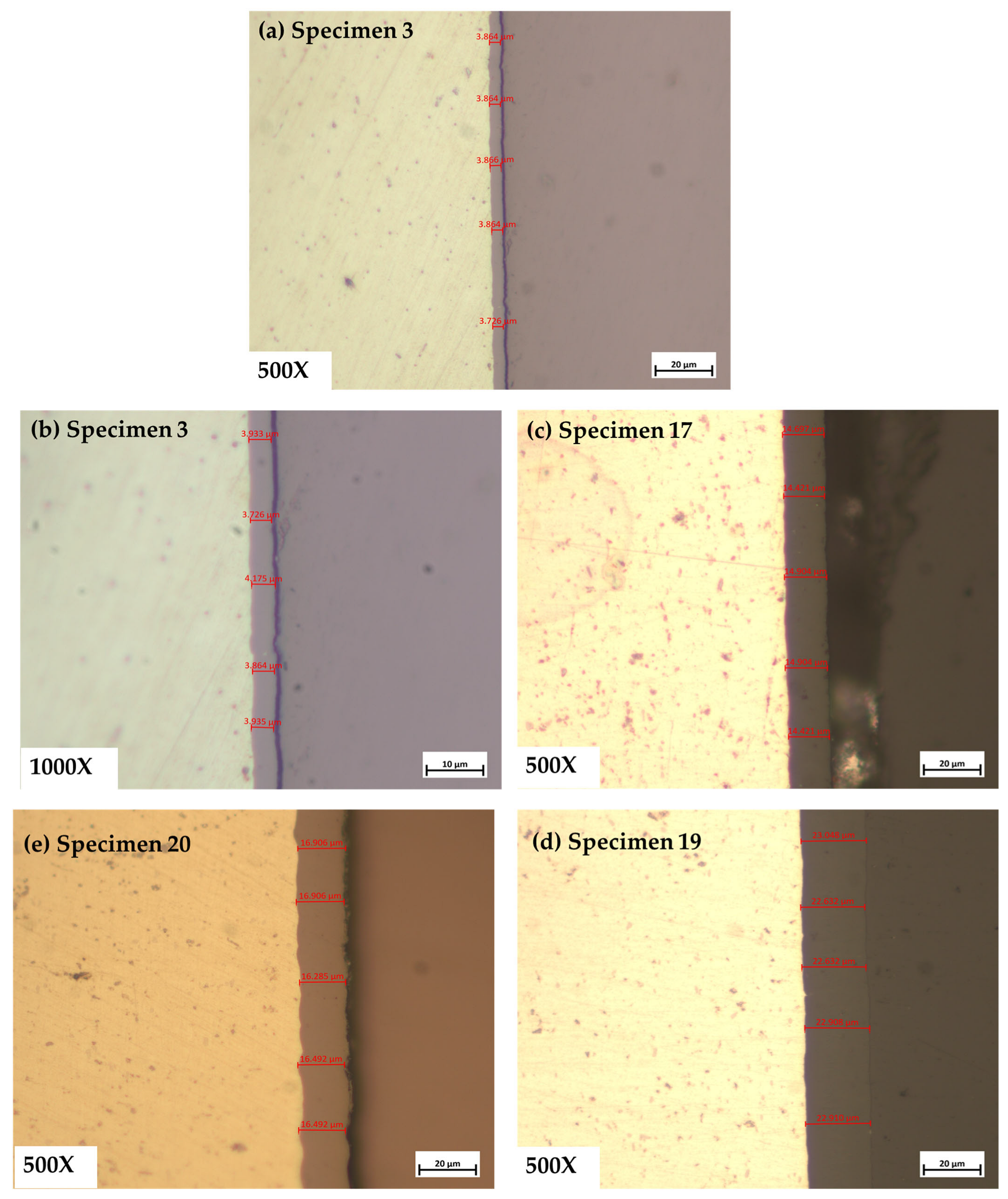
Some of the anodized layer thickness measurements obtained using the optical microscopy method are presented in Figure 2. It is important to note that this method only provides thickness values from a specific field of view, which does not represent the entire specimen. Therefore, the results may vary depending on the section of the specimen being analyzed.
Figure 2 shows the thickness of the anodized layer with different parameters, where Figure 2a,b corresponds to the sample with the lowest anodized thickness; Figure 2a has a magnification of 500×, and Figure 2b has a magnification of 1000×. This sample had an average thickness of 3.81 μm, and Figure 2e corresponds to the sample with the highest thickness, with an average of 22.76 μm.
The data obtained through optical microscopy were fundamental in establishing a benchmark for comparison with the results obtained using Eddy current. Measurements with this method were performed on only two cross-sections of each specimen, which limits the representativeness of the measurements, as they consider only a small portion of the specimen’s surface. It is important to note that the measurements were taken from the bottom part of the specimen, where the anodized layer exhibits greater uniformity. However, although optical microscopy provides precise measurements in the selected areas, it does not allow for the evaluation of the anodized layer thickness uniformity across the entire surface of the specimen without destroying other sections.
This limitation implies that a more comprehensive analysis would require taking multiple samples and performing additional cuts, which is both costly and impractical when evaluating many specimens.
An important observation that emerged during the measurements was the difference in results between optical microscopy and Eddy current testing. Initially, it was assumed that the thickness of the anodized layer was uniform throughout the specimen. However, the use of Eddy current revealed that this was not the case, showing significant variations in thickness across different areas of the specimen. This finding not only supports Eddy current testing as a more effective tool for determining thickness at multiple points on the part but also raises the possibility of investigating the causes of this variation in the anodization process [34]. It is possible that undetected factors may be affecting the uniformity of the process, thereby justifying the need for improved control over the anodization conditions [35].
In addition, optical microscopy presents certain limitations regarding the accuracy of measurements for very thin coatings. During the measurements, results corresponding to thicknesses below 5 μm were difficult to obtain accurately due to the resolution capacity at 500× magnification, which does not provide sufficient detail to clearly observe such small values [8,36]. In this context, obtaining more precise measurements for lower thicknesses would require the use of higher magnification, which could improve the accuracy of the results.

3.2. Thickness Measurement via Eddy Current

The average anodized layer thicknesses measured using optical microscopy and Eddy current testing are presented in Table 3.

3.2.1. Measurement with Calibration of Each Specimen

The anodized layer thicknesses measured using Eddy current testing with calibration performed before each specimen are shown in Figure 3. In this Figure, the specimens are listed in the order in which thickness measurements were taken. Additionally, it can be observed that most of the values obtained with this method are similar to those from optical microscopy, indicating a low percentage of measurement error.
The similarity observed between the results obtained through Eddy current and the optical microscopy reference values is mainly attributed to the calibration strategy implemented. By calibrating the Eddy current equipment before measuring each specimen, consistent precision is ensured for each reading. This method minimizes potential deviations that may occur during the measurement process. Furthermore, by avoiding a large number of measurements without intermediate calibration, the accumulation of error is reduced, resulting in more reliable and consistent values. Therefore, this methodology allows for more accurate results, ensuring greater agreement with the data obtained via optical microscopy.

3.2.2. Measurement with Calibration Every 10 Specimens

Figure 4 presents the measurements of anodized layer thicknesses obtained using the Eddy current method with calibration performed every 10 specimens. It is evident that there is a greater discrepancy between the optical microscopy results and those obtained using this method, indicating a higher error percentage. Additionally, it can be observed that the differences increase for thicker anodized layers.
In the calibration method applied every 10 specimens, the results for thinner coatings—approximately between 5 and 10 μm—show a high level of agreement with the reference values obtained through optical microscopy. This similarity can be attributed to the fact that in low-thickness ranges, the equipment drift is minimal, and no significant error accumulates between calibrations. However, as the anodized layer thickness exceeds 10 μm, the margin of error increases significantly. This is because extending the calibration interval to every 10 specimens raises the risk of equipment misalignment. For higher thicknesses, small variations in equipment calibration translate into more pronounced differences, which negatively affect measurement accuracy and lead to greater discrepancies with the results obtained through optical microscopy.

3.2.3. Error Percentage of Thickness Measurement for the Different Techniques

The error percentage obtained from the results of both Eddy current methods is presented in Figure 5. To calculate the error percentage, the standard error percentage formula was used:
E r r o r   % = v A v E v E × 100
where
V A = a p p r o x i m a t e   v a l u e ;
V E = e x a c t   v a l u e .
In Figure 4, it is easy to identify that the method of calibrating the Eddy current equipment before measuring each specimen results in a significantly lower relative error compared to the method of calibrating the equipment every 10 specimens. More specifically, the method involving calibration before each specimen shows an average error percentage of 3.4%, while the other method shows an average error of 9.9%, meaning that the first method yields an error approximately three times lower than the second.
Figure 5. Comparison of the error percentage.
Applsci 15 09025 g005
It is important to consider that the maximum acceptable error percentage is ±5%. This margin ensures that the measurements performed using Eddy current are sufficiently close to the values obtained through optical microscopy. In this context, the methodology of calibrating the Eddy current device before measuring each specimen proves to be the most appropriate option, as it presents a lower average error percentage.
Regarding the calibration methodology employed, the results obtained using Eddy current equipment calibrated before each measurement demonstrated greater accuracy. With an average error percentage of 3.4%, the data acquired through this approach are highly comparable to those obtained via optical microscopy, with the significant advantage that measurements are conducted in a considerably shorter time. This indicates that calibrating the equipment prior to each measurement enhances the accuracy of the results, thus reinforcing the reliability of the measurements obtained via Eddy current.
On the other hand, the methodology in which the Eddy current equipment was calibrated every 10 specimens showed an average error percentage of 9.9%. This value is significantly higher compared to the first approach, suggesting that this methodology is less accurate. The discrepancy in the results obtained under this calibration strategy implies that the measurements are less reliable when using a less frequent calibration protocol. In particular, the results obtained with this methodology exhibit greater variability, indicating that infrequent calibration may lead to cumulative errors that affect the precision of the measurements [37], especially when compared to the results from optical microscopy.
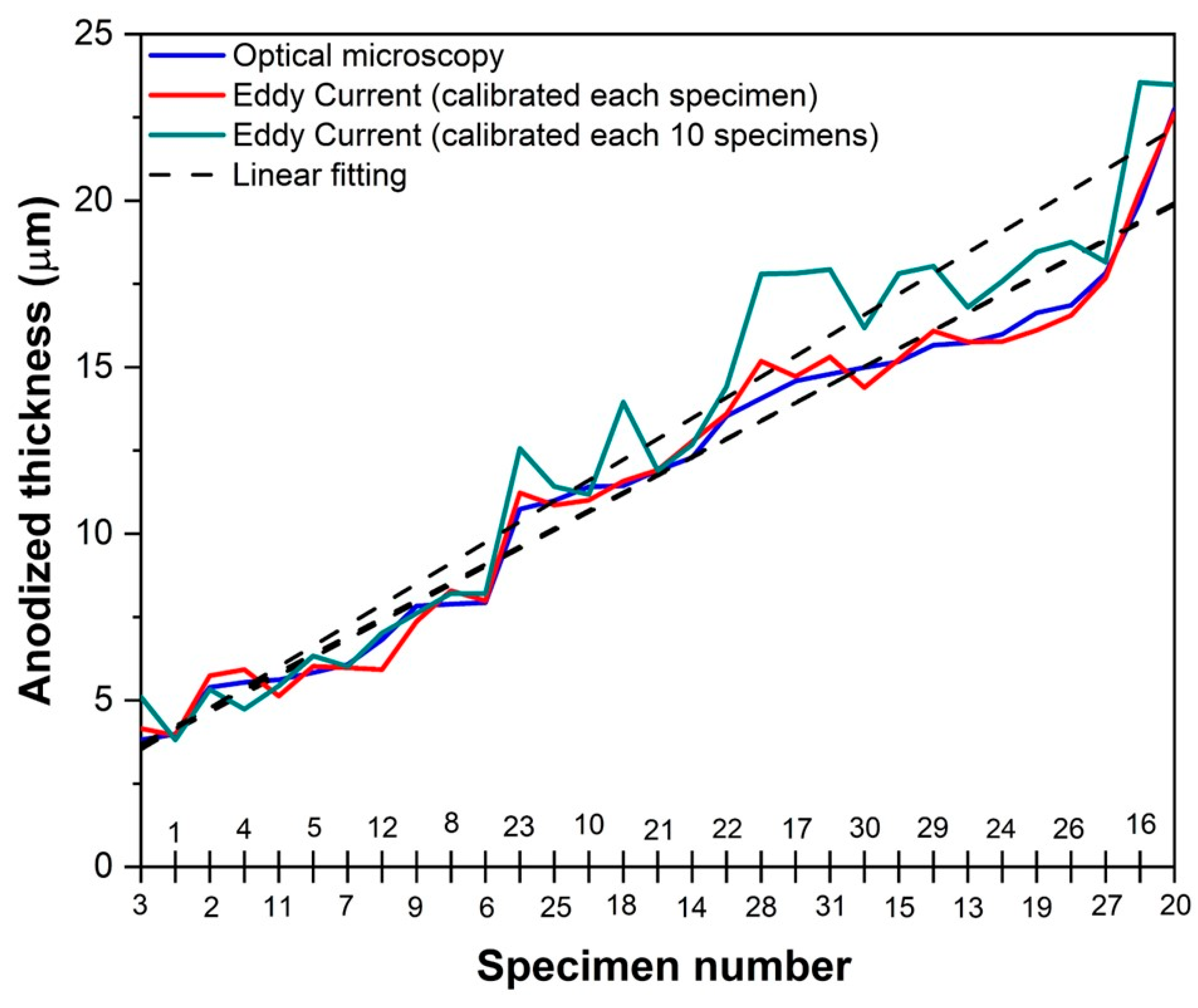
Additionally, Figure 6 presents the anodized layer thickness measurements arranged from the lowest to the highest values. The measurements obtained using the calibration methodology performed before each individual reading (with an average error of 3.4%) show close agreement with the reference values obtained through optical microscopy, which reinforces the accuracy of this approach. In contrast, when the calibration was performed every 10 specimens, the results were less consistent, particularly as the thickness of the anodized layer increased. In cases involving thicker anodized coatings, the discrepancy between the Eddy current results and those from optical microscopy became more pronounced, indicating that this spaced calibration methodology is not suitable for obtaining accurate measurements of thicker anodized layers. Figure 6 shows the linear fitting lines for the different measurements, where it can clearly be seen that the thickness measurements obtained using an optical microscope and Eddy current, calibrated before each measurement, overlap, indicating that there is a good correlation between the measurements. However, when calibration occurs every ten specimens, the linear fit deviates from the optical microscopy measurement, indicating that errors may occur in the measurement with this calibration interval of every ten specimens.
This analysis reveals that Eddy current testing, when the equipment is properly calibrated before each measurement, can be an effective and rapid method for measuring the thickness of the anodized layer. However, it is evident that the calibration frequency plays a fundamental role in the accuracy of the measurements. Frequent calibration ensures more reliable results, while less frequent calibration can lead to greater margins of error.

3.3. Comparison of Measurement Methods

3.3.1. Bland–Altman Method for Measurement with Calibration

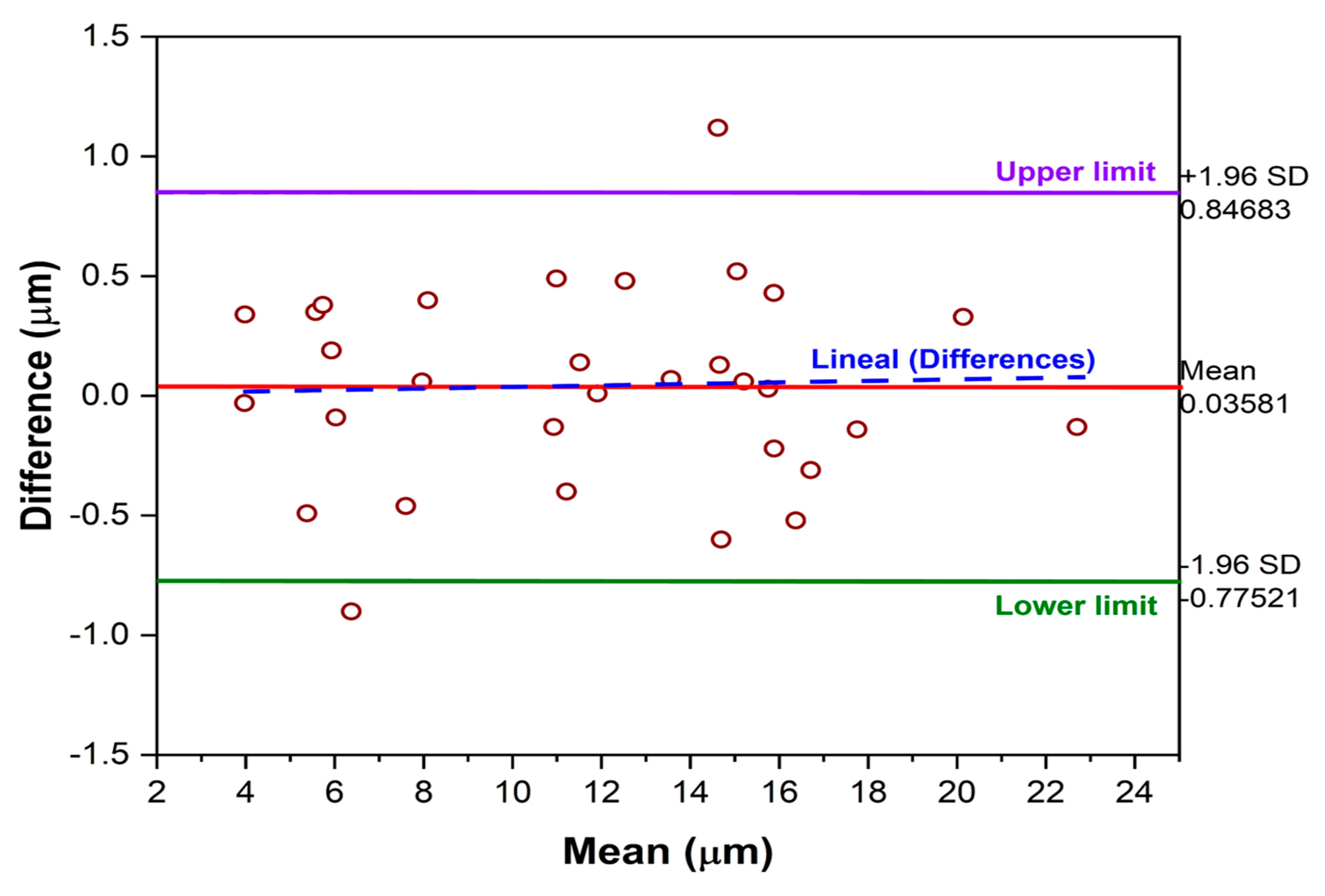
Figure 7 presents the Bland–Altman plot corresponding to the comparison between the established method of optical microscopy and the Eddy current method, in which the equipment was calibrated before each measurement. For the construction of the plot, a mean bias d ¯ of 0.033 μm was determined, while the limits of agreement were calculated as 0.844 μm for the upper limit and −0.777 μm for the lower limit.
The positive bias of 0.033 μm indicates that, on average, the Eddy current measurement method, when calibrated before each measurement, tends to slightly overestimate the thickness compared to the optical microscopy method. In other words, the measurements obtained using Eddy current are, on average, 0.033 μm higher than those obtained with optical microscopy. Additionally, the mean difference line, or bias line, is located very close to the line of perfect agreement at a value of zero [21,38,39]. This result suggests that there is no significant systematic difference between the two methods. Consequently, it can be stated that the measurements obtained using both methods are comparable and reliable within the context of this study.
On the other hand, the limits of agreement, set at 0.844 μm (upper limit) and −0.777 μm (lower limit), indicate that approximately 95% of the differences between measurements from both methods fall within this range [40,41]. These values suggest that, in most cases, the differences between the two methods do not exceed ±1 μm, which supports a good level of agreement. The fact that these limits are relatively narrow further reinforces the evidence that the new method demonstrates acceptable accuracy in comparison with the reference method.
In the Bland–Altman plot, two points are observed outside the limits of agreement, which is consistent with the fact that 95% of the differences are expected to lie within those limits. This implies that the presence of approximately 5% of the points falling outside the limits is statistically expected and does not necessarily indicate a failure of the method [42]. These points represent isolated discrepancies between the measurements of both methods, but since the recorded differences are in the order of 1 μm, they are considered to have no significant impact within the context of this research.
From a practical perspective, these outlier values do not substantially affect the overall agreement between the methods, and therefore, there is no justification to conclude that the new method is not interchangeable with the reference method.
Additionally, a trend line was incorporated into the graph, which displays a slightly positive slope. This suggests that as the average thickness of the anodized layer increases, the difference between the two methods also tends to increase slightly [43,44]. However, this trend is minimal and does not significantly impact the overall agreement between the evaluated methods.
Finally, based on the results obtained from the Bland–Altman plot, it can be stated that the Eddy current measurement method, when calibrated prior to the measurement of each sample, shows a high level of agreement with the established optical microscopy method. This is evidenced by the calculated bias d ¯ = 0.033   μ m , which is a value very close to zero, indicating that, on average, the measurements obtained with the new method are equivalent to those of the traditional method [45,46].

3.3.2. Bland–Altman Method for Measurement with Calibration Every 10 Specimens

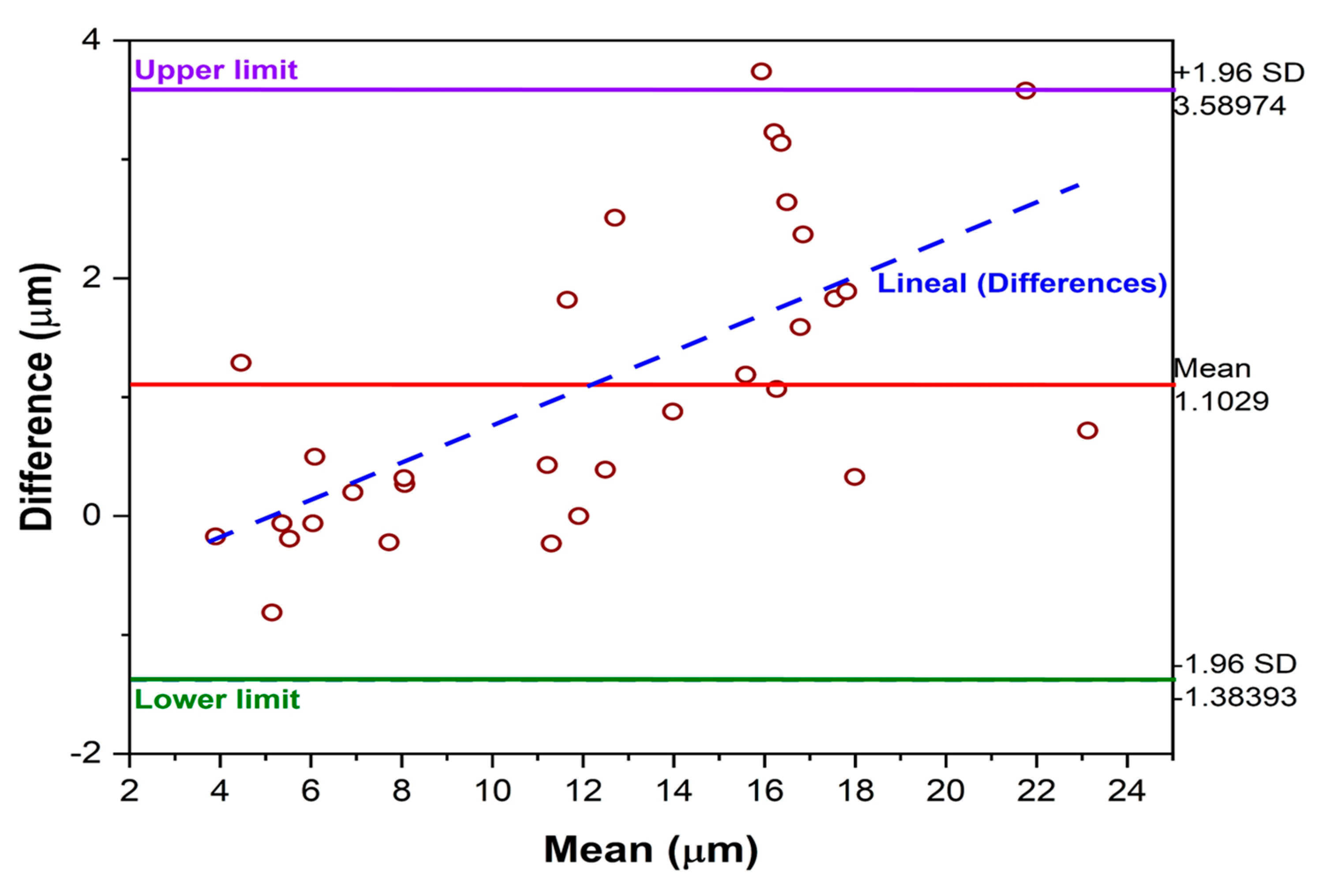
Figure 8 presents the Bland–Altman plot corresponding to the comparison between the reference method of optical microscopy and the Eddy current method, with equipment calibration performed every 10 measurements. For the construction of the plot, a bias d ¯ of 1.10 μm was determined, while the limits of agreement were calculated at 3.59 μm for the upper limit and −1.39 μm for the lower limit.
The bias value for this method comparison indicates that the new method overestimates the measurements; that is, on average, the results obtained using Eddy current are 1.1 μm higher than those obtained with optical microscopy. In the case of Eddy currents, the overestimations of values when performing calibration every ten samples may be due to different factors, such as skin effect and edge effect. In the case of skin effect, Eddy currents are concentrated near the surface of the material, which limits the depth at which defects or changes in properties can be detected. The presence of edges (edge effect) can cause a higher concentration of currents in those areas, which generates false signals or distortions in the measurement [47,48,49]. This method presents a considerably greater bias, indicating the presence of a systematic difference between the two methods. This is easily identifiable in the plot, as most of the differences are distributed above the line of perfect agreement (value of zero). This demonstrates a tendency of the new thickness measurement method using Eddy current with calibration every 10 measurements to overestimate the original value by an average of 1.1 μm.
This trend can be clearly observed in Figure 8, where it is evident that as the thickness of the anodized layer increases, so does the difference between the measurements obtained with the reference method and those obtained using the new method with calibration every 10 specimens. This behavior indicates that the agreement between both methods decreases as the measured thickness increases, suggesting that the calibration frequency negatively affects the accuracy of the new method in higher thickness ranges [50,51,52].
On the other hand, the values obtained for the limits of agreement—3.59 μm for the upper limit and −1.39 μm for the lower limit—indicate that 95% of the differences between both measurement methods fall within this range. This interval represents a considerably wider range compared to the one obtained when the equipment is calibrated before each specimen, which demonstrates greater dispersion in the results of the new method. The width of these limits suggests the presence of significant variability in the measurements taken with the Eddy current method calibrated every 10 specimens, resulting in lower precision compared to the reference method.
In Figure 8, one point is observed outside the limits of agreement, which represents an outlier. However, this result corresponds to less than 5% of the data, which is consistent with what is statistically expected in a Bland–Altman analysis, where approximately 95% of the differences are predicted to fall within the agreement interval. Moreover, this point follows the trend observed in the remainder of the data. Therefore, this outlier does not represent a significant discrepancy nor suggest errors in the measurement process but can be attributed to the inherent variability of the method and the systematic trend already identified [53,54,55,56]. The Bland–Altman procedure assumes that both methods being compared have measurement errors, i.e., neither is the reference method; therefore, the mean of the two measurements is the best estimate available for plotting the graph [4,57,58,59]. However, even if there is a reference method, there may always be doubt as to whether the measurements are performed without any error; therefore, the 95% concordance limits are also a valid measure of the possible difference between the new method and the reference method [60].
Furthermore, in Figure 8, it is possible to identify a trend line with a steep positive slope, indicating that as the anodized layer thickness increases, the difference between the measurement methods also increases. This trend suggests that the method involving the calibration of the equipment every 10 specimens does not maintain good agreement with the reference method, particularly in measurements of greater thickness. In other words, the accuracy of the new method decreases as the anodized layer thickness increases, highlighting a limitation related to the calibration frequency.
Finally, based on the results obtained from comparing the established optical microscopy method with the Eddy current method, where the equipment was calibrated every 10 measurements, it can be concluded that the new method is applicable when the measured thicknesses are small. As mentioned in Section 3.2.2, when the average thickness is approximately between 5 and 10 μm, most of the differences are close to the perfect agreement line (zero value). However, starting from a thickness of 10 μm, the differences in the results steadily increase. For this reason, along with the observed bias, we can confirm that this method is not equivalent for all measurements, and therefore, not equivalent to the reference method.

4. Conclusions

  • A comparative analysis of the traditional optical microscopy measurement method and the Eddy current method, utilizing various calibration frequencies to ascertain the anodized layer thickness in a 6063 aluminum alloy, facilitated a thorough assessment of the concordance, precision and applicability of the novel method under controlled conditions.
  • Since optical microscopy can only measure a certain portion of the specimen that has undergone metallographic preparation, it cannot offer a comprehensive assessment of the thickness of the anodized layer.
  • The results obtained using the Eddy current method demonstrate that calibrating the device before each measurement is the most accurate option, since it presents an error percentage of 3.4%.
  • Calibrating the device every 10 samples yields an error rate of 9.9%, indicating that the first methodology is approximately three times more accurate.
  • The use of the Eddy current device enables the determination of anodized layer thickness at multiple locations along the specimen, which facilitates a more effective detection of layer uniformity than the optical microscopy method.
  • The results show that calibrating the device prior to each measurement is the most accurate option, since the Eddy current method yields an error percentage of 3.4%.
  • The method of calibrating Eddy currents every ten samples presented a greater error with respect to the reference method and overestimated the thickness by 1.10 μm with respect to the reference value obtained via optical microscopy.
  • The Bland–Altman analysis for the Eddy current method calibrated every 10 specimens revealed an increasing trend in the discrepancy between methods as the thickness of the anodized layer increased.
  • Calibration is a determining factor in the accuracy of the alternative method; the results are acceptable for lower thicknesses, since with thicknesses greater than 15 μm, the deviations in the measurements become more noticeable.

Research Limitations

  • For this research, only anodized 6063 aluminum alloy materials were used, where the current density, time and concentration of the solution were varied, and the effect of each parameter on the coating thickness was not evaluated.
  • This work only presents data from optical microscopy and Eddy current thickness measurements in a 6063 aluminum alloy. The results may not be applicable to other aluminum alloys due to the composition of the alloys, the heat treatments applied, the anodization parameters, such as time, solution concentration and applied current density, and the parameters involved in the measurements.
  • The thickness measurement range of between 3 and 25 μm is derived from the anodization conditions used on the samples. These anodization conditions are presented in Table 2 of this document.
  • The number of samples used in this study is limited, as they are samples used in the design of experiments focused on evaluating the effects of process variables on the characteristics of anodization, which is not the objective of this research study.

Author Contributions

Conceptualization, J.C.-M. and F.A.-C.; methodology, D.N.-M., D.V.C., M.L.-B., E.M.-B., C.T.M.-R. and M.A.B.-Z.; data curation, E.M.-B., J.O.-C., D.V.C., D.N.-M., J.C.-M., C.G.-T. and C.T.M.-R.; formal analysis, F.A.-C., M.L.-B., C.G.-T., J.C.-M., M.A.B.-Z., J.O.-C. and C.T.M.-R.; validation, J.C.-M., F.A.-C. and C.G.-T.; writing—original draft preparation, J.C.-M., D.V.C. and F.A.-C.; writing—review and editing, J.C.-M. and F.A.-C. All authors have read and agreed to the published version of the manuscript.

Funding

This research was funded by “Programa de Apoyo a la Ciencia, Tecnología e Innovación 2023 y 2024 de la Universidad Autónoma de Nuevo León”, grant number 133-IDT-2023 and 15-IDT-2024.

Institutional Review Board Statement

Not applicable.

Informed Consent Statement

Not applicable.

Data Availability Statement

The raw data supporting the conclusions of this article will be made available by the authors on request.

Acknowledgments

The authors acknowledge the academic body UANL—CA-316 “Deterioration and integrity of composite materials” and the student Ing. Lino Jesús Juárez Alejandro.

Conflicts of Interest

The authors declare no conflicts of interest.

References

  1. Muñoz, J.A.; Komissarov, A.; Avalos, M.; Bolmaro, R.E. Heat Treatment effect on an AA6063 alloy. Mater. Lett. 2020, 277, 128338. [Google Scholar] [CrossRef]
  2. Muñoz, J.A.; Khelfa, T.; Duarte, G.A.; Avalos, M.; Bolmaro, R.; Cabrera, J.M. Plastic Behavior and Microstructure Heterogeneity of an AA6063-T6 Aluminum Alloy Processed by Symmetric and Asymmetric Rolling. Metals 2022, 12, 1551. [Google Scholar] [CrossRef]
  3. Bensalah, W.; Elleuch, K.; Feki, M.; Gigandet, M.P.; Ayedi, H.F. Optimization of mechanical and chemical properties of sulphuric anodized aluminium using statistical experimental methods. Mat. Chem. Phys. 2008, 108, 296–305. [Google Scholar] [CrossRef]
  4. Martínez-Ramos, C.; Olguin-Coca, J.; Lopez-Leon, L.D.; Gaona-Tiburcio, C.; Lara-Banda, M.; Maldonado-Bandala, E.; Castañeda-Robles, I.; Jaquez-Muñoz, J.M.; Cabral-Miramontes, J.; Nieves-Mendoza, D.; et al. Electrochemical Noise Analysis Using Experimental Chaos Theory, Power Spectral Density and Hilbert–Huang Transform in Anodized Aluminum Alloys in Tartaric–Phosphoric–Sulfuric Acid Solutions. Metals 2023, 13, 1850. [Google Scholar] [CrossRef]
  5. Vergara-Guillén, L.E.; Nerey-Carvajal, L.M.; Guedez Torcates, V.M. Oxide film thickness and microhardness prediction model of Al3003-B14 and Al6063-T6 anodized aluminum using multifactorial analysis. Ingeniare Rev. Chil. De Ing. 2011, 19, 186–195. [Google Scholar] [CrossRef]
  6. Thompson, G.E. Porous anodic alumina: Fabrication, characterization and applications. Thin Solid Films 1997, 297, 192–201. [Google Scholar] [CrossRef]
  7. ASTM B487-85; Standard Test Method for Measurement of Metal and Oxide Coating Thickness by Microscopical Examination of Cross Section. ASTM International: West Conshohocken, PA, USA, 2020.
  8. Chen, L.; Zhou, Y.; Zhou, R.; Hong, M. Microsphere-Toward future of optical microscopes. Iscience 2020, 23, 101211. [Google Scholar] [CrossRef]
  9. Giurlani, W.; Berretti, E.; Innocenti, M.; Lavacchi, A. Measuring the Thickness of Metal Coatings: A Review of the Methods. Coatings 2020, 10, 1211. [Google Scholar] [CrossRef]
  10. Machado, M.A. Eddy Currents Probe Design for NDT Applications: A Review. Sensors 2024, 24, 5819. [Google Scholar] [CrossRef]
  11. Sitko, R. Quantitative X-ray fluorescence analysis of samples of less than “infinite thickness”: Difficulties and possibilities. Spectrochim. Acta Part B At. Spectrosc. 2009, 64, 1161–1172. [Google Scholar] [CrossRef]
  12. Lopes, F.; Cardozo Amorin, L.H.; da Silva Martins, L.; Urbano, A.; Roberto Appoloni, C.; Cesareo, R. Thickness measurement of V2O5 nanometric thin films using a portable XRF. J. Spectrosc. 2016, 2016, 9509043. [Google Scholar] [CrossRef]
  13. Criss, J.W.; Birks, L.S. Calculation methods for fluorescent X-ray spectrometry: Empirical coefficients vs. fundamental parameters. Anal. Chem. 1968, 40, 1080–1086. [Google Scholar] [CrossRef]
  14. Giurlani, W.; Berretti, E.; Lavacchi, A.; Innocenti, M. Thickness determination of metal multilayers by ED-XRF multivariate analysis using Monte Carlo simulated standards. Anal. Chim. Acta 2020, 1130, 72–79. [Google Scholar] [CrossRef]
  15. Giurlani, W.; Berretti, E.; Innocenti, M.; Lavacchi, A. Coating Thickness determination using X-ray fluorescence spectroscopy: Monte Carlo simulations as an alternative to the use of standards. Coatings 2019, 9, 79. [Google Scholar] [CrossRef]
  16. Pessanha, S.; Manso, M.; Antunes, V.; Carvalho, M.L.; Sampaio, J.M. Monte Carlo simulation of portable X-ray fluorescence setup: Non-invasive determination of gold leaf thickness in indo-Portuguese panel paintings. Spectrochim. Acta Part B At. Spectrosc. 2019, 156, 1–6. [Google Scholar] [CrossRef]
  17. Malarde, D.; Powell, M.J.; Quesada-Cabrera, R.; Wilson, R.L.; Carmalt, C.J.; Sankar, G.; Parkin, I.P.; Palgrave, R.G. Optimized atmospheric-pressure chemical vapor deposition thermochromic VO2 thin films for intelligent window applications. ACS Omega 2017, 2, 1040–1046. [Google Scholar] [CrossRef]
  18. Krumrey, M.; Gleber, G.; Scholze, F.; Wernecke, J. Synchrotron radiation-based X-ray reflection and scattering techniques for dimensional nanometrology. Meas. Sci. Technol. 2011, 22, 094032. [Google Scholar] [CrossRef]
  19. Serafi’nczuk, J.; Pietrucha, J.; Schroeder, G.; Gotszalk, T.P. Thin film thickness determination using X-ray reflectivity and Savitzky-Golay algorithm. Opt. Appl. 2011, 41, 315–322. [Google Scholar]
  20. Sokolov, S.A.; Milovanov, R.A.; Sidorov, L.N. Determination of the thickness of thin films based on scanning electron microscopy and energy dispersive X-ray analysis. J. Surf. Investig. X-ray Synchrotron Neutron Tech. 2019, 13, 836–847. [Google Scholar] [CrossRef]
  21. Goldstein, J.I.; Newbury, D.E.; Michael, J.R.; Ritchie, N.W.M.; Scott, J.H.J.; Joy, D.C. Scanning Electron Microscopy and X-Ray Microanalysis; Springer Publishing: New York, NY, USA, 2018; ISBN 978-1-4939-6674-5. [Google Scholar]
  22. Jablonski, A. Evaluation of procedures for overlayer thickness determination from XPS intensities. Surf. Sci. 2019, 688, 14–24. [Google Scholar] [CrossRef]
  23. Walton, J.; Alexander, M.R.; Fairley, N.; Roach, P.; Shard, A.G. Film thickness measurement and contamination layer correction for quantitative XPS. Surf. Interface Anal. 2016, 48, 164–172. [Google Scholar] [CrossRef]
  24. Cumpson, P.J. The thickogram: A method for easy film thickness measurement in XPS. Surf. Interface Anal. 2000, 29, 403–406. [Google Scholar] [CrossRef]
  25. Nave, F.; Nave, J. Técnicas estadísticas utilizadas en la comparación de métodos cuantitativos de medición. Cienc. Tecnol. Sal. 2023, 10, 53–75. [Google Scholar] [CrossRef]
  26. Myung, J.I.; Pitt, M.A. Model comparison methods. Methods Enzymol. 2004, 383, 351–366. [Google Scholar] [CrossRef]
  27. Deng, W.; Wang, J.; Zhang, R. Measures of concordance and testing of independence in multivariant structure. J. Multivar. Anal. 2022, 191, 105035. [Google Scholar] [CrossRef]
  28. Tommervik, L.; Shreiber, D.; Pope, D. Comparing Thickness Measurement Methods Using Bland–Altman Analysis. DEVCOM ARL 2021, 9326. Available online: https://apps.dtic.mil/sti/trecms/pdf/AD1149580.pdf (accessed on 12 April 2025).
  29. Cabral Miramontes, J.C.; Gaona Tiburcio, C.; García Mata, E.; Esneider Alcála, M.Á.; Maldonado-Bandala, E.; Lara-Banda, M.; Nieves-Mendoza, D.; Olguín-Coca, J.; Zambrano-Robledo, P.; López-León, L.D.; et al. Corrosion Resistance of Aluminum Alloy AA2024 with Hard Anodizing in Sulfuric Acid-Free Solution. Materials 2022, 15, 6401. [Google Scholar] [CrossRef]
  30. Cabral-Miramontes, J.; Almeraya-Calderón, F.; López, F.E.; Lara Banda, M.; Olguín-Coca, J.; López-León, L.D.; Castañeda-Robles, I.; Alcalá, M.Á.E.; Zambrano-Robledo, P.; Gaona-Tiburcio, C. Citric Acid as an Alternative to Sulfuric Acid for the Hard-Anodizing of AA6061. Metals 2021, 11, 1838. [Google Scholar] [CrossRef]
  31. Jáquez-Muñoz, J.M.; Gaona-Tiburcio, C.; Chacón-Nava, J.; Cabral-Miramontes, J.; Nieves-Mendoza, D.; Maldonado-Bandala, E.M.; Delgado, A.D.; Flores-De Los Rios, J.P.; Bocchetta, P.; Almeraya-Calderón, F. Electrochemical Corrosion of Titanium and Titanium Alloys Anodized in H2SO4 and H3PO4 Solutions. Coatings 2022, 12, 325. [Google Scholar] [CrossRef]
  32. ASTM E3-95; Standard Practice for Preparation of Metallographic Specimens. ASTM International: West Conshohocken, PA, USA, 1995.
  33. Sardellitti, A.; Milano, F.; Laracca, M.; Ventre, S.; Ferrigno, L.; Tamburrino, A. An Eddy-Current Testing Method for Measuring the Thickness of Metallic Plates. IEEE Trans. Instrum. Meas. 2023, 72, 1–10. [Google Scholar] [CrossRef]
  34. Liu, P.; Singh, V.P.; Rajaputra, S. Barrier layer non-uniformity effects in anodized aluminum oxide nanopores on ITO substrates. Nanotechnology 2010, 21, 115303. Available online: https://iopscience.iop.org/article/10.1088/0957-4484/21/11/115303 (accessed on 12 February 2025). [CrossRef]
  35. Pu, Y.; Hu, J.; Yao, T.; Li, L.; Zhao, J.; Guo, Y. Influence of anodization parameters on film thickness and volume expansion of thick- and large-sized anodic aluminum oxide film. J. Mater. Sci. Mater. Electron. 2021, 32, 13708–13718. [Google Scholar] [CrossRef]
  36. Villegas-Tovar, J.; Gaona-Tiburcio, C.; Lara-Banda, M.; Maldonado-Bandala, E.; Baltazar-Zamora, M.A.; Cabral-Miramontes, J.; Nieves-Mendoza, D.; Olguin-Coca, J.; Estupiñan-Lopez, F.; Almeraya-Calderón, F. Electrochemical Corrosion Behavior of Passivated Precipitation Hardening Stainless Steels for Aerospace Applications. Metals 2023, 13, 835. [Google Scholar] [CrossRef]
  37. Rodger, J.; Bartlett, S.; Atrens, A. Corrosion of the galvanizing of galvanized-steel electricity transmission towers. Mater. Corros. 2017, 68, 902–910. [Google Scholar] [CrossRef]
  38. Bland, J.M.; Altman, D.G. Statical methods for assessing agreement between two methods of clinical measurements. Lancet 1986, 327, 307–310. [Google Scholar] [CrossRef]
  39. Yellareddygari, S.K.R.; Gudmestad, N.C. Bland-Altman comparison of two methods for assessing severity of Verticillium wilt of potato. Crop Prot. 2017, 101, 68–75. [Google Scholar] [CrossRef]
  40. Tiptona, E.; Shusterb, J. A framework for the meta-analysis of Bland–Altman studies based on a limits of agreement approach. Stat. Med. 2017, 36, 3621–3635. [Google Scholar] [CrossRef]
  41. Goedhart, J.; Rishniw, M. BA-plotteR—A web tool for generating Bland-Altman plots and constructing limits of agreement. Res. Vet. Sci. 2021, 137, 281–286. [Google Scholar] [CrossRef]
  42. Moore, A.R. A review of Bland–Altman difference plot analysis in the veterinary clinical pathology laboratory. Vet. Clin. Pathol. 2024, 53, 75–85. [Google Scholar] [CrossRef]
  43. Mansournia, M.; Waters, R.; Nazemipour, M.; Bland, M.; Altman, D. Bland-Altman methods for comparing methods of measurement and response to criticisms. Glob. Epidemiol. 2021, 3, 100045. [Google Scholar] [CrossRef]
  44. Haghayegh, S.; Kang, H.; Khoshnevis, S.; Smolensky, M.; Diller, K. A comprehensive guideline for Bland–Altman and intra class correlation calculations to properly compare two methods of measurement and interpret findings. Physiol. Meas. 2020, 41, 055012. [Google Scholar] [CrossRef]
  45. Doğan, N.O. Bland-Altman analysis: A paradigm to understand correlation and agreement. TJEM 2018, 18, 139–141. [Google Scholar] [CrossRef] [PubMed]
  46. Giavarina, D. Understanding Bland Altman analysis. Biochem. Med. 2015, 25, 141–151. [Google Scholar] [CrossRef]
  47. Almeida, G.; Gonzalez, J.; Rosado, L.; Vilaça, P.; Santos, T.G. Advances in NDT and materials characterization by eddy currents. Procedia CIRP 2013, 7, 359–364. [Google Scholar] [CrossRef]
  48. Xie, Y.; Li, J.; Tao, Y.; Wang, S.; Yin, W.; Xu, L. Edge Effect Analysis and Edge Defect Detection of Titanium Alloy Based on Eddy Current Testing. Appl. Sci. 2020, 10, 8796. [Google Scholar] [CrossRef]
  49. Wang, Y.; Bai, Q.; Du, W.; Zhang, B. Edge Effect on Eddy Current Detection for Subsurface Defects in Titanium Alloys. In Proceedings of the 8th International Conference on Computational Methods (ICCM2017), Guilin, China, 25–29 July 2017. [Google Scholar]
  50. Gerke, O. Reporting Standards for a Bland–Altman Agreement Analysis: A Review of Methodological Reviews. Diagnostics 2020, 10, 334. [Google Scholar] [CrossRef] [PubMed]
  51. Flegal, K.M.; Graubard, B.; Ioannidis, J.P.A. Use and reporting of Bland–Altman analyses in studies of self-reported versus measured weight and height. IJO 2020, 44, 1311–1318. [Google Scholar] [CrossRef]
  52. ISO 21968:2019; Non-magnetic metallic coatings on metallic and non-metallic basis materials—Measurement of coating thickness—Phase-sensitive eddy-current method. International Organization for Standardization: Geneva, Switzerland, 2019. Available online: https://www.iso.org/standard/73285.html (accessed on 4 March 2025).
  53. Francq, B.G.; Govaerts, B. How to regress and predict in a Bland–Altman plot? Review and contribution based on tolerance intervals and correlated-errors-in-variables models. Stat. Med. 2016, 35, 2328–2358. [Google Scholar] [CrossRef] [PubMed]
  54. Sato, H.; Miyata, K.; Yoshikawa, K.; Mizukami, M. A comparison between the shoulder shifting test and seated reaching test by bland–altman plot: A pilot study. J. Spinal Cord Med. 2022, 47, 522–529. [Google Scholar] [CrossRef]
  55. Cabral, J.; Pedraza, G.K.; Gaona, C.; Zambrano, P.; Poblano, C.A.; Almeraya, F. Coatings characterization of Ni-based alloy applied by HVOF. Aircr. Eng. Aerosp. Tec. 2018, 90, 336–343. [Google Scholar] [CrossRef]
  56. Gaona-Tiburcio, C.; Montoya, R.M.; Cabral, M.J.A.; Estupiñan, L.F.; Zambrano, R.P.; Orozco, C.R.; Chacon-Nava, J.G.; Baltazar, Z.M.A.; Almeraya-Calderon, F. Corrosion Resistance of Multilayer Coatings Deposited by PVD on Inconel 718 Using Electrochemical Impedance Spectroscopy Technique. Coatings 2020, 10, 521. [Google Scholar] [CrossRef]
  57. Bland, J.M.; Altman, D.G. Comparing methods of measurement: Why plotting difference against standard method is misleading. Lancet 1995, 346, 1085–1087. [Google Scholar] [CrossRef]
  58. Carrasco, J.L.; Jover, L. Métodos estadísticos para evaluar la concordancia. Med. Clin. 2004, 122 (Suppl. 1), 28–34. Available online: https://www.elsevier.es/es-revista-medicina-clinica-2-articulo-metodos-estadisticos-evaluar-concordancia-13057543 (accessed on 12 February 2025). [CrossRef]
  59. Samaniego-Gámez, P.; Almeraya-Calderón, F.; Martin, U.; Ress, J.; Gaona-Tiburcio, C.; Silva-Vidaurri, L.; Cabral-Miramontes, J.; Bastidas, J.M.; Chacón-Nava, J.G.; Bastidas, D.M. Efecto del tratamiento de sellado en el comportamiento frente a corrosión de la aleación anodizada de aluminio-litio AA2099. Rev. Met. 2020, 56, e180. [Google Scholar] [CrossRef]
  60. Bland, J.M.; Altman, D.G. Comparing two methods of clinical measurement: A personal history. Int. J. Epidem. 1995, 24 (Suppl. 1), S7–S14. [Google Scholar] [CrossRef] [PubMed]
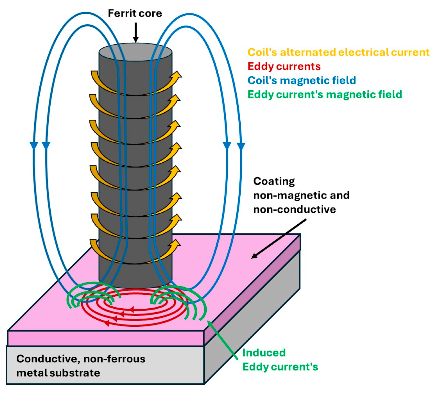
Figure 1. Eddy currents produce a secondary magnetic field that opposes the coil’s initial magnetic field.
Applsci 15 09025 g001
Figure 2. Thickness measured via optical microscopy. (a) Specimen 3 at 500×, (b) Specimen 3 at 1000×, (c) Specimen 17 at 500×, (d) Specimen 19 at 500× and (e) Specimen 20 at 500×.
Applsci 15 09025 g002
Figure 3. Comparison of anodized layer thicknesses (calibrated before each specimen).
Applsci 15 09025 g003
Figure 4. Comparison of anodized layer thicknesses (calibrated every 10 specimens).
Applsci 15 09025 g004
Figure 6. Anodized coating thickness comparison in ascending order.
Applsci 15 09025 g006
Figure 7. Bland–Altman plot of optical microscopy vs. Eddy current (calibration for each specimen).
Applsci 15 09025 g007
Figure 8. Bland–Altman plot of optical microscopy vs. Eddy current (calibration every 10 specimens).
Applsci 15 09025 g008
Table 1. Chemical composition obtained via X-ray fluorescence of aluminum 6063.
ElementsAlSiFeCuMnMgCrTiZn
AA 6063Bal0.550.060.0040.0060.830.0020.0020.007
NominalBal0.20–0.600.0–0.350.0–0.100.0–0.100.45–0.900.0–0.100.0–0.100.0–0.10
Table 2. Different conditions of the anodized samples.
Specimen NumberTime (min)Current Density of Anodized Samples (A/dm2)Concentration of H2SO4 (g/L)Specimen NumberTime (min)Current Density of Anodized Samples (A/dm2)Concentration of H2SO4 (g/L)
1101.2718017152.5180
2101.7918018152.5350
3101.2735019153.5350
4101.7935020153.5180
5151.2718021261.5180
6151.7918022301.5180
7151.273502313.53.0265
8151.793502421.73.0265
9201.273502517.52.15265
10201.793502617.53.84265
11260.761802717.53.842.65
12300.761802817.53.0122
13202.51802917.53.0407
14202.53503017.53.0265
15203.53503117.53.02.65
16203.5180
Table 3. Results of the thicknesses obtained with both methods.
Specimen NumberOptical Microscopy
(μm)
Eddy Current Calibrated for Each Specimen
(μm)
Eddy Current Calibrated Every 10 Specimens
(μm)
13.983.953.81
25.395.745.33
33.814.155.1
45.545.924.73
55.836.026.33
67.937.998.2
76.075.986.01
87.898.298.21
97.837.377.61
1011.4111.0111.18
115.625.135.43
126.825.927.02
1315.7315.7616.8
1412.2912.7712.68
1515.1715.2317.81
1619.9720.323.55
1714.5914.7217.82
1811.4411.5813.95
1916.6316.1118.46
2022.7622.6323.48
2111.911.9111.9
2213.5313.614.41
2310.7411.2312.56
2415.9915.7717.58
2510.9910.8611.42
2616.8616.5518.75
2717.8217.6818.15
2814.0615.1817.8
2915.6616.0918.03
3014.9914.3916.18
3114.7915.3117.93
Disclaimer/Publisher’s Note: The statements, opinions and data contained in all publications are solely those of the individual author(s) and contributor(s) and not of MDPI and/or the editor(s). MDPI and/or the editor(s) disclaim responsibility for any injury to people or property resulting from any ideas, methods, instructions or products referred to in the content.