Article

Research on the Application of Laser Ablation in the Rapid Detection of Ablation Resistance on the Surface of AgNi Contact Materials

State Key Laboratory of Intelligent Power Distribution Equipment and System, Hebei University of Technology, Tianjin 300401, China
*
Author to whom correspondence should be addressed.
These authors contributed equally to this work.
Appl. Sci. 2025, 15(16), 8961; https://doi.org/10.3390/app15168961
Submission received: 28 July 2025 / Revised: 10 August 2025 / Accepted: 12 August 2025 / Published: 14 August 2025
(This article belongs to the Section Electrical, Electronics and Communications Engineering)

Abstract

The ablation resistance of electrical contact materials is a key factor in ensuring the long-term stable operation of electrical equipment. However, conventional electrical contact tests often suffer from long testing cycles, high resource consumption, and poor repeatability, which severely limits the efficient screening and engineering application of new materials. In this study, the thermal erosion behavior of AgNi-series silver-based contact materials under various laser energy inputs was systematically investigated using laser ablation technology. An integrated laser testing platform was employed to extract multiple parameters, including longitudinal ablation depth, linear ablation rate, depth-to-diameter ratio, and ablation area growth rate, enabling quantitative analysis of thermal response characteristics and performance comparison among materials. Furthermore, fractal dimension analysis was introduced to characterize the evolution of surface morphological complexity after ablation, and Pearson correlation analysis was performed to compare the results with those from conventional electrical contact tests. The results showed high consistency in ablation resistance ranking and surface response trends between the two methods, with correlation coefficients for all three materials exceeding 0.78, and AgNi10 exhibiting the best ablation resistance. This study demonstrates that laser ablation technology can significantly shorten testing cycles and improve repeatability while ensuring result reliability, providing an efficient and feasible approach for high-throughput screening and industrial application of electrical contact materials.

1. Introduction

In modern electrical engineering and equipment design, choosing the right contact materials has become an important part of ensuring systems work smoothly and last longer [1]. As electronics become smaller, lighter, and able to handle more power [2], the current running through contact materials has gone up considerably [3,4]. During contact closing, the heat from electrical resistance can cause static fusion welding, and during breaking, high-temperature arcs can lead to material erosion. Both of these issues demand contact materials that can conduct heat well and resist damage from high temperatures. These qualities are directly linked to how stable and durable the electrical components are [5,6,7].
Silver-based contact materials, like AgNi and AgSnO2, are common choices for key parts, such as low-voltage circuit breakers and high-voltage DC relays, because they have low resistance and good ability to transfer heat, and they resist oxidation at high temperatures [8,9,10]. Traditionally, evaluating these materials’ stability and resistance to erosion involves arc switching tests, which can be slow, use a lot of material, and are not always efficient for improving performance [11,12,13]. Recently, laser technology has become popular for studying how these materials behave under thermal shock and ablation, thanks to its high energy density and precise control. Laser ablation methods have been used in aerospace [14], metallurgy [15], and composite materials research [16,17], and are now being applied to electrical contact material testing because they are easy to use, repeatable, and cost-effective. Researchers like Liu Songtao [18,19] have used laser simulation arc tests to analyze how doping elements affect contact materials, discovering that adding elements like lanthanum greatly improves resistance to ablation, and adding copper helps with wettability and overall performance. Studies by Wang J. [20] and others looked into how adding CuO influences the formation of protective layers in Ag-SnO2 materials, finding that it improves the microstructure and durability. Also, Dong Bowen [21] used laser simulation ablation to understand how Cu-W alloys behave at high temperatures, helping to guide the design of better electrical contact materials.
Beyond laboratory applications, the advancement of modern industrial systems has created an increasing demand for intelligent monitoring and predictive maintenance strategies that can incorporate rapid material assessment techniques, particularly in harsh operating environments. Recent studies have demonstrated the successful integration of embedded sensors and electronic circuits for monitoring machinery operating conditions in challenging industrial settings, such as wastewater treatment facilities [22,23,24]. These investigations have proposed generalizable intelligent detection algorithms and artificial intelligence approaches for diagnosing material and component degradation phenomena, providing valuable insights for predictive maintenance applications. The development of rapid, reliable materials assessment methods that can be integrated with such intelligent monitoring systems represents a critical advancement in industrial equipment management. In this context, laser ablation testing emerges as a promising tool that can bridge the gap between laboratory material characterization and real-world performance monitoring, offering the potential for integration with sensor-based monitoring systems to enable comprehensive material degradation assessment.
To meet the demand for efficient and low-cost preliminary screening of electrical contact materials, this study employed laser ablation to systematically investigate the thermal response behavior of AgNi-series materials under different laser energy input conditions. Quantitative analysis of the thermal response was conducted from multiple perspectives, including longitudinal ablation depth, linear ablation rate, depth-to-diameter ratio, and ablation area growth rate, leading to the development of a multi-parameter coupled model for ablation resistance assessment. Furthermore, fractal dimension analysis was introduced to characterize the morphological complexity of ablated surfaces, and comparative analysis with conventional electrical contact test results verified the accuracy and applicability of the laser-based approach. From a thermal effects perspective, this work explores the ablation resistance of contact materials, positioning laser ablation testing as a preliminary screening tool for electrical performance evaluation. The goal is to enable rapid assessment and screening of materials prepared via different fabrication processes or compositional modifications and to provide reliable ablation resistance data for subsequent electrical performance tests, thereby improving the efficiency and cost-effectiveness of electrical contact material research and industrialization.
This paper is organized as follows: Section 2 introduces the experimental setup and presents the integrated laser ablation testing platform used for material characterization. Section 3 provides comprehensive analysis of contact ablation resistance, including repeatability verification (Section 3.1.1), surface topography characteristics (Section 3.1.2), and multi-dimensional ablation resistance analysis (Section 3.1.3), followed by validation through conventional electrical contact test results (Section 3.2). Section 4 presents the analysis of thermal effects on contact material surfaces, including fractal dimension analysis and correlation studies between laser ablation and electrical contact testing methods. Finally, Section 5 summarizes the main conclusions and discusses the implications of the findings for rapid material screening and engineering applications.

2. Introduction to the Experiment

In order to better understand and control how silver-based contact surfaces are affected, this study developed a combined laser ablation testing setup. This setup includes a fiber laser, a high-speed camera with visual positioning, a three-axis automatic mover, and a module to adjust energy density. The full setup can be seen in Figure 1. During testing, the system is controlled through a PC, which manages the laser power and triggers the camera to capture images at the right moments. The laser beam is sent through an optical fiber, then focused and directed onto the contact material sample on the three-axis stage to perform the ablation test.
AgNi10, AgNi15, and AgNi20 were selected as the contact material surfaces for testing. These materials are mainly used in relays, contactors, sensors, thermostats, and household appliances. The specific information is shown in Table 1 below.

3. Analysis of Contact Ablation Resistance

3.1. Analysis of Ablation Resistance of Laser Test Contacts

3.1.1. Repeatability Verification

The consistency and repeatability of the laser ablation process were evaluated by performing multiple ablation tests on one sample from each of the three silver-based contact materials—AgNi10, AgNi15, and AgNi20—under identical conditions. A laser power of 700 W was applied for 10 milliseconds, with the beam focused to a spot diameter of 0.2 mm. The surface morphology of the ablated area and the size of the resulting crater were examined using a non-contact 3D topography device. The typical shapes of the ablated areas can be seen in Figure 2.
As shown in Table 2, the sizes of the micro-holes created on the three different materials were analyzed to assess the consistency of the laser ablation process. The results indicated that the average diameters were very similar across all three materials, with differences not exceeding approximately 1.25%. To further quantify the size variation, the Coefficient of Variation (CV), which measures relative variability, was calculated. The formula for C V is shown below:
C V = σ μ × 100 %
In the diagram showed below, in which σ represents the sample standard deviation and μ denotes the sample mean. The analysis results show that the C V values of each material are similar, indicating that the distribution of ablation crater diameters has low dispersion, and the laser ablation process exhibits good stability and consistency.

3.1.2. Surface Topography Characteristics of Laser Ablation Contacts

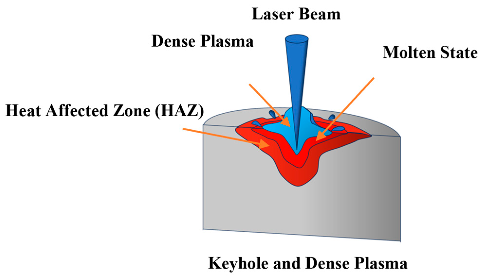
Figure 3 shows a diagram illustrating how the laser-ablated contact materials connect and interact. When the laser heats the material, it melts, and the molten metal flows out of the ablation crater, then starts to build up around the edges because of the way heat distributes. Since the heat is not perfectly even within the ablated area and the molten metal varies in thickness and viscosity, a small ridge forms around the molten ring. Some of the melted material spreads evenly across the surface, while other parts come together into tiny spherical blobs.
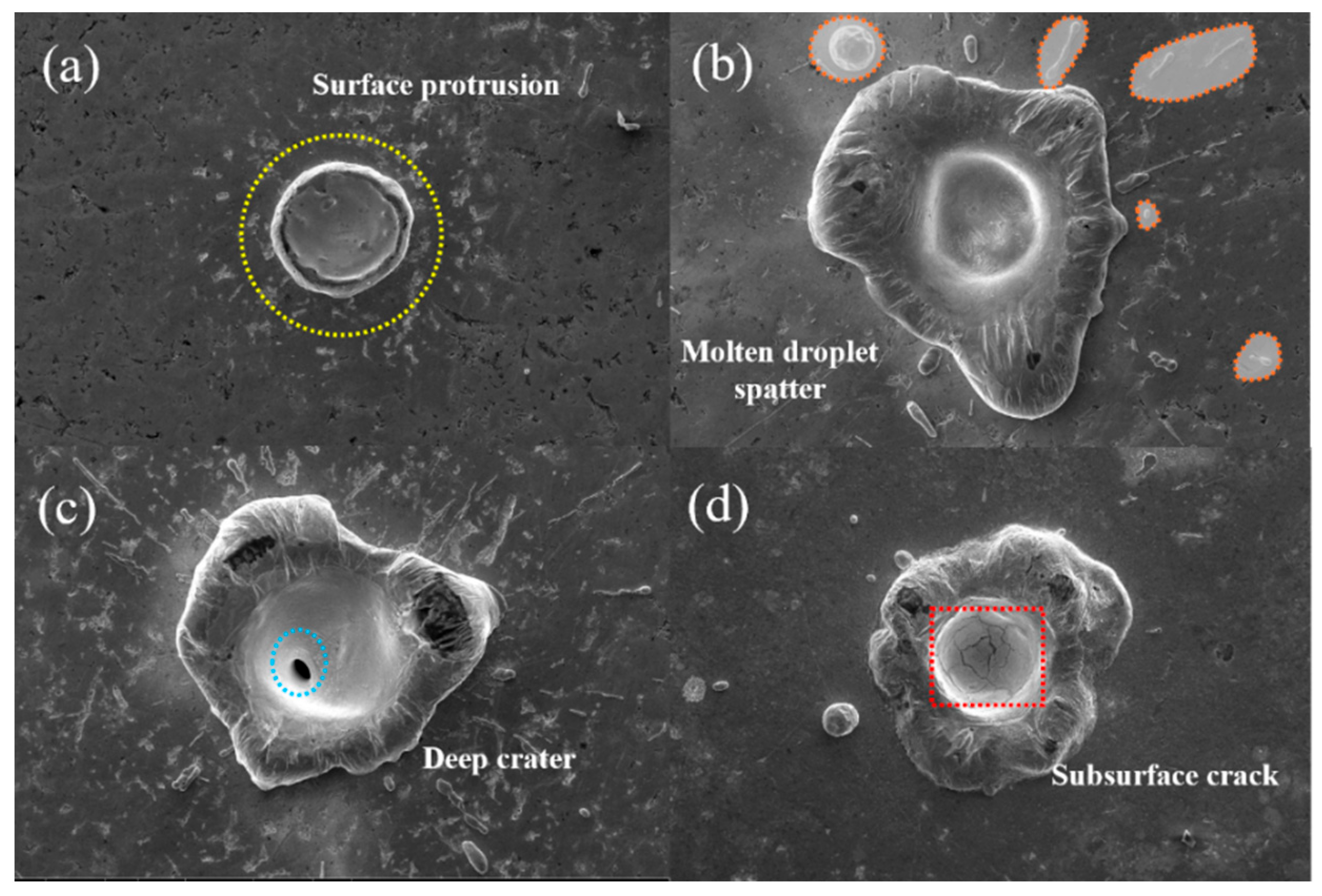
In the entire laser ablation process, the surface of the contact material develops various typical micro-topographical features, which you can see in Figure 4.
Figure 4a illustrates the convex hull structure formed on the AgNi10 material when exposed to a 500 W laser. At this stage, the laser energy causes intense high-temperature oxidation reactions on the surface. The higher the temperature and the more concentrated the energy in a particular area, the thicker the oxide layer becomes, leading to a relatively smooth, convex shape in the center. Around this area, a darker oxide zone appears along with clear circular boundaries, showing how heat affects the zone differently across the surface.
Figure 4b shows multiple spherical splashed particles around the edge of the ablation crater. This suggests that the surface temperature exceeded the melting point under laser irradiation, creating a molten pool. When the temperature increases, some molten metal breaks free from surface tension due to the kinetic energy released. These droplets splash out of the molten pool, cool down, and settle on the surface, creating the typical splash-like particles. This also results in a deeper ablation crater.
In Figure 4c, the ablation shape of AgNi10 under an 800 W laser is shown. The bottom of the crater is noticeably deeper, indicating that increasing the laser power results in more material being removed and causes more intense erosion.
Figure 4d illustrates that when the ablation duration is extended to 100 milliseconds, distinct grid-like cracks develop at the bottom of the crater. These cracks primarily result from the accumulation of thermal stress caused by prolonged heating. During the cooling phase, the release of these stresses leads to the formation of networked cracks, which may affect the structural stability of the contact surface. In high-energy laser ablation of metal electrical contact materials, changes in the ablation behavior are observed. The ablation mechanism is analyzed by examining the surface morphology and extracting key parameters from height data. The formulas and explanations for these measurement parameters are provided below:
(1) Ablation crater depth: This is the maximum vertical depression on the contact surface caused by melting, vaporization, and splashing after the laser is focused. The vertical distance of the ablative pit:
D e e p = L 0 L 1
(2) Linear ablation rate (μm/ms): As shown in Equation (3), this rate reflects the ablation deformation rate and retreat rate of the material, as well as the thermal conductivity change of the material under high-temperature ablation [25,26].
L A R = L 0 L 1 t
L 0 —The average height of the surface before ablation;
L 1 —The lowest point of the ablation pit on the surface after ablation;
t —Time of ablation (ms).
(3) The diameter-to-depth ratio of the ablation crater, shown in Equation (4), helps describe how the shape of the material changes as it is ablated. A smaller ratio means that the material mainly loses surface area without much loss of mass, which often indicates that the material is more resistant to ablation overall.
r d = R D e e p
Deep —Depth of ablation after the test;
R —The average diameter of the ablation pit on the sample surface.
(4) The growth rate of the ablation area (mm2/ms) describes how quickly the size of the area being melted or removed expands over time. It is calculated based on the diameter and area of the initial ablation spot, but it actually refers to the larger region that forms during ablation. Basically, if this area grows quickly, it means the material is not resisting lateral, or side-to-side, ablation very well.
R A = S S 0 t
S   —The ablation area of the contact material after testing;
S 0 —The contact material corresponds to the area of the ablation spot;
t —Time of ablation (ms).
The quantitative multi-parameter approach employed in this study provides systematic evaluation of ablation response through measurable parameters, such as ablation depth, linear ablation rate, and morphological characteristics. This deterministic quantitative analysis framework offers clear advantages in terms of reproducibility and direct correlation with material properties through established physical relationships. In the broader landscape of material damage assessment, parallel research developments have explored alternative analytical approaches. Recent studies have investigated soft computing methodologies and advanced signal processing techniques for material damage classification in composite systems, particularly addressing complex degradation patterns and delamination phenomena in CFRP materials [27]. These research directions, involving fuzzy logic systems, neural networks, and pattern recognition algorithms, represent complementary approaches that address different analytical challenges in material characterization. While such techniques tackle distinct methodological questions other than those addressed in the present quantitative framework, they contribute to the diverse methodological landscape in thermal damage evaluation and highlight potential avenues for future interdisciplinary research in comprehensive material assessment protocols.

3.1.3. Analysis of Ablation Resistance

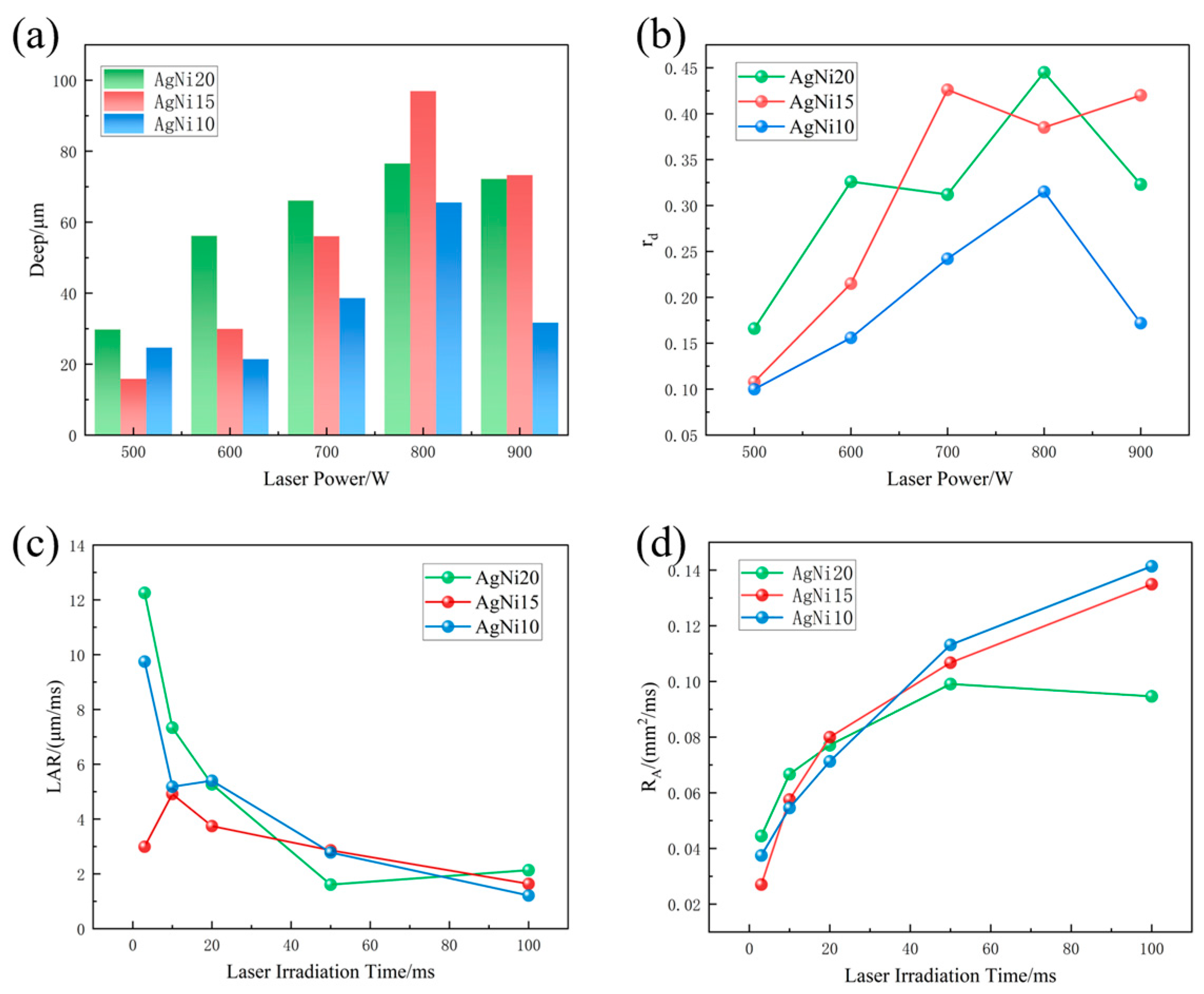
To comprehensively evaluate the ablation resistance response of silver-based contact materials with different Ni contents under laser thermal loading, this study quantitatively analyzes the thermal erosion behavior of three materials (AgNi10, AgNi15, and AgNi20) from the following four dimensions: longitudinal ablation depth, geometric characteristics of surface morphology, linear ablation rate, and ablation area growth rate. The statistical results of each index are shown in Figure 5.
In part (a), as laser power goes from 500 W to 900 W, all three materials show an increase in ablation depth, but their growth patterns and peak values differ quite a bit. AgNi10 keeps a low and steady ablation depth throughout, never exceeding about 70 μm, which shows that it is good at resisting deep thermal erosion along its length. On the other hand, AgNi20’s ablation depth jumps sharply at higher powers—especially above 700 W—and reaches nearly 100 μm at 800 W, showing that it is quite sensitive to laser energy. AgNi15 stays relatively stable at medium power but suddenly spikes in depth at 800 W, indicating that it might lack structural stability under intense heat.
For part (b), the diameter-to-depth ratio offers more insight into how the ablation shape differs. AgNi10 consistently has the lowest ratio, meaning its ablation mostly expands on the surface with less material loss, which is a good sign of resistance. For AgNi15 and AgNi20, the ratio fluctuates between 700 and 900 W. Notably, AgNi15’s ratio jumps to about 0.43 between 800 and 900 W, which suggests uneven lateral expansion and splash-like surface damage under high laser power, compromising surface integrity.
Part (c) looks at how quickly the material erodes over time (from 3 to 100 milliseconds). At the very start (3 ms), AgNi20 shows the highest ablation rate (around 12.26 mm/ms), meaning it suffers more damage quickly under short, intense laser pulses. Although AgNi10’s initial rate is also high, it decreases steadily over time, ending up at just over 1 mm/ms after 50 ms—setting it apart from other materials, with excellent thermal spreading and energy control. AgNi15 performs moderately but shows some rebound between 10 and 20 ms, indicating a delay in molten layer formation and less stable thermal behavior than AgNi10.
The graph in part (d) shows how the ablation area expands laterally over time. All three materials’ areas grow as time goes on, but AgNi10 and AgNi15 expand more steadily, reaching around 0.14 and 0.135 mm2/ms, respectively, by 100 ms, slightly higher than AgNi20. The latter’s area increases quickly at first but then slows down, likely due to uneven melting zones and reduced thermal response, which further points to weaker ablation resistance.
Overall, AgNi10 clearly outperforms the other materials; it has the shallowest ablation depth, most stable shape, slowest ablation rate, and most consistent lateral expansion. This shows that it handles thermal loads well and resists damage effectively. AgNi15 has acceptable performance under moderate heat but shows some instability when the laser power is high. AgNi20 consistently performs worse in multiple ways, easily forming deep craters, splashes, and uneven expansion, emphasizing its relatively poor resistance under laser irradiation.
The surface morphological analysis presented in this work provides direct insights into material thermal response behavior and ablation resistance characteristics through quantitative measurement and characterization of observable surface features resulting from laser ablation processes. The methodology is specifically designed to evaluate surface phenomena and their correlation with material properties under controlled thermal loading conditions.
However, comprehensive material degradation assessment requires consideration of both surface and subsurface phenomena, as fractures and cracks could also originate from internal defects, particularly under repeated stress conditions. Recent studies have demonstrated significant advances in subsurface defect characterization methodologies, including the adaptation of eddy current models for detecting and analyzing internal structural changes in composite materials. For instance, ref. [28] developed finite element analysis approaches based on energy functional methods for characterizing subsurface defects in CFRP plates, showing how internal defect evolution can be effectively monitored and predicted under cyclic loading conditions. These complementary research directions highlight the importance of integrated surface–subsurface analysis approaches for comprehensive material evaluation. While the present study maintains its focus on surface ablation characteristics and their quantitative analysis, the established surface parameters and morphological data could serve as valuable boundary conditions and validation benchmarks for future subsurface characterization studies. The evolution of subsurface defects under repeated thermal-mechanical stress represents a critical area for future investigation, where the integration of surface morphological analysis with advanced subsurface detection techniques such as eddy current testing could provide a more complete understanding of material degradation mechanisms. Such integrated approaches would enhance the predictive capability of material performance assessment and represent important directions for future developments of the methodology.

3.2. Results of Ablation Resistance of Contact Materials Under Actual Electrical Contact Test Conditions

To verify the accuracy of the ablation resistance analysis results after laser ablation, electrical contact tests under different current gradient levels were conducted on the three materials. The specific test scheme is shown in Table 3.
Mass loss, microscopic morphological characteristics, and surface roughness of the electrical contact materials were measured under identical conditions to quantitatively and qualitatively compare the ablation resistance of AgNi10, AgNi15, and AgNi20 silver-based contact materials.
m = m 1   m 0
The mass loss is calculated as the difference between the mass of the contact measured before and after the test.
The microstructural characteristics of the contact surface are generally quantified using roughness parameters. In practical industrial applications, the most frequently used 3D parameters among height parameters include the arithmetic mean height ( S a ), root mean square height ( S q ), maximum height ( S z ), skewness ( S s k ), and kurtosis ( S k u ) [29]. Among these, S a , S z , and S k u , respectively, characterize the dispersion of the surface height distribution, the symmetry of the height distribution, and the sharpness of surface undulations, and they are often used in combination for surface morphology characterization [30,31]. The 3D surface roughness parameters are calculated in accordance with the ISO 25178 standard [32]:
Arithmetic mean height ( S a ): The arithmetic mean of the absolute values of the heights of all points on the surface profile, which characterizes the average dispersion degree of the overall surface undulations. A smaller value indicates a smoother surface.
S a = 1 N [ i = 1 m j = 1 n | Z x i , y i | ]
In the formula, S a is the sum of sampling points; m and n are the dimensions of the sampling area, and Z ( x i , y i ) is the difference between the height value of the sampling point ( x , y ) and the average height value of the surface.
Maximum surface height S z : The sum of the height of the maximum peak height and the maximum valley depth within the sampling area.
S z = S p + S v
Surface kurtosis ( S k u ): A parameter that characterizes the sharpness of peak and valley shapes within the sampled area. A larger value indicates more peaks or higher peak heights on the surface.
S ku = 1 S q 4 [ 1 N i = 1 m j = 1 n Z ( x i , y i ) 4 ]
Figure 6 illustrates how the 3D surface roughness parameters change over time on materials with different amounts of Ni after undergoing electrical contact tests. The data show that the Sa values do not vary much across different test conditions, which means that the overall surface roughness stays fairly consistent during arc ablation without big spikes or drops.
When looking at two key indicators that measure extreme surface features— S z and S k u —there are clear differences between the materials. AgNi10 and AgNi15 tend to stay quite stable, showing only small changes in surface shape, which suggests that they are fairly resistant to damage. Specifically, AgNi10 changes very gradually across different current levels, pointing to good uniformity in resisting ablation. On the other hand, as the current goes up from 10 A to 50 A, the S z and S k u values for AgNi20 rise sharply—more than doubling in some cases—indicating that this material is more likely to develop deep craters and sharp bumps when subjected to high-energy arc impacts.
This behavior can be linked to uneven melting and re-solidification happening locally in the high-Ni alloy under the combined effects of intense heat and electrical stress. This process tends to make the microstructure less stable, which explains why the material’s resistance to arc erosion drops considerably at higher currents.
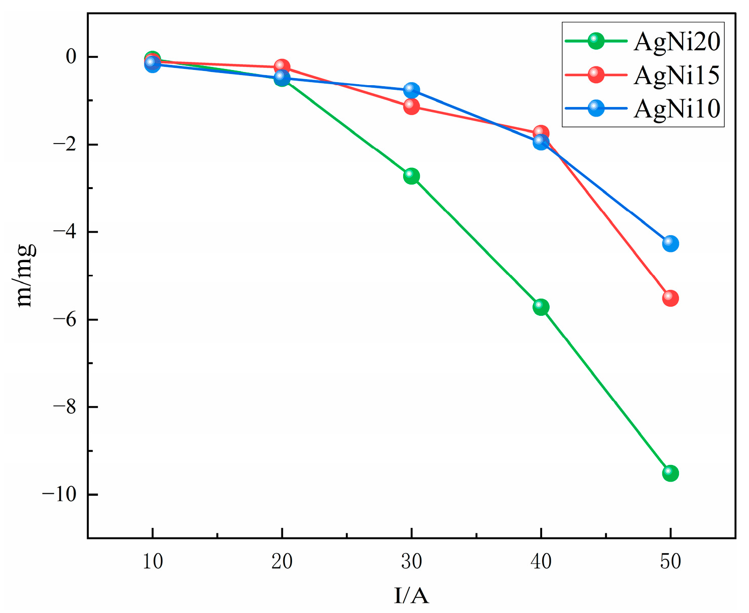
To intuitively quantify the surface ablation effects of different materials, a comparative analysis of mass loss for each material under various current levels was conducted. The data in Figure 7 shows that, within the current range of 10 A to 50 A, the mass loss of AgNi10, AgNi15, and AgNi20 exhibits an increasing trend with significant composition dependence. Specifically, AgNi10 has the lowest overall mass loss, which increases approximately linearly with the current, indicating good stability in ablation resistance. AgNi15 experiences a sudden increase in mass loss in the medium-to-high current range (30–50 A), suggesting a decline in its thermal stability under high current-carrying conditions. AgNi20 performs the worst, with a sharp rise in mass loss when the current exceeds 20 A, reaching a maximum loss of 9.52 mg, reflecting its high sensitivity to arc ablation. These differences reveal the intrinsic distinctions in the thermal–mechanical response mechanisms of materials with different Ni contents under arc action. The mass loss patterns of the materials are closely related to their microstructures, thermophysical properties, and phase transformation behaviors in high-temperature arc environments.
To gain a clearer understanding of the ablation resistance exhibited by the AgNi series materials under intense arc impacts, SEM micrographs of the contact surfaces after operation at 50 A were analyzed, as Figure 8 shows. As Figure 8a,d shows, the surfaces of AgNi10 moving and stationary contacts display only a few micro-pores, and the overall contour remains smooth, without major cracks or traces of ablation. This suggests that AgNi10 maintains good structural integrity even under high current conditions. In contrast, the surfaces of AgNi15 visible in Figure 8b,e feature numerous dense micro-pores and slight bulging in some regions, indicating localized melting, vaporization, and re-solidification caused by the high arc temperature. These effects reduce thermal stability in micro-areas, leading to weaker ablation resistance compared to AgNi10. Most notably, AgNi20, as Figure 8c,f depicts, displays clear cracks on the moving contact surface, along with larger pores and more severe structural damage. Although the stationary contact remains relatively flat, it still shows obvious ablation pits. This pattern reflects that higher nickel content materials often have limited capacity to dissipate thermal stresses under high currents, making them more prone to crack propagation and material spalling during ablation.
Overall, the analysis emphasizes that, while AgNi20 is most susceptible to thermal damage during arc exposure, AgNi10 demonstrates the most stable electro-thermal performance with minimal surface erosion, showing excellent ablation resistance. AgNi15’s performance falls somewhere in between.

4. Analysis of Changes in Thermal Effects on the Surface of Contact Materials

Comparison of the results from both experiments shows full consistency in the conclusions regarding the ablation resistance of the contacts. Specifically, the insights gained from analyzing both the longitudinal and transverse dimensions during laser ablation under different power levels and durations align perfectly with the findings from tests conducted at various current levels in electrical contact scenarios. This consistency suggests that, within the current laser testing framework, there is a strong positive correlation between how the contact surface responds thermally to laser exposure and how it reacts to arc erosion during actual electrical operation. These results confirm that laser ablation is an effective and swift method for assessing contact material behavior.
To gain a deeper understanding of the thermal response characteristics under both testing methods, this study employs a multi-scale parameter known as the surface fractal dimension. This approach helps reveal the intrinsic patterns in how contact materials change thermally.
Rooted in fractal geometry, the fractal theory-based characterization model uses the concept of self-similarity across multiple scales [33,34]. The fractal dimension, D is a quantitative measure of surface complexity, capturing multi-scale surface features without being limited by measurement precision. It offers a comprehensive perspective on surface morphology, making it a valuable tool for detailed analysis of material surfaces [35,36]. In this study, the box-counting method was used to calculate the fractal dimension D , with the following formula:
D = lim ε 0 [ l o g N ( ε ) / l o g ( 1 / ε ) ]
Following laser ablation and electrical contact tests, the fractal dimensions of the contact surfaces were calculated using the box-counting method. The results are presented in Figure 9 and Figure 10 separately. Figure 9 illustrates the evolution of fractal surface patterns for AgNi10 contacts under varying laser power settings. It shows that increasing laser power leads to more pronounced changes in the fractal surface and a gradual increase in surface roughness. Figure 10 depicts the fractal surface changes of AgNi10 contacts under different electrical contact current conditions, revealing a similar trend of increasing surface complexity with higher current. These observations indicate that, regardless of the heat source input, the contact surface responds to both laser and electrical energy in a comparable manner. Overall, this confirms the intrinsic consistency between the two testing methods.
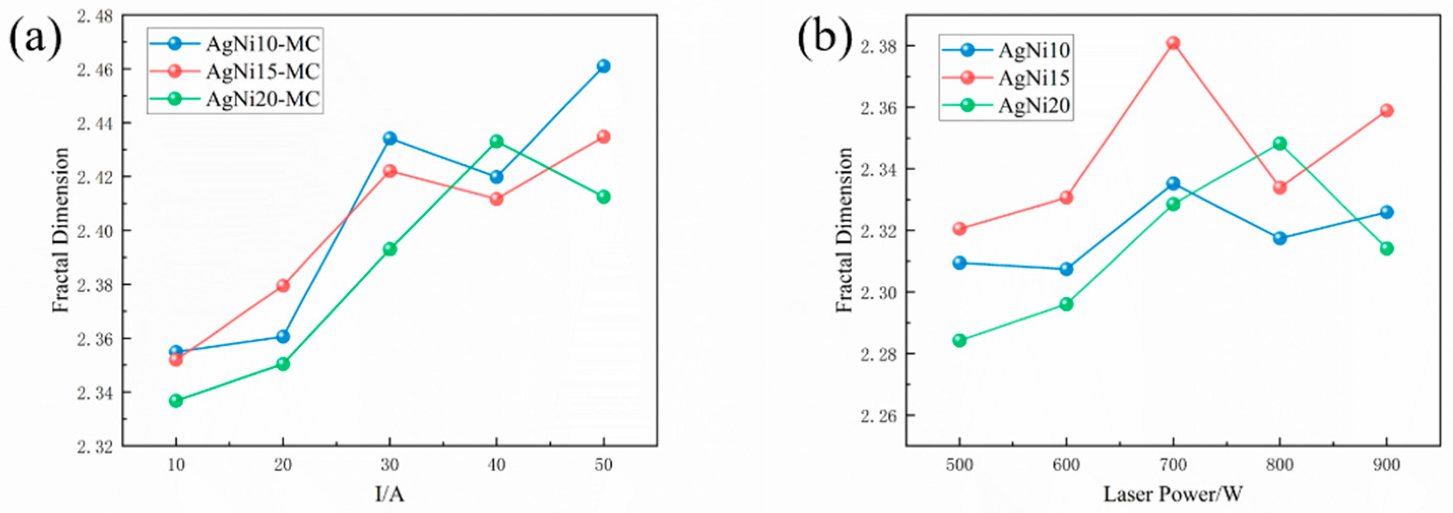
To quantify the evolution law of material surface complexity, the fractal dimension D of the fractal surfaces of different materials was calculated, and the results are shown in Figure 11. With the increase of energy input, the fractal dimensions obtained by both laser ablation and arc ablation tests show an increasing trend, and their variation patterns are highly consistent, indicating that the evolution of material surface complexity under the action of the two heat sources follows similar physical mechanisms.
Furthermore, the Pearson correlation coefficients of the fractal dimensions obtained by the two methods under different test conditions were calculated (could be seen in Table 4) to quantitatively evaluate their correlation. The correlation coefficients are close to 1, demonstrating that the laser ablation and arc ablation methods have high consistency and good comparability in evaluating surface morphological characteristics.
Table 4 presents the Pearson correlation coefficients between the surface fractal dimensions of AgNi materials with different Ni contents under laser ablation and electrical contact tests. Overall, all three groups of materials exhibit good linear correlation, with correlation coefficients exceeding 0.78, which confirms the high consistency between the two testing methods. A detailed analysis of the correlation performance of each material is as follows: AgNi20 shows the highest correlation coefficient, reaching 0.9201, indicating that the variation trends of its fractal dimensions under the action of two different heat sources are almost completely synchronized; AgNi15 has a moderate correlation coefficient of 0.7884; and AgNi10 has a correlation coefficient of 0.8467, slightly higher than that of AgNi15.
The results of this study indicate that the high consistency in the evolution of material surface morphology between laser ablation and arc ablation reflects the similar physical mechanisms in the thermal erosion process of materials under the action of the two heat sources. Through concentrated and controllable thermal input, laser ablation induces melting, vaporization, and re-solidification on the material surface, forming complex multi-scale morphological structures. This shows a high degree of similarity to the local high-temperature ablation process caused by arcs in electrical contact tests in terms of energy transfer and material response. As a quantitative index for multi-scale self-similar features, the fractal dimension not only effectively captures the evolution of surface roughness but also reveals the energy dissipation law of materials under different thermal loads.
The enhancement of current laser ablation platform reliability necessitates integration with emerging digital modeling frameworks. Recent advancements in AI-assisted thermal modeling and finite element simulation (FEM) have demonstrated significant potential for predicting thermomechanical behaviors under high-energy inputs, including deformation, stress accumulation, and material failure [37]. Moving forward, coupling experimental ablation results with AI-enhanced FEM models may pave the way for a hybrid analytical framework that not only characterizes surface morphological features but also predicts internal thermal evolution and subsurface damage. This integrated approach would substantially improve early-stage material screening efficiency and accelerate engineering design optimization. Table 5 presents a systematic comparison between laser-based approaches and AI-enhanced real-time electrical monitoring platforms [38], illustrating their characteristic differences as complementary technological approaches within the broader landscape of intelligent diagnostic systems.
The comparative analysis reveals distinct yet complementary monitoring modalities—thermal morphology analysis versus electrical signal monitoring—with both approaches demonstrating efficacy in rapid material state evaluation. While laser ablation testing exhibits certain limitations in precisely replicating electrical contact ablation phenomena (particularly regarding heat source morphology characteristics), the established high correlation validates its reliability for rapid screening and preliminary assessment. Future developments may integrate real-time signal acquisition and AI-based interpretation with laser-based platforms, potentially yielding multimodal diagnostic systems capable of concurrent surface damage characterization and electrical integrity evaluation. Such technological convergence, when combined with enhanced characterization methodologies, could provide deeper mechanistic insights into material thermal erosion processes, thereby significantly advancing both the methodological applicability in materials engineering and the development of high-performance electrical contact materials.

5. Conclusions

This study focuses on AgNi series silver-based contact materials, proposing and systematically verifying a rapid testing method for erosion resistance performance based on laser ablation while conducting a multidimensional comparison with traditional electrical contact test results. The main conclusions are as follows.
(1) The test results based on the laser ablation testing platform indicate that, under fixed parameter conditions, the variation coefficients of ablation pit diameters for the three materials, AgNi10, AgNi15, and AgNi20, are all below 4%, and the relative difference in average diameter for each group does not exceed 1.25%, thereby verifying the excellent repeatability and process stability of this method. Through systematic testing of AgNi series contact materials under different energy input conditions, typical characteristics of the surface micro-morphology were obtained, including convex structures, spherical splashed particles, deep ablation pits, and mesh-like cracks. These features reveal the microstructural responses and morphological evolution patterns of the materials under the effects of high-temperature laser ablation, providing a reliable foundation for a deeper understanding of the ablation mechanisms and failure behaviors of contact materials.
(2) By systematically analyzing the multi-dimensional parameters, such as ablation depth, diameter-depth ratio, linear ablation rate, and ablation area growth rate, the thermal erosion behavior of contact materials with different Ni contents (AgNi10, AgNi15, and AgNi20) under laser thermal loading was clarified. The experimental results show that AgNi10 exhibits a shallow ablation depth, a small diameter-to-depth ratio, a lower linear ablation rate, and a more uniform ablation area expansion, showing excellent ablation resistance. AgNi20 presents deep ablation pits, significant surface damage and structural failure, and weak ablation resistance. AgNi15’s performance is between that of the other two materials.
(3) Comparing the multi-dimensional parameter analysis results of laser ablation and the electrical contact test, it is found that the two methods show a high degree of consistency in the regularity of thermal erosion behavior and the analysis results of ablation resistance of materials. Fractal dimension analysis shows that, with the increase of laser power or electrical contact current, the surface roughness and morphological complexity show an increasing trend, indicating that the thermal erosion response of materials under different energy inputs has a consistent physical mechanism. This agreement was further quantified by Pearson correlation coefficient analysis, with correlation coefficients of 0.8467, 0.7884, and 0.9201 for AgNi10, AgNi15, and AgNi20, all higher than 0.78, confirming the equivalence of the two methods in characterizing ablation resistance.
Although distinct differences exist between laser ablation and arc erosion in terms of thermal source characteristics, energy distribution, and action mechanisms, laser ablation demonstrates significant advantages for rapid quantitative evaluation of ablation resistance due to its controllable energy input and uniform thermal field distribution. However, its applicability under extreme service conditions requires further validation. Through multiscale fractal analysis and correlation verification, this study establishes a scientific foundation for employing laser ablation testing as an effective tool for high-throughput screening and performance prediction of contact materials. The findings provide critical references for optimizing electrical contact material design and enhancing the reliability of electrical components.

Author Contributions

Conceptualization, W.L. and Y.W.; methodology, Y.W. and L.L.; validation, L.L. and M.L.; formal analysis, Y.W., L.L., B.J. and Y.J.; investigation, R.M. and S.M.; resources, X.Z. and T.L.; data curation, Y.W.; writing—original draft, Y.W.; writing—review and editing, Y.W. and L.L.; supervision, W.L.; project administration, Y.W.; funding acquisition, W.L. All authors have read and agreed to the published version of the manuscript.

Funding

This research was funded by the Key Research and Development Program of Shijia-zhuang Universities in Hebei (241130161A) and the Continuation Funding Project for Innovative Research Groups of Natural Science Foundation of Hebei Province (E2024202298).

Institutional Review Board Statement

Not applicable.

Informed Consent Statement

Not applicable.

Data Availability Statement

The data presented in this study are available upon request from the corresponding author due to confidentiality restrictions.

Conflicts of Interest

All authors declare that the research was conducted in the absence of any commercial or financial relationships that could be construed as a potential conflict of interest.

References

  1. Pan, J.; Zhang, W.; Zhang, L.B.; He, Q.; Chen, W. Vibration Reliability Test Assessment of Electrical Connector Contacts. J. Mech. Eng. 2021, 57, 257–266. [Google Scholar]
  2. Yu, C.M.; Dong, W.J.; Lu, K.F.; Li, X.; Li, R.; Ge, Y. Analysis of flexibility requirements and key technologies for aerospace control systems. Aerosp. Control 2025, 43, 1–7. [Google Scholar]
  3. Zhang, P.; Guo, B.; Zhou, S.; Zhang, Z.; Li, W. Study on sliding wear characteristics of tungsten carbide particle reinforced copper matrix composites under electrical contact. Tribol. Trans. 2023, 66, 292–301. [Google Scholar] [CrossRef]
  4. Chen, G.; Zhao, W.; Wen, S.; Liu, X. Three dimensional graphene/copper dual networks as composite conductors with enhanced current carrying capacity. ACS Appl. Nano Mater. 2024, 7, 8164–8174. [Google Scholar] [CrossRef]
  5. Ma, G.; Wang, D.; Liu, Z.; Bi, S.; Zan, Y.; Xiao, B.; Ma, Z. Effect of hot pressing temperature on microstructure and tensile properties of SiC/Al-Zn-Mg-Cu composites. Acta Met. Metall. Sin. 2019, 55, 1319–1328. [Google Scholar]
  6. Zhai, G.F.; Cui, X.L.; Yang, W.Y. Review on the development of electromagnetic relay products and research technologies. Electr. Energy Manag. Technol. 2016, 2, 1–8. [Google Scholar]
  7. Volm, D.; Winkler, F. Development of a compact relay for high voltage switching of up to 1000V and 40A. In Proceedings of the 27th International Conference on Electrical Contacts ICEC 2014, Dresden, Germany, 22–26 June 2014; VDE: Frankfurt am Main, Germany, 2014; pp. 1–5. [Google Scholar]
  8. Wang, H.; Cai, Q.; Wang, J.; Zhang, Y.; Hu, D.; Wang, Y. First-principles and experimental investigations on physical properties and arc erosion behavior of metal-doped AgSnO2 electrical contact materials. Ceram. Int. 2023, 49, 26033–26048. [Google Scholar] [CrossRef]
  9. Fei, Y.; Wang, X.; Zhao, N.; Li, H.; Li, H.; Qiu, Y. Enhanced arc erosion and dynamic welding resistance of Ag-10 wt% Ni@ Gr contact material. Ceram. Int. 2024, 50, 21989–22000. [Google Scholar] [CrossRef]
  10. Gao, J.F.; He, S.; Xia, Y.; Ding, Y.; Wang, K.; Long, Y.; Ruan, W.; Duan, M.; Pang, Z. Research and application progress of silver-based contact materials for low-voltage electrical appliances. J. Funct. Mater. 2024, 55, 6053–6061. [Google Scholar]
  11. Yuan, X.; Fu, F.; He, R. Graphene-enhanced silver composites for electrical contacts: A review. J. Mater. Sci. 2024, 59, 3762–3779. [Google Scholar] [CrossRef]
  12. Huang, R.; Qiong, W.U.; Meng, Y. Influence of operation number on arc erosion behavior of Ag/Ni electrical contact materials. Trans. Nonferrous Met. Soc. China 2022, 32, 2681–2695. [Google Scholar] [CrossRef]
  13. Guo, Y. Progress in Cu_based Contact Materials of Low Voltage Apparatus. Electr. Eng. Mater. 2011, 3, 10–13. [Google Scholar]
  14. Sexton, L.; Lavin, S.; Byrne, G.; Kennedy, A. Laser cladding of aerospace materials. J. Mater. Process. Technol. 2002, 122, 63–68. [Google Scholar] [CrossRef]
  15. Mi, G.; Xiong, L.; Wang, C.; Hu, X.; Wei, Y. A thermal-metallurgical-mechanical model for laser welding Q235 steel. J. Mater. Process. Technol. 2016, 238, 39–48. [Google Scholar] [CrossRef]
  16. Shanmugarajan, B.; Sathiya, P.; Buvanashekaran, G. Mechanical and metallurgical properties of autogenous laser welded P92 material. J. Manuf. Process. 2016, 24, 11–18. [Google Scholar] [CrossRef]
  17. Ma, C.; Gu, D.; Dai, D.; Zhang, H.; Zhang, H.; Yang, J.; Guo, M.; Du, Y.; Gao, J. Microstructure evolution and high-temperature oxidation behaviour of selective laser melted TiC/TiAl composites. Surf. Coat. Technol. 2019, 375, 534–543. [Google Scholar] [CrossRef]
  18. Liu, S.; Sun, Q.; Wang, J.; Guo, M.; Hou, H. Exploration of the influence mechanism of La doping on the arc erosion resistance of Ag/SnO2 contact materials by a laser-simulated arc. J. Mater. Eng. Perform. 2021, 30, 7577–7583. [Google Scholar] [CrossRef]
  19. Liu, S.; Sun, Q.; Wang, J.; Hou, H. How Cu doping improves the interfacial wettability between Ag and SnO2 of Ag/SnO2 contact material. J. Alloys Compd. 2019, 792, 1248–1254. [Google Scholar] [CrossRef]
  20. Wang, J.; Zhao, H.; Wang, J.; Fu, C.; Chang, Y. Effect of CuO additives on the formation of SnO2-rich layers in Ag-SnO2 materials. J. Alloys Compd. 2019, 770, 920–925. [Google Scholar] [CrossRef]
  21. Dong, B.W.; Wu, Z.P.; Jie, J.C.; Kang, H.J.; Li, T.J. Study on microstructure and anti-ablation mechanism of Cu-W alloy for electrical contacts. Copp. Eng. 2023, 4, 63–70. [Google Scholar]
  22. Pech, M.; Vrchota, J.; Bednář, J. Predictive maintenance and intelligent sensors in smart factory. Sensors 2021, 21, 1470. [Google Scholar] [CrossRef]
  23. Mohanty, A.; Mohanty, S.K.; Mohapatra, A.G. Real-time monitoring and fault detection in AI-enhanced wastewater treatment systems. In The AI Cleanse: Transforming Wastewater Treatment Through Artificial Intelligence: Harnessing Data-Driven Solutions; Springer: Berlin/Heidelberg, Germany, 2024; pp. 165–199. [Google Scholar]
  24. Haque, R.; Bajwa, A.; Siddiqui, N.A.; Ahmed, I. Predictive Maintenance in Industrial Automation: A Systematic Review of IOT Sensor Technologies and AI Algorithms. Am. J. Interdiscip. Stud. 2024, 5, 1–30. [Google Scholar] [CrossRef]
  25. Wang, H.; Wen, Q.L.; Huang, H.; Huang, G.; Jiang, F.; Lu, J.; Wu, X. Study on ablation characteristics and mechanism of CVD single crystal diamond processed by femtosecond laser. Acta Photonica Sin. 2023, 52, 51–65. [Google Scholar]
  26. Maddu, S.; Srivastava, T.; Katari, N.K.; Merugu, K.; Gundla, R.; Krishna Mohan, S. Studies on ablative performance of silicone low-density ablative material. Silicon 2023, 15, 3599–3608. [Google Scholar] [CrossRef]
  27. Tavares, A.; Di Lorenzo, E.; Cornelis, B.; Peeters, B.; Desmet, W.; Gryllias, K. Machine Learning approaches to damage detection in composite structures combining experimental and simulation domains. Mech. Syst. Signal Process. 2024, 215, 111412. [Google Scholar] [CrossRef]
  28. Versaci, M.; Laganà, F.; Morabito, F.C.; Palumbo, A.; Angiulli, G. Adaptation of an Eddy Current Model for Characterizing Subsurface Defects in CFRP Plates Using FEM Analysis Based on Energy Functional. Mathematics 2024, 12, 2854. [Google Scholar] [CrossRef]
  29. Sztankovics, I. Preliminary study on the function-defining 3D surface roughness parameters in tangential turning. Int. J. Integr. Eng. 2023, 15, 72–81. [Google Scholar] [CrossRef]
  30. Wang, C.; Yong, R.; Luo, Z.; Du, S.; Karakus, M.; Huang, C. A novel method for determining the three-dimensional roughness of rock joints based on profile slices. Rock. Mech. Rock. Eng. 2023, 56, 4303–4327. [Google Scholar] [CrossRef]
  31. Zhou, F.F.; Yin, N.; Wu, Z.S.; Song, S.Y.; Ju, P.F.; Zhang, Z.N. Research Progress on Electrical Contact Performance Based on Rough Surface Feature Analysis. China Surface Engineering. pp. 1–24. Available online: https://link.cnki.net/urlid/11.3905.tg.20250321.1101.004 (accessed on 11 August 2025).
  32. GB/T 33523.2-2017; Geometrical Product Specifications (GPS)—Surface Texture: Areal—Part 2: Terms, Definitions and Surface Texture Parameters. China Standards Press: Beijing, China, 2017.
  33. Huang, J.; Zhou, Y.; Luo, Y. Representing topological self-similarity using fractal feature maps for accurate segmentation of tubular structures. In Proceedings of the European Conference on Computer Vision, Milan, Italy, 29 September–4 October 2024; Springer: Berlin/Heidelberg, Germany, 2024; pp. 143–160. [Google Scholar]
  34. Guida, G.; Viggiani, G.M.B.; Casini, F. Multi-scale morphological descriptors from the fractal analysis of particle contour. Acta Geotech. 2020, 15, 1067–1080. [Google Scholar] [CrossRef]
  35. Bian, L. Multiscale nature of spatial data in scaling up environmental models. In Scale in Remote Sensing and GIS; Routledge: Abingdon-on-Thames, UK, 2023; pp. 13–26. [Google Scholar]
  36. Rancu, A.; Chen, C.X.; Price, H.; Wax, A. Multiscale optical phase fluctuations link disorder strength and fractal dimension of cell structure. Biophys. J. 2023, 122, 1390–1399. [Google Scholar] [CrossRef]
  37. Maduabuchi, C. Thermo-mechanical optimization of thermoelectric generators using deep learning artificial intelligence algorithms fed with verified finite element simulation data. Appl. Energy 2022, 315, 118943. [Google Scholar] [CrossRef]
  38. Pratticò, D.; Laganà, F.; Oliva, G.; Fiorillo, A.S.; Pullano, S.A.; Calcagno, S.; De Carlo, D.; La Foresta, F. Integration of LSTM and U-Net models for monitoring electrical absorption with a system of sensors and electronic circuits. IEEE Trans. Instrum. Meas. 2025, 74, 2533311. [Google Scholar] [CrossRef]
Figure 1. Schematic diagram of laser ablation equipment.
Applsci 15 08961 g001
Figure 2. Repeatability test results: (a) AgNi10 repeatability effect; (b) AgNi15 repeatability; (c) AgNi20 reproducibility effect.
Applsci 15 08961 g002
Figure 3. Diagram of the coupling effect of laser ablation contact materials.
Applsci 15 08961 g003
Figure 4. Microscopic characteristics of the surface of laser ablation contacts: (a) Surface protrusion; (b) Molten droplet spatter; (c) Deep crater; (d) Subsurface crack.
Applsci 15 08961 g004
Figure 5. Comparison of how different ablation resistance parameters behave under laser power changes: (a) D e e p ; (b) r d ; (c) L A R ; (d) R A .
Applsci 15 08961 g005
Figure 6. Calculation results of 3D roughness parameters: (a) S a ; (b) S z ; (c) S k u .
Applsci 15 08961 g006
Figure 7. Electrical contact mass loss curve.
Applsci 15 08961 g007
Figure 8. The microscopic morphology of the surface of the AgNi contacts after action is as follows: (a) AgNi10 contacts, (b) AgNi15 contacts, (c) AgNi20 contacts, (d) AgNi10 static contacts, (e) AgNi15 static contacts, (f) AgNi20 static contacts.
Applsci 15 08961 g008
Figure 9. AgNi10 surface fractal surface at different powers: (a) 500 W; (b) 600 W; (c) 700 W; (d) 800 W; (e) 900 W.
Applsci 15 08961 g009
Figure 10. AgNi10 surface fractal surface at different current levels: (a) 10 A; (b) 20 A; (c) 30 A; (d) 40 A; (e) 50 A.
Applsci 15 08961 g010
Figure 11. Results of fractal dimension calculation: (a) Fractal dimension (FD) under different currents in electrical contact tests; (b) Fractal dimension (FD) under different powers in laser tests.
Applsci 15 08961 g011
Table 1. Laser ablation test scheme.
Test SampleSpecification ComparisonTest ConditionsTest Name
Variable PowerTimes Change
AgNi10/Cu
AgNi15/Cu
AgNi20/Cu
Applsci 15 08961 i001Laser Power/W500, 600, 700, 800, 900600
Action Time/ms33, 10, 20,
50, 100
Diameter of light spot/mm0.195
Table 2. Comparison table of repeatability of laser ablation test.
Contact MaterialAverage Diameter
(μm)
C V (%)
AgNi1081.003.78
AgNi1579.003.98
AgNi2084.002.56
Table 3. Electrical contact test scheme.
Test ConditionsTest Parameters
Test VoltageAC 220 V
Test Current10 A, 20 A, 30 A, 40 A, 50 A
Movements’ Num.3000 times
Contact Pressure1.5 N
Test MethodOpen & Close Experiment
Connection Time1 s
Breaking Distance2 mm
Table 4. Pearson correlation coefficient table.
Test SampleAgNi10AgNi15AgNi20
r0.84670.78840.9201
Table 5. Comparison of laser ablation and AI monitoring platforms.
Comparison DimensionLaser Ablation-Based MethodAI-Enhanced Embedded Monitoring
Main Stimulus InputPulsed laser (thermal excitation)Electrical load (voltage/current)
Diagnostic FocusSurface morphology evolution (cracks, roughness)Electrical absorption dynamics
Output ParametersDepth, ablation rate, fractal dimension, areaImpedance, signal waveform, transient voltage/current
Analysis MethodologyStatistical + morphology feature extractionLSTM + U-Net deep learning pipeline
Instrumentation RequiredLaser, SEM, profilometer, IR cameraEmbedded sensors, ADCs, microcontrollers
Temporal ResolutionPost-process, quasi-staticReal-time
Main Application ScenarioMaterial screening under thermal loadPredictive maintenance, fault detection
Core AdvantageControlled energy input, clear surface evolutionHigh sensitivity to electrical behavior
Integration PotentialExpandable to multi-modal sensor systemsCompatible with broader sensing ecosystems
Disclaimer/Publisher’s Note: The statements, opinions and data contained in all publications are solely those of the individual author(s) and contributor(s) and not of MDPI and/or the editor(s). MDPI and/or the editor(s) disclaim responsibility for any injury to people or property resulting from any ideas, methods, instructions or products referred to in the content.