1. Introduction
Today’s advanced electronic components and power semiconductors bring new challenges for designing and developing power electronics systems. Advancements in power electronics are closely tied to progress in materials science. Wide-bandgap semiconductors, especially gallium nitride (GaN) and silicon carbide (SiC), are at the forefront of current research due to their superior electron mobility and high breakdown voltage capabilities. The Google Little Box Challenge showcased the reliable performance of GaN transistors [
1,
2]. These materials have made it possible to create fast-switching, high-voltage devices that are already being used successfully. However, some areas, like low-voltage direct current systems, are still not widely used in real-world applications. Even today, GaN transistors are not widely used in the industry and are mostly found in specific products like phone chargers. To make DC technologies more practical, especially those working at higher voltages, they still need to become smaller, more efficient, more reliable, and cheaper for use in many different applications.
However, the use of advanced semiconductors along with high switching frequencies remains popular for niche applications. In this context, it is important to consider the new electrical infrastructure that is already being implemented in several European countries. For new buildings, several scenarios are possible: coexistence with the traditional AC grid (hybrid systems), the use of a separate DC grid, or the continuation of the conventional AC grid [
3,
4]. To manage power flow between these grids, a high-level smart control system must be developed. This task is further complicated by the need to simultaneously supply both DC loads, which represent the majority of household devices, and AC loads, which are still necessary for high-power appliances such as washing machines and refrigerators. At the same time, renewable energy sources will require intelligent control systems to efficiently manage power distribution and maximize building energy performance. Some devices have already been developed to address these challenges [
5,
6]. Additionally, the decentralization of electrical systems is an increasingly relevant topic. A notable example is the recent blackout in Spain, which highlighted the advantages of decentralized systems that can continue supplying electricity to buildings even when disconnected from the main AC grid [
7]. Power electronics for renewable energy sources are well-studied and have been developed and tested in various research works [
8,
9,
10,
11]. However, there is still space for improvement in terms of reducing the size, weight, and cost of these systems.
To cover this issue, some other applications can be taken into account. For example, wireless power transfer (WPT) is still facing big challenges in its development [
12,
13,
14,
15]. The design of mutual inductances for WPT is also important, and to reach the necessary inductance value, the layered double D coil can be used [
16]. The main issues are its energy losses and high cost, which make it less suitable for high-power use. To make the systems smaller, higher switching frequencies are needed. However, because of strict rules, WPT can only operate in a limited switching frequency range, which creates extra technical difficulties. Still, working within this frequency range can lead to big improvements in making power electronics smaller, cheaper, and more compact. Researchers are still exploring new circuit designs, but using such high frequencies also brings new and complex engineering problems.
Power electronics is moving more and more toward high-power-density converters, leading to the idea of “on-chip” power electronics [
17]. Often, making devices smaller and lighter also helps reduce costs, especially as the technology improves and can be produced in large quantities. However, studies show that just making better switches is not enough to greatly increase power density or efficiency [
18]. A major challenge comes from ferrite-based magnetic parts, which cause a lot of energy loss and make it hard to raise switching frequencies above 500 kHz. Even though there has been progress in lowering magnetic losses, future designs will need to reduce or even remove magnetic components altogether. One of the promising solutions is to avoid cores and make air core inductances and transformers, as shown in [
19,
20]. High-frequency converters have been built [
21,
22,
23], but they are still not suitable for high-power applications. A very interesting and prospective solution is planar inductances or transformers for power electronics [
24,
25]. At the same time, integrating an inductance into a printed circuit board (PCB) is a possible approach to reach high power density [
26,
27,
28,
29]. In this context, accounting for the proximity effect is essential to maintain high efficiency, especially at high frequencies where AC losses become significant [
30].
However, recently, a lot of works have been presented to cover only very low power applications, where integrated PCB inductances are used [
31,
32,
33]. However, such an approach has not yet been investigated for higher power applications, for example, in photovoltaic (PV) systems [
34]. Solving the issue of magnetic losses also requires new methods for measuring and controlling the system. While modern microcontrollers can switch at very high frequencies, sampling data at the same rate is still impractical. Heat management must also become more precise, as energy losses will need to be dissipated in increasingly smaller and lighter devices. Additionally, electromagnetic compatibility (EMC) is becoming more problematic as higher switching frequencies approach the radio frequency range, making it more difficult to suppress unwanted electrical noise and interference. A specialized shielding approach can also be employed to mitigate EMC issues [
35]. It is also well known that the value of inductance depends on both the current level and the temperature of the inductor [
36].
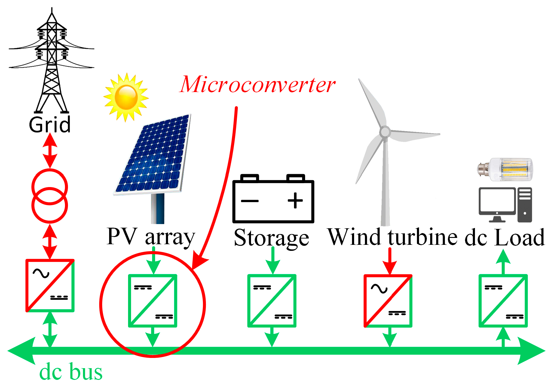
This paper focuses on comparing different inductor designs for high-frequency DC–DC converters that can be used in many applications. The target converter application is a microconverter for a single PV panel (
Figure 1).
2. Definition and Design of Mutual Inductance
As mentioned above, reducing the size of power electronic converters can be achieved by using high-frequency switching. Resonant circuits are employed to enable zero-voltage switching (ZVS) operation of the converter at high frequencies. The well-known LLC converter includes a resonant tank on the primary side of the transformer [
37,
38]. The LLC topology can incorporate either a half-bridge or a full-bridge switch configuration on the primary side [
39,
40,
41].
Table 1 shows the parameters of the prototype, based on which the comparison of mutual inductance will be made.
2.1. Design of the Mutual Inductance
Several design cases considering mutual inductances based on the parameters in
Table 1 are thoroughly analyzed. The main objective is to identify an optimal trade-off between cost, manufacturability, and electromagnetic performance. In this context, both skin and proximity effects will be taken into account to accurately evaluate resistance, inductance value, and associated power losses in different configurations.
To accurately analyze the impact of high-frequency effects on coil performance, electromagnetic simulations will be carried out using ANSYS 2023 R1, a professional software environment for field-based modeling. It will be used to visualize magnetic field distribution, estimate frequency-dependent losses, and evaluate critical parameters such as inductance, coupling coefficient, and resistance across different design cases.
2.1.1. Mutual Inductance Design Based on Litz Wire
The most practical solution for magnetic component design is to use Litz wire, which helps minimize both skin and proximity effects at high frequencies.
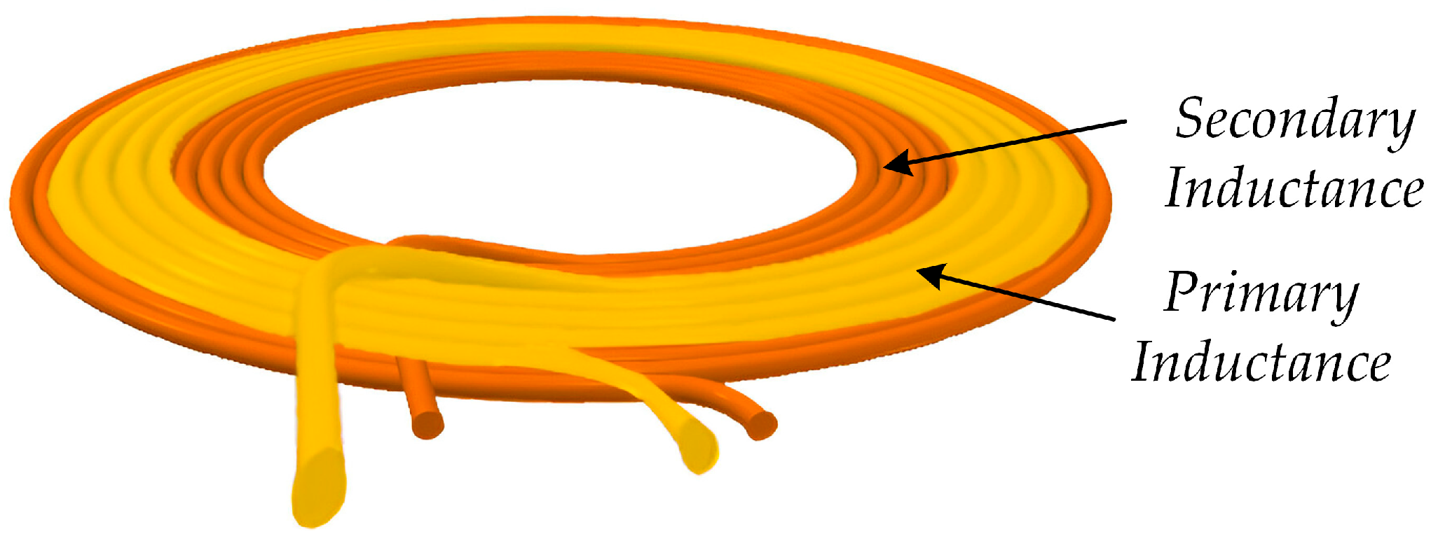
Figure 2 illustrates the concept of a ferrite-less mutual inductance structure based on Litz wire, where the primary winding is shown in yellow and the secondary winding in orange.
To achieve the required inductance values specified in
Table 1, the appropriate number of turns was determined through preliminary calculations and simulations. On the primary side, a total of 3 turns was implemented, while the secondary side consists of approximately 22 turns to meet the inductance target.
In addition, the primary winding is constructed using parallel conductors, which improves the magnetic coupling and enhances the overall coupling coefficient between the windings. This configuration provides a compact and efficient design without the use of magnetic cores, making it suitable for lightweight and cost-effective wireless power transfer applications.
Figure 3a shows the 3D model of the mutual inductance created in ANSYS, which was analyzed to evaluate electromagnetic behavior and field perturbations. The simulation reveals the presence of the skin effect in the current distribution. Although high-frequency Litz wire typically consists of up to 2000–4000 fine insulated strands to suppress both skin and proximity effects, the simulated model was limited to 40 strands due to the computational limitations of the laboratory PC. Since ANSYS does not simulate thermal effects, this resistance increase due to temperature is not captured in the simulation. The ANSYS model focuses only on magnetic behavior, not on thermal phenomena. As a result, the skin effect appears more pronounced in the simulation than in reality.
Nevertheless, even with this reduced strand count,
Figure 3b illustrates that the current density remains relatively uniform across the cross-section of the conductor. Specifically, the current density at the edge of the Litz wire reaches approximately 2.36 × 10
5 A/m
2, while in the center region, it ranges between 3.14 × 10
4 A/m
2 and 6.29 × 10
4 A/m
2. These values show that the current is not concentrated only at the edges but still flows through the inner part of the wires. In practical implementation, where thousands of strands are used, the influence of the skin effect would be reduced. This model still provides a meaningful approximation for analyzing magnetic field distribution and validating the coupling characteristics of the mutual inductance under constrained simulation conditions.
2.1.2. Mutual Inductance Design Based on PCB
Since the operating frequency is relatively high and the theoretical nominal values of the inductances are quite low, the inductors can be implemented directly into the PCB structure. This approach results in a planar, lightweight, and cost-effective design, as single or double-layer PCBs are inexpensive to fabricate.
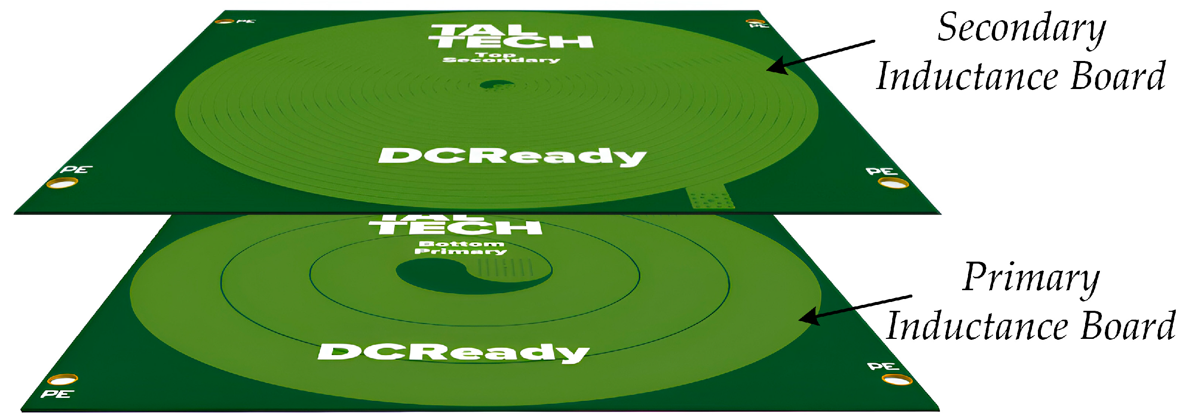
Figure 4 presents the 3D model of the PCB-based mutual inductance concept, designed in Altium Designer. The design consists of two separate two-layer PCBs: one for the primary winding and one for the secondary winding.
The primary inductance includes around three wide tracks to handle higher current and improve coupling, while the secondary inductance comprises more than 20 turns made with narrow tracks, which is sufficient due to the lower current on the secondary side. This configuration allows for compact integration, mechanical stability, and easy assembly without additional magnetic components.
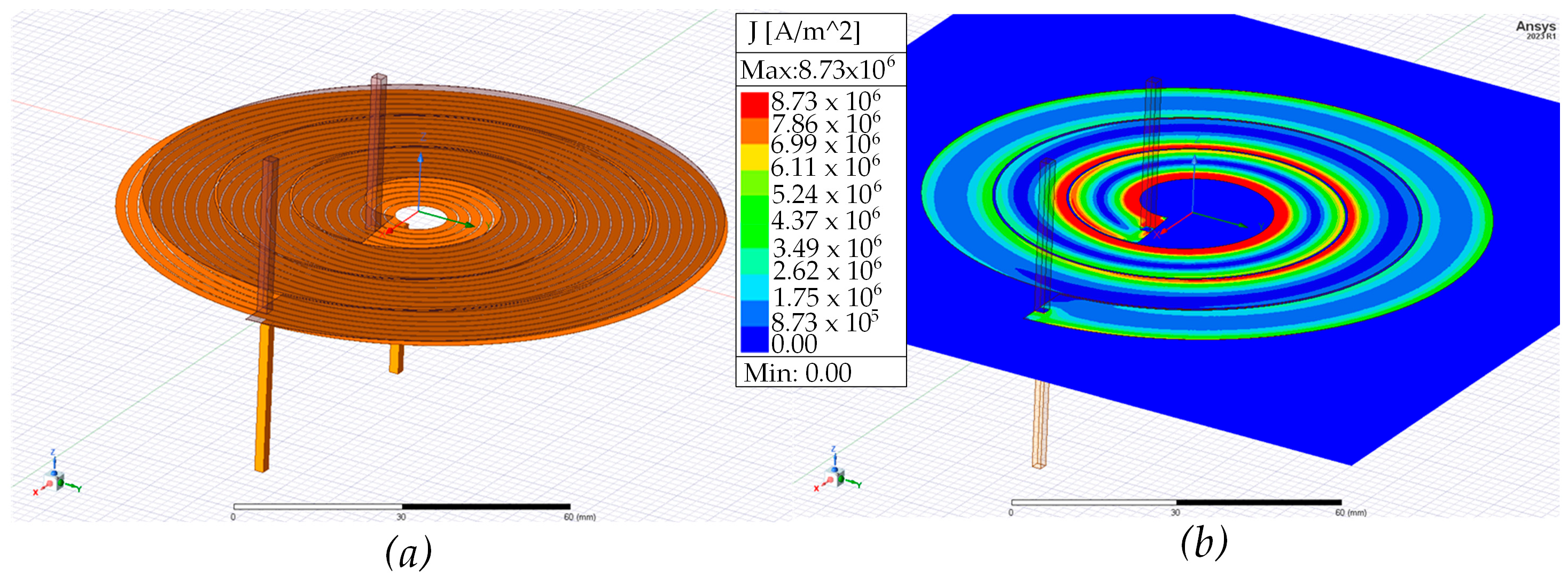
Similarly, this PCB-based approach was simulated using ANSYS software to evaluate the impact of skin and proximity effects at high frequency.
Figure 5a shows the 3D model of the mutual inductance realized on a PCB without any magnetic cores, while
Figure 5b presents the resulting current distribution along the copper tracks. Simulation results indicate that the skin effect is highly pronounced in this configuration. A large portion of the current is concentrated along the edges of the tracks, rather than uniformly distributed across the cross-section.
Additionally, a significant proximity effect is observed. Most of the current is concentrated in the inner turns, near the center of the PCB, while the outer turns carry noticeably less current. The current density near the edges of the tracks reaches approximately 8.73 × 10⁶ A/m2, whereas the current density in the central region is around 8.73 × 10⁵ A/m2. This current distribution leads to increased resistance and, consequently, higher power losses.
2.1.3. Based on Hybrid Design Approach: Litz Wire and PCB
The final case refers to a hybrid approach for designing the mutual inductance. The concept is to implement the primary winding using a PCB-based layout, while the secondary winding is realized with Litz wire, as illustrated in
Figure 6. This configuration aims to achieve a balance between cost, weight, and high-frequency performance, particularly in reducing the impact of the skin effect.
Using a PCB for the primary side allows for compact and low-cost manufacturing, while the Litz wire on the secondary side ensures lower resistance and better efficiency under high-frequency operation. This hybrid solution is especially suitable when moderate current flows through the primary side and higher winding quality is required for the secondary side.
However, the proximity effect is more pronounced in this case, as the majority of the current becomes concentrated near the center of the mutual inductance, where the windings are positioned closely together.
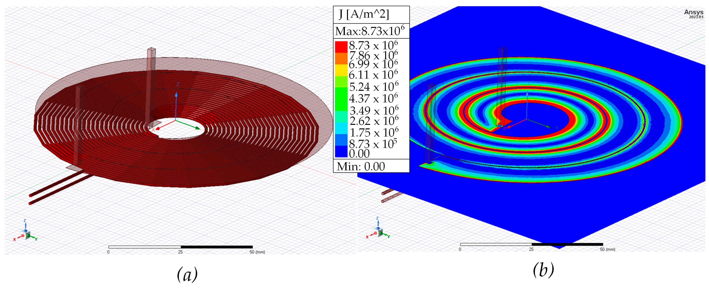
Figure 7a presents the 3D model of the hybrid mutual inductance, while
Figure 7b illustrates the corresponding current density distribution. As observed in the simulation, the current density at the edges of the conductor reaches approximately 8.73 × 10
6 A/m
2, while in the central region it remains around 8.73 × 10
5 A/m
2. This non-uniform distribution confirms the influence of the proximity effect, which contributes to increased resistance.
2.2. Comparison of the Design Approaches
Finally, three mutual inductance design approaches were evaluated and compared in terms of their inductance values and associated resistance under varying current frequencies. It is important to emphasize that the proximity effect is independent of current amplitude, and that the ANSYS simulation environment does not consider thermal effects when calculating resistance. Consequently, the resistance values obtained reflect only the influence of magnetic field interactions and related current distribution phenomena.
The evaluation was conducted at two representative operating conditions, corresponding to different RMS current levels for the primary and secondary sides. The results are presented in
Figure 8, which illustrates the frequency-dependent behavior of the inductance in the range from 100 kHz to 2 MHz.
Figure 8a shows the performance of the primary inductance for all three designs. It can be observed that the PCB-based implementation exhibits a pronounced reduction in inductance with increasing frequency, which is attributed to its susceptibility to proximity effects. In contrast, the Litz-wire-based design demonstrates superior stability, with the inductance remaining relatively constant over the entire frequency range. The hybrid PCB–Litz wire solution lies between these two extremes, exhibiting moderate sensitivity to frequency.
A comparable pattern is observed for the secondary inductance. Although the number of winding turns is approximately the same, the PCB-based design yields a lower inductance value, which may negatively influence the voltage gain. Nevertheless, across the considered frequency range, the nominal inductance values on the secondary side remain largely unaffected. Inductance estimation is crucial at high frequencies, as selecting the appropriate capacitor value is necessary to achieve ZVS.
The most important aspect is the relationship between the inductance resistance and frequency.
Figure 9 illustrates the resistance of the inductors as a function of current frequency, highlighting the impact of skin and proximity effects on different mutual inductance design approaches. Clearly, the Litz-wire-based mutual inductance exhibits low resistance for both the primary (
Figure 9a) and secondary (
Figure 9b) windings, with resistance remaining almost constant as frequency increases. In contrast, the PCB-based and hybrid mutual inductances show significantly higher resistance at elevated frequencies, primarily due to intensified skin and proximity effects in planar conductors.
These dependencies are crucial for understanding the magnetic losses and their influence on overall system efficiency, especially in high-frequency applications. The increased resistance in PCB-based and hybrid designs leads to greater power dissipation and reduced performance, which must be carefully considered during the design phase. Ultimately, this analysis aids in selecting the optimal mutual inductance design by balancing manufacturing cost, physical size, weight, and electrical performance, ensuring reliable operation under the targeted frequency and current conditions.
3. Experimental Prototypes
To validate the proposed concept, all considered mutual inductance designs were physically implemented.
Figure 10 presents the fabricated prototypes of mutual inductances intended for integration with the PV microconverter. The inductance and resistance values were measured using a programmable RLC bridge (Rohde & Schwarz HM8118, Munich, Germany), which allows precise impedance characterization at frequencies up to 200 kHz.
Figure 10a–d presents the PCB-based air core mutual inductance. Each PCB has outer dimensions of 10.5 × 10.5 cm
2, with a copper track thickness of 70 µm. The measured value of the primary inductance is approximately 500 nH, while the secondary inductance is 19.86 µH. These experimental results are in good agreement with the simulation data and confirm the viability of this design for high-frequency power transfer applications.
The measured coupling factor is approximately 0.9, indicating efficient magnetic linkage between the coils. The resistance of the primary winding is 66 mΩ, while the secondary winding has a resistance of 3.1 Ω. These values highlight the increased resistance on the secondary side due to the greater number of turns and thinner track geometry.
Figure 10e,f show the experimental mutual inductance prototype based on the hybrid design, which combines a PCB-based primary winding with a Litz-wire-based secondary winding. The overall dimensions remain identical to the PCB-based version, as the primary inductance is still implemented on a PCB. However, the electrical parameters differ due to the use of Litz wire on the secondary side. The measured primary inductance is 570 nH, and the secondary inductance is 24.9 µH. The coupling factor is approximately 0.85, indicating a slightly lower magnetic coupling compared to the fully PCB-based design. The resistance of the primary winding is 43.9 mΩ, while the secondary resistance is 2.2 Ω. This configuration offers a compromise between reduced skin effect losses and moderate manufacturing complexity.
Finally,
Figure 10g,h present the mutual inductance prototype based entirely on Litz wire. In this case, the measured inductance values closely match those obtained from the ANSYS simulations. The primary inductance is 440 nH, and the secondary inductance is 25.9 µH. The coupling factor is approximately 0.67, indicating strong magnetic coupling. The overall size of the mutual inductance is 8 × 9 cm with an elliptical winding layout. The used Litz wire consists of 3000 strands each with a diameter of 0.05 mm for the primary side coil and 45 strands each with a 0.01 mm diameter for the secondary coil, providing a high surface area to effectively minimize skin and proximity effects at high frequencies. The measured resistance of the primary winding is 7.7 mΩ, and that of the secondary winding is 266 mΩ. It should be noted that all parameters were measured at a test frequency of 200 kHz.
An experimental prototype was developed to validate the theoretical calculations, as shown in
Figure 11a. The converter is based on series–parallel (SP) compensation.
Figure 11b presents the assembled test setup, including the converter and mutual inductance interconnected on the workbench with appropriate probe connections. For the experimental validation, the nominal voltage of the DC grid was set to 350 V. The converter operated with an input voltage of 40 V and delivered an input power of 450 W. Additionally, the converter includes an output relay and an inductive filter.
Several instruments were employed during the experimental evaluation: a Precision Power Analyzer (Yokogawa WT1806E, Tokyo, Japan) was used for efficiency measurements, signal waveforms were captured using a Tektronix MSO4034B (Eindhoven, The Netherlands) oscilloscope with compatible voltage and current probes, current measurements were supported by a Rogowski coil, resistive load, and the DC supply was provided by a TDK Lambda (Düsseldorf, Germany) GEN150-22 programmable source.
The power stage of the converter includes GaN transistors (GS61008PTR) as switches S1–S4. These devices feature a maximum on-state resistance RDSON of 9.5 mΩ and an output capacitance ranging from 200 pF to 300 pF at the operating switching frequency of 1.3 MHz, making them suitable for high-efficiency, high-frequency applications. On the output side, SiC Schottky diodes (C6D10065E) are used as rectifiers, having a breakdown voltage of 650 V and a maximum continuous forward current rating of 10 A.
To validate the concept, a simple open-loop control strategy was implemented. Each PWM channel was operated with a 50% duty cycle, sufficient for evaluating the converter behavior and mutual inductance performance under the defined test conditions.
Figure 12 presents the experimental results of the step-up DC–DC converter utilizing PCB-integrated mutual inductance based on the hybrid design approach. The voltage waveform across the primary-side transistor is shown in
Figure 12b. The waveform indicates ZVS conditions, as the transistor turns off with a non-zero current and the current has a negative phase shift related to the voltage. This confirms that soft switching is achieved, which significantly reduces dynamic losses and enables efficient operation at high switching frequencies. Simultaneously,
Figure 12a,b display the voltage and current waveforms on the secondary side. Based on the waveform, the resonant frequency can be estimated. The resonant half-period is approximately 375 ns. Considering that the primary series capacitor is 123 nF and the coupling factor is 0.85 for the hybrid configuration, the calculated inductance is 417 nH. This value closely matches the result shown by the blue line in
Figure 8a at 1 MHz. This result validates the ANSYS simulation.
The secondary voltage exhibits a truncated sinusoidal shape due to the absence of a filter inductor after the rectifier. Nevertheless, this configuration helps to smooth the voltage across the rectifier diodes and mitigates voltage overshoots during switching transitions.
Figure 12c shows the measured input and output voltages and currents of the converter, demonstrating stable operation under the defined load and switching conditions.
The most critical findings were obtained through thermal analysis of the converter operating with different mutual inductance configurations. Thermal behavior of the mutual inductors, along with GaN transistors, was evaluated under full-load conditions.
Figure 12d–f present the thermal images of the various mutual inductance prototypes captured using a Fluke thermal imaging camera. As expected, the Litz-wire-based mutual inductance demonstrated the best thermal performance, exhibiting minimal losses. In particular,
Figure 12f shows that the surface temperature did not exceed 35 °C during operation. In this configuration, the converter achieved an efficiency of approximately 94%.
In contrast, the PCB-based mutual inductance experienced a substantial temperature rise, reaching up to 175 °C, as shown in
Figure 12d. This significant heating correlates with higher resistance due to pronounced skin and proximity effects. The corresponding converter efficiency dropped below 87%.
The hybrid configuration, combining a PCB-based primary side with a Litz-wire secondary side, provided intermediate results. As illustrated in
Figure 12e, the peak temperature remained below 100 °C, and the measured efficiency was around 91%.
Moreover, as confirmed by the ANSYS electromagnetic simulations, the proximity effect in the PCB-based mutual inductance forces the current to concentrate primarily in the central region of the conductor, leading to increased resistance and localized heating. A similar effect was observed in the hybrid configuration; however, the current distribution was spread over a larger PCB area due to the wider layout of the primary winding. As anticipated, the Litz-wire-based mutual inductance did not exhibit noticeable proximity effects, owing to the fine, individually insulated strands that uniformly distribute the current across the cross-section and significantly reduce both skin and proximity effects at high frequencies.
Experimental and simulation results showed that different designs of mutual inductance lead to different coupling factors. PCBs are inherently flat, which results in minimal alignment deviations in the design. However, Litz wire does not have a rigid structure and is flexible. Therefore, the alignment is not perfectly flat as the PCB and depends on the surface of the planar Litz-wire-based coil. Paper [
42] explains the dependence of mutual inductance on the coil distance and their alignment. As a result, the greater the distance between coils, the lower the coupling factor; similarly, a smaller alignment area also causes a decrease in the coupling factor. At the same time, at lower coupling factors, the high gain range is reduced [
43].
4. Comparison of the Design of Mutual Inductances
Figure 13 presents the power loss distribution of the DC–DC converter, while
Figure 13 illustrates the coil losses for different design approaches over a range of operating frequencies. The results indicate that the primary side coils contribute significantly to the overall losses, particularly in the hybrid and PCB-based implementations. Although the secondary side inductors exhibit comparatively lower losses, both the hybrid and PCB approaches still result in higher losses than the Litz wire configuration. Since the converter was tested at an operating frequency of approximately 1 MHz, the power loss distribution shown corresponds to this specific condition. Auxiliary losses, which include power consumption by the control and measurement systems, amount to 2 W.
Semiconductor losses consist of conduction losses in the primary-side GaN transistors (four switches), secondary-side SiC rectifier diodes (four diodes), and the output solid-state relay (SSR), which comprises two Si-based switches connected in series. The on-state resistance of each GaN switch is 9.5 mΩ at room temperature and increases by a factor of 1.45 at a case temperature of 75 °C, according to the manufacturer’s datasheet. The forward voltage drop of each SiC diode is 1.8 V. The secondary-side RMS current is proportional to the output current and is calculated as , while the RMS current through the primary-side inductors is proportional to the average input current of 11.66 A, with a proportionality factor of . The total power loss of conduction loss of semiconductors for each design approach is approximately 7.29 W. Inductor losses include conduction losses in both the primary and secondary windings, as well as in the output filter. The resistance of the output filter is 0.1 Ω, and the on-state resistance of the SSR is 280 mΩ. The total inductor loss is calculated to be 3.08 W for the Litz wire approach, 14.09 W for the hybrid approach, and 20.88 W for the PCB-based approach. The remaining losses are attributed to dynamic switching losses in the semiconductors, conduction losses in the PCB traces of the converter, and thermally induced resistive losses in the inductors.
Finally, a cost comparison was conducted for the considered mutual inductance design approaches. The PCB-based design uses a two-layer board with 2 oz copper to reduce resistance and losses. PCB costs are easy to estimate due to the wide availability of manufacturing services. The cost of a single PCB unit is approximately USD 25, which includes both materials and manufacturing. Therefore, the cost of one mutual inductance unit based on PCBs is around USD 50.
However, in the case of mass production, the economics become much more favorable. For example, at a quantity of 100 units, the cost per PCB increases to approximately USD 111, resulting in a total cost of USD 222 per mutual inductance unit for a batch of 100 units.
In the case of Litz wire, the situation is more complex due to limited market availability. Typically, suppliers provide pricing only upon request, and it is also challenging to find companies capable of manufacturing planar inductors using Litz wire. For an honest cost comparison, the specific Litz wire used in the experiments must be considered. The cost of 1 m of 0.05 mm × 3000 strand Litz wire is approximately USD 10.35. For the secondary side, the Litz wire used is 0.1 mm × 45 strands, with a cost of around USD 7 per meter. The estimated manufacturing cost for one unit of planar inductor can be preliminarily set at USD 5. However, in the case of a planar Litz wire inductor, the total length of wire required must be calculated to determine the final cost accurately:
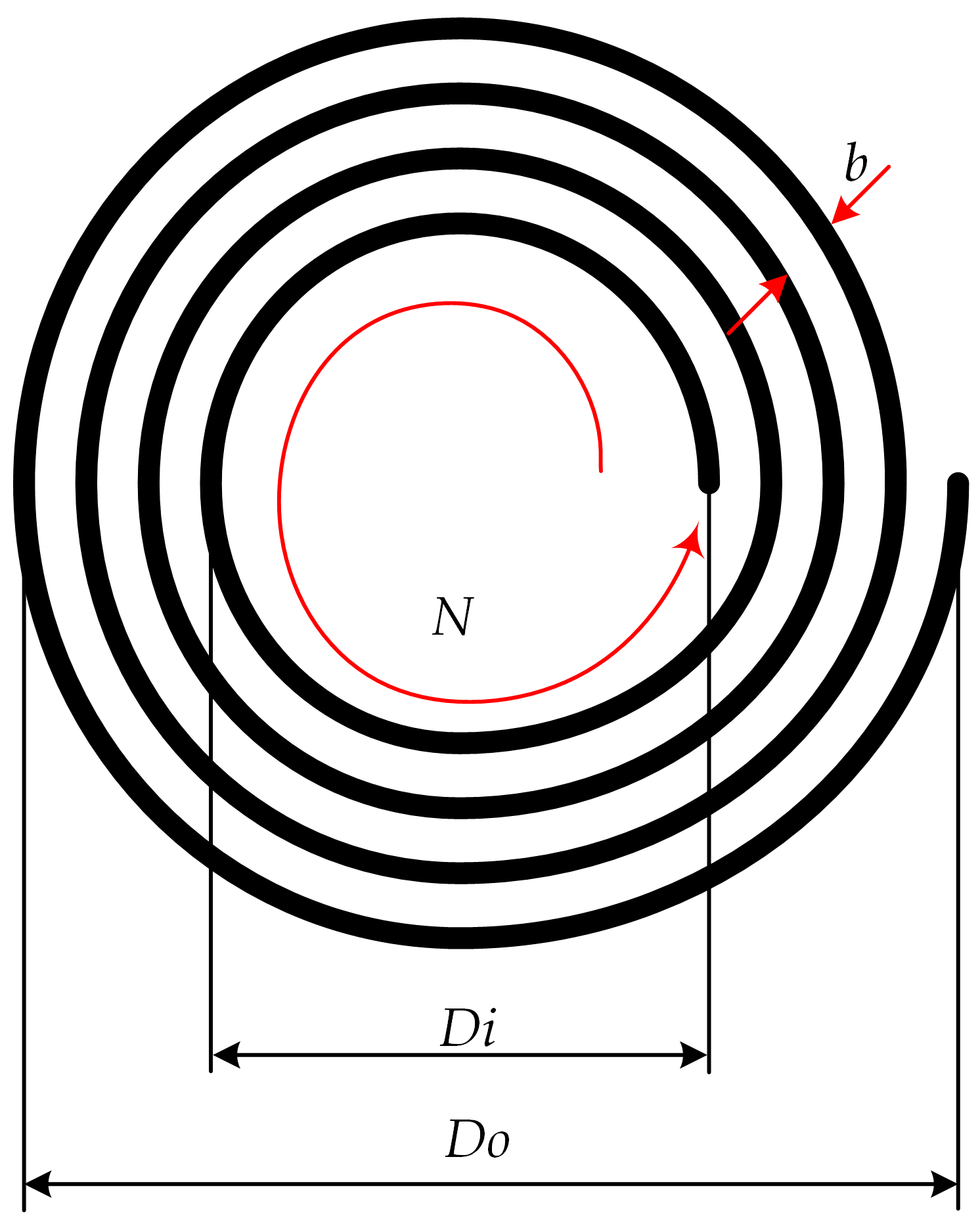
where
Do is outer diameter,
Di is inner diameter, and
N is number of windings.
The inner diameter (
Di in
Figure 14) of the primary-side inductor is 1.9 cm, and the outer diameter is 9 cm, with a total of 3.5 turns. For the secondary-side inductor, the inner diameter is 2 cm, the outer diameter is 7.5 cm, and the number of turns is 23. Based on these parameters and the approximate length calculation method, the total wire length is estimated to be 60 cm for the primary side and 3.43 m for the secondary side. Accordingly, the cost of the primary-side inductor is approximately USD 17.40 per unit, while the cost of the secondary-side inductor is about USD 29.
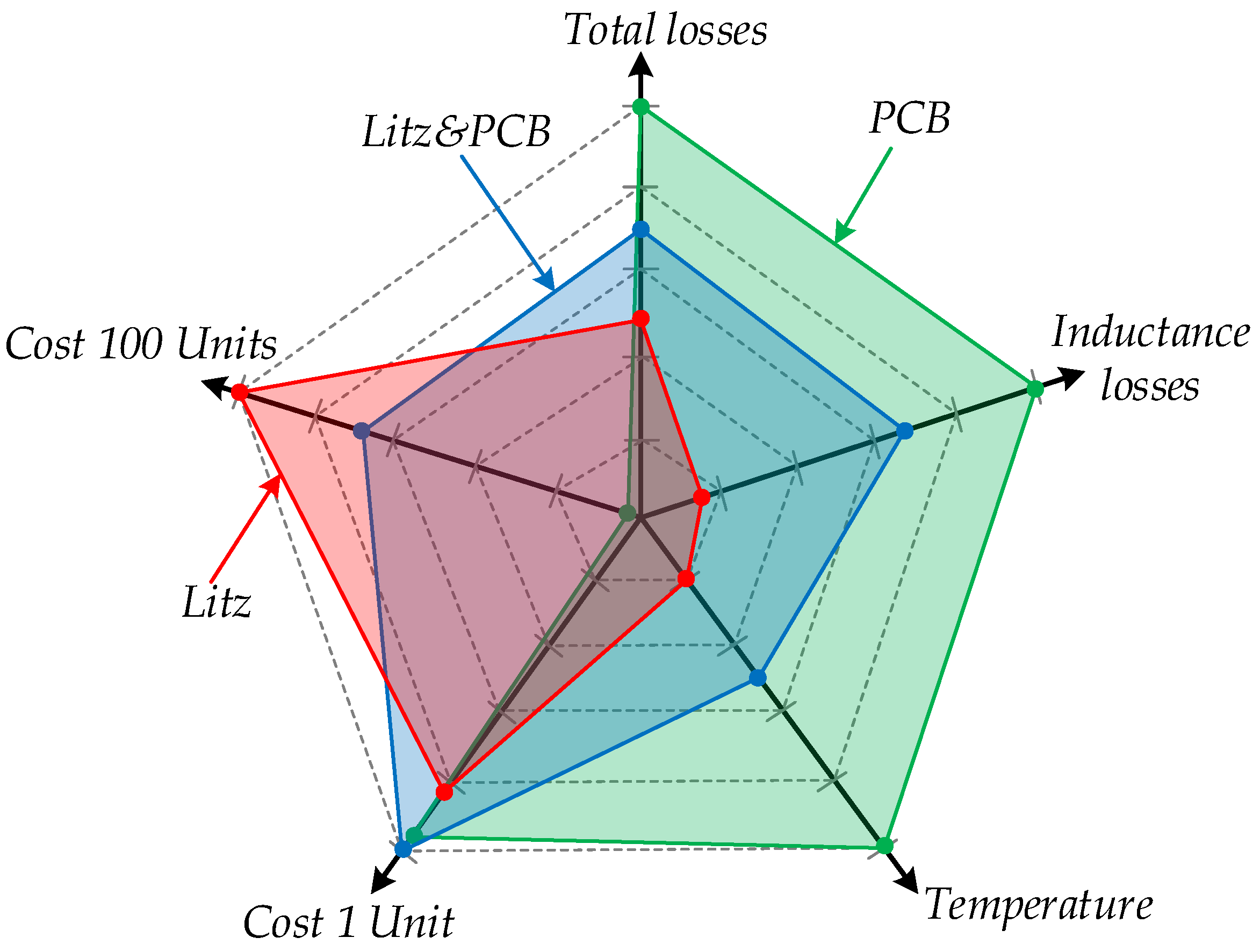
Figure 15 presents the normalized Gantt diagram, which considers several key factors: inductance losses, total losses, inductor temperature, cost per unit, and cost for 100 units. In this diagram, a smaller area corresponds to better overall performance. It can be observed that the PCB-based design (green area) has the largest overall area, indicating lower performance across most parameters. The only parameter where it performs best is the cost for 100 units. Additionally, the cost per unit is nearly the same across all approaches. The hybrid design approach shows balanced performance across all parameters, with its area concentrated around the center of the diagram. The Litz-wire-based design exhibits the lowest power losses but also the highest cost for 100 units. In summary, the Litz wire approach is the most efficient but also the most expensive, while the hybrid design represents a trade-off between all considered parameters and could be viewed as an optimal solution.
5. Conclusions
This paper presented several design approaches for high-frequency air core mutual inductance, focusing on three configurations: Litz-wire-based, PCB-based, and hybrid (Litz wire and PCB). Simulations were performed using ANSYS software, taking into account skin and proximity effects.
The results showed that the PCB-based mutual inductance is highly sensitive to the proximity effect, with the current concentrated at the center of the windings. The hybrid configuration showed a similar pattern, but with a broader current distribution. In contrast, the Litz-wire-based design effectively suppressed proximity effects, resulting in a more uniform current distribution. Consequently, the resistance of the PCB-based design increased significantly at high frequencies, exceeding 5 Ω, compared to 2.5 Ω for the hybrid and just over 1 Ω for the Litz-wire-based design. The primary windings showed similar trends. In terms of inductance, only the Litz-wire-based configuration maintained relatively stable values across the frequency range, while others exhibited decreasing inductance at higher frequencies.
Experimental validation was carried out using a DC–DC converter prototype for PV applications. All three mutual inductance configurations were tested. The experimental results closely matched the simulations. The PCB-based mutual inductance showed the lowest efficiency (below 87%) and a concentrated current path. The hybrid design achieved an efficiency of over 91%, while the Litz-wire-based mutual inductance demonstrated the highest efficiency at 94%. In all cases, the temperature of the mutual inductance remained below 35 °C. Experimental waveforms confirmed ZVS operation. The main drawback of the Litz-wire-based design is its lower coupling factor, caused by reduced coil contact area due to its construction. The findings of this study can support the further development of compact, lightweight, and cost-effective converters for PV applications, along with further PCB-based inductor optimization to minimize proximity effect.
