Article

An Overview of Analog and Digital RF Generator Techniques, Suitable for Space-Based AOTF Applications

by
Jurgen Vanhamel
1,2
1
Faculty of Aerospace Engineering, TU Delft, Kluyverweg 1, 2629 HS Delft, The Netherlands
2
Electronic Circuits and Systems, KU Leuven, Kleinhoefstraat 4, 2440 Geel, Belgium
Appl. Sci. 2025, 15(15), 8739; https://doi.org/10.3390/app15158739
Submission received: 6 June 2025 / Revised: 18 July 2025 / Accepted: 19 July 2025 / Published: 7 August 2025
(This article belongs to the Special Issue Recent Advances in Space Instruments and Sensing Technology)

Abstract

The use of Acousto-Optical Tunable Filters (AOTFs) is well known in ground- and space-based applications. These devices are used in several optical instruments and payloads for monitoring and other purposes. To make use of the filter capability of the AOTF, a dedicated Radio Frequency (RF) chain, consisting of an RF generator and RF amplifier, is needed. An RF generator can be designed in several ways. However, the design of these steering devices for space applications comes with several difficulties and limitations. The mechanical stress due to shock and vibration, the temperature variation, as well as the vacuum environment and radiation levels in which these devices have to perform limits the selection of possible techniques. This paper aims at giving an in-depth overview of space-qualified RF generator techniques using Commercial-Off-The-Shelf available components that usable in the harsh environment of space and applicable in driving AOTFs. Several analog as well as digital generator principles are discussed, substantiated by test results.

1. Introduction

Acousto-Optical Tunable Filters (AOTFs) are used in many different ground- and space-based applications for different purposes [1,2,3,4,5,6,7]. The device can act as a filter in order to select optical wavelengths of interests at a high spatial and temporal resolution [4,8,9,10,11].
The working principle of an AOTF is based on the interaction between soundwaves and light, having birefringence and consequently creating the filter capability. This sound–light interaction occurs in an area called the acoustic column (Figure 1). Due to the photo-elastic effect, the refractive index of the AOTF is changed. The velocity of these soundwaves, propagating through the AOTF, depends on the used material of the crystal [12,13]. The soundwaves inside the AOTF are generated using an RF signal, which is applied to a transducer, mounted at the side of the crystal (Figure 1). The transducer, which includes a piezoelectric layer, is able to convert this RF signal into acoustic waves that propagate inside the AOTF’s crystal. In order to convert the applied RF power efficiently, the transducer needs to be matched in two ways. On the one hand, the mechanical matching has to be carried out on the optical crystal, but on the other hand the electrical matching should fit on the RF side. In order to activate the filter capability of the AOTF in an efficient way, the pure sinewave RF signal has to have a specific frequency and power level. This RF signal is generated by an RF chain, consisting of an RF generator and RF amplifier (Figure 1). The RF generator generates a single-frequency RF carrier, having a certain amplitude. The level of this signal is additionally increased in amplitude by the RF amplifier.
The generation of the RF carrier can be achieved in several ways. Nevertheless, if the RF chain-AOTF setup is used for space-based applications, the design is prone to several limitations. The latter are related to the space environment in which these devices have to function. In order for the setup to survive in space, a wide variety of environmental tests is carried out prior to launch: I.c. thermal-vacuum tests, shock, vibration, radiation, and EMC/EMI tests. Hence, the selected RF generation designs have to be in-line with this approach. The selection of components needs to take into account the limitations listed above and additionally, and the design has to be aligned with the ECSS (European Cooperation for Space Standardization) standard of ESA and comparable rules imposed by other agencies. Consequently, existing RF designs applicable in commercial applications are not one-to-one transferable into a space-grade design. This severely limits the feasibility of RF generator techniques to those who can fulfill these specific requirements and rules.
In this paper, five space-grade RF generator techniques, based on Commercial-Off-The-Shelf (COTS) components, are addressed, both digital and analog in origin. The approach is carried out in such a way that the design uses COTS components that have an exact comparable space-grade counterpart available. Hence, each technique is one-to-one convertible into a space-grade model, having the same performance as the COTS based version. All of the proposed techniques are discussed, additionally supported by analysis and, if possible, physical tests.

2. AOTF Working Principle

Depending on the applied power level and frequency, a different optical wavelength is refracted at the output of the AOTF. Having a linear polarized light beam at the entrance, the birefringence causes two light beams to exit the AOTF at a specific angle (Figure 1). The diffracted and undiffracted light beams are created if the applied light beam is at the specific Bragg angle θB [15]. Only those wavelengths of interests (diffracted beam under θD) can be used for analytic purposes (e.g., imaging). The other beam under θB is optically blocked.
The intensity of the output depends on the material of the crystal and on the Diffraction Efficiency (DE) of the AOTF. The latter can be approximated by
D E   s i n 2 π 2   M 2     L   P A 2   H   λ 2 ,
in which L and H are the dimensions of the transducer, λ the optical wavelength, PA the acoustic power inside the crystal, and M2 the figure of merit [16]. The latter can be calculated as
M 2 = n i 3   n d 3   p 2 ρ   v 3 ,
in which ni and nd are the refractive indices of the incidence and diffracted light beam, respectively; v is the velocity of the acoustic wave; p is the photo-elastic coefficient; and ρ is the mass density of the material of the crystal.
In order to increase the DE, an optimal RF power needs to be applied to the transducer [12].
P o p t   λ 2   H 2   L   M 2
For the selection of a specific optical wavelength, a dedicated frequency has to be applied to the transducer. This frequency depends on v, λ, θB, the difference ∆n between the diffraction indices, and the angular direction η of the acoustic propagation [17].
f n   v   s i n 2 ( θ B + η ) λ   s i n θ B
Specifically for space applications, the crystal material is typically Tellurium-Dioxide (TeO2), Potassium Dihydrogen Phosphate (KDP), Mercurous Bromide (Hg2Br2), or quartz [18,19,20]. Depending on the used material of the crystal, and the selected optical wavelength domains (e.g., Visible (VIS), Near-Infrared (NIR), or Ultra-Violet (UV)), the applied frequency ranges can vary between 45 MHz and 250 MHz [12].

3. RF Generator Requirements

Several requirements are imposed on the RF generator, all related to the optical wavelength domain and the used AOTF. In Table 1, an overview is given of the driving parameters in the design of an RF generator setup from a general point-of-view. Additionally, in Table 2 specific requirements are listed related to the selected optical domain A distinction has been made between general requirements, which apply to all optical ranges (VIS, NIR, and UV) and specific requirements related to certain optical domains.
This list of requirements flows down from scientific requirements in the frame of ground- and space-based imaging and polarization instruments in which AOTFs are used [3,4,8,21,22,23,24].
The two key parameters that drive AOTFs are the applied frequency and power level. E.g., the driving of a Tellurium-Dioxide (TeO2) AOTF in the VIS and NIR range is achieved by applying an RF power of approximately 300 mW and a frequency between 45 and 120 MHz, while a potassium–dihydrogen–phosphate (KDP) AOTF active in the UV needs around 3 W of power in the frequency range 125 to 250 MHz [12].
These requirements serve as the baseline approach against which the RF generation techniques, listed in the next paragraph, are designed and tested.

4. Space-Qualified RF Generator Techniques

Several RF generator techniques can be used in order fulfil the requirements listed in Table 1. Five different techniques are described, each able to work in the harsh environment of space and using Commercial-Off-The-Shelf components (Table 3). The components used in these generator setups have to withstand tests such as radiation, vibration, shock, thermal cycling, and vacuum. Commercial electronics are not capable of surviving these tests. Hence, the selected components linked to the RF generator techniques are all available in a space-grade package or have a space-qualified version.
The different solutions can be analog or digital, each with their own pros and cons. These five techniques are listed and tested in the following paragraphs. For each technique, the design is described, test results are discussed, and a conclusion is drawn in the frame of implementability for space applications.

4.1. Integrated PLL Design

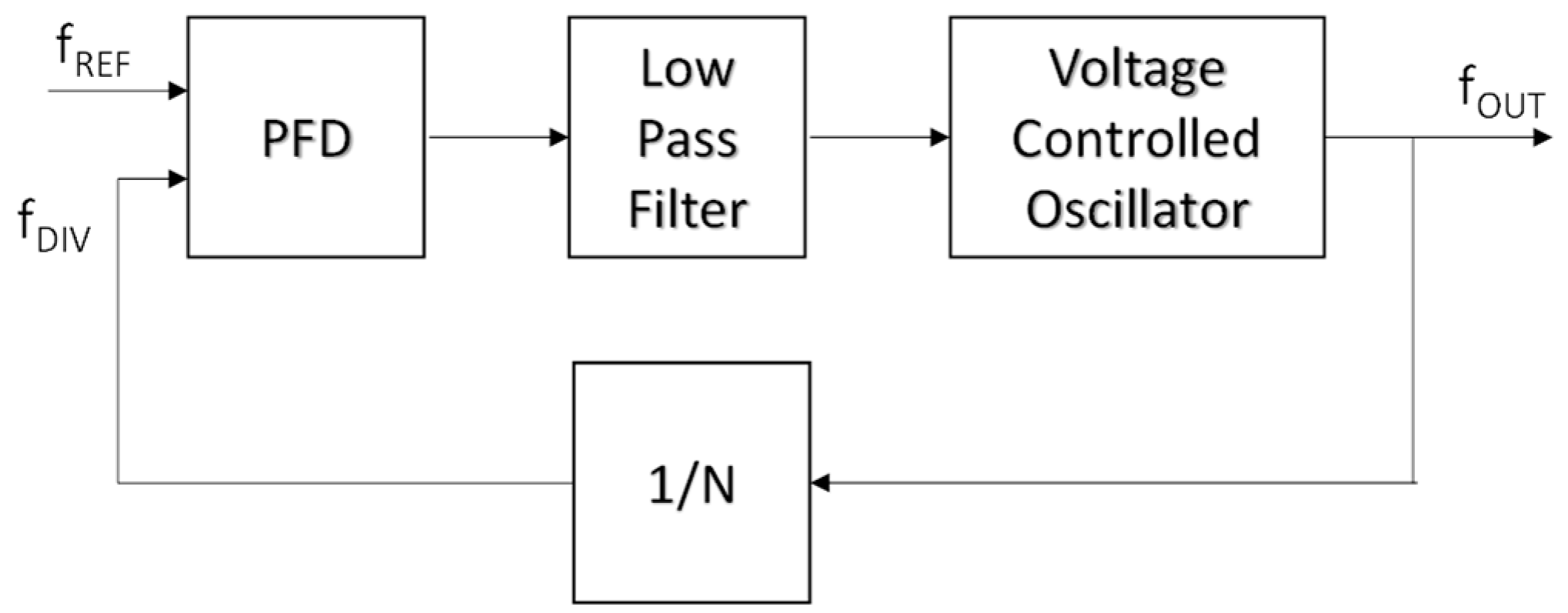
The RF generator in which a Phase-Locked-Loop (PLL) design is used, which already has space heritage [21,25,26]. The top-level topology of the PLL design in shown in Figure 2. The design uses a reference oscillator (fREF), generating a stable reference signal against which the feedback signal (fDIV) is compared in the Phase-Frequency Detector (PFD). If both signals are out of phase, an error signal is generated by the PFD aligned to the phase difference. This signal is converted by a Low-Pass Filter (LPF) into a voltage level capable of driving the Voltage-Controlled Oscillator (VCO) towards the requested frequency. The latter generates the RF output but also feeds back a divided signal (1/N) to the PFD for comparison.
In order to translate this design into a space-qualified setup, the selection of the components has to be carried out in a rigorous way. In Figure 3, the LMX2694 of Texas Instrument (Dallas, Texas, USA) [27] is used as the core of the PLL design. This device has limited space heritage but offers many features. The PLL setup is a fractional N-PLL, using a delta-sigma modulator. The chip houses all the key blocks mentioned in Figure 2. The LMX2694 only needs a reference oscillator of 100 MHz and a 3.3 V power supply, which is common in space designs. The output signal needs additional filtering in order to fulfil the unwanted spectral component suppression requirement of <−30 dBc. The LMX2694 uses several internal VCOs, which create the possibility to generate a wide variety of frequencies at the output (fOUT). The internal VCOs operate between 8.1 GHz and 14.7 GHz. By using internal dividers, the frequency is downscaled to a value between 39.3 and 15,100 MHz, which includes the frequency domain 45–250 MHz, applicable for the VIS, NIR, and UV optical range.
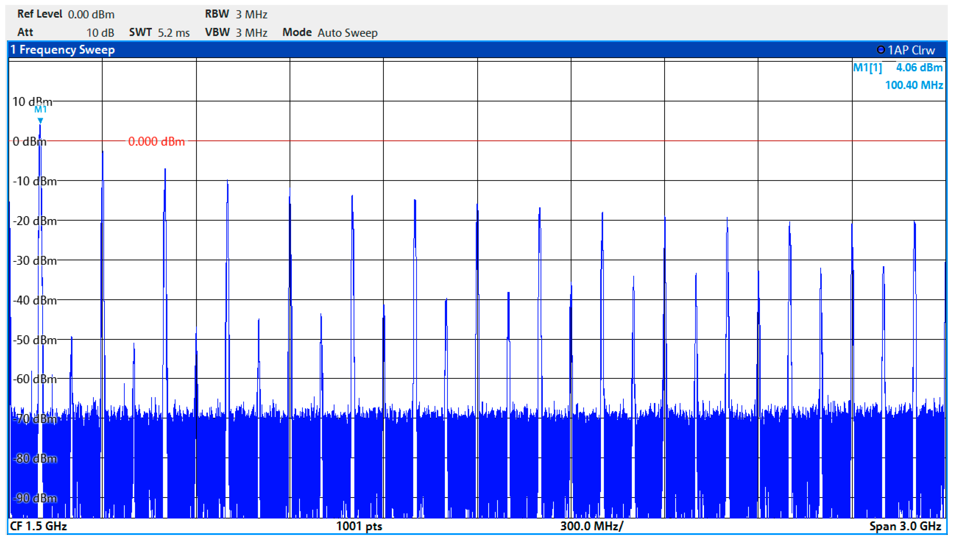
The chip ‘as is’ generates harmonics at the output pin, which need further filtering. As an example, the output spectrum of a 100 MHz signal is shown in Figure 4. The results show that especially the third harmonic level needs additional attenuation. The necessary filter design for a third harmonic suppression is less complex than for a second harmonic suppression. Tests also show that the resolution of the device is 1 Hz, which is much more accurate than requested. The output power level of the chip can be varied by changing the output power setting of the chip. The latter can be programmed, using the external microcontroller (Figure 3). The output power level variates depending on the selected frequency.
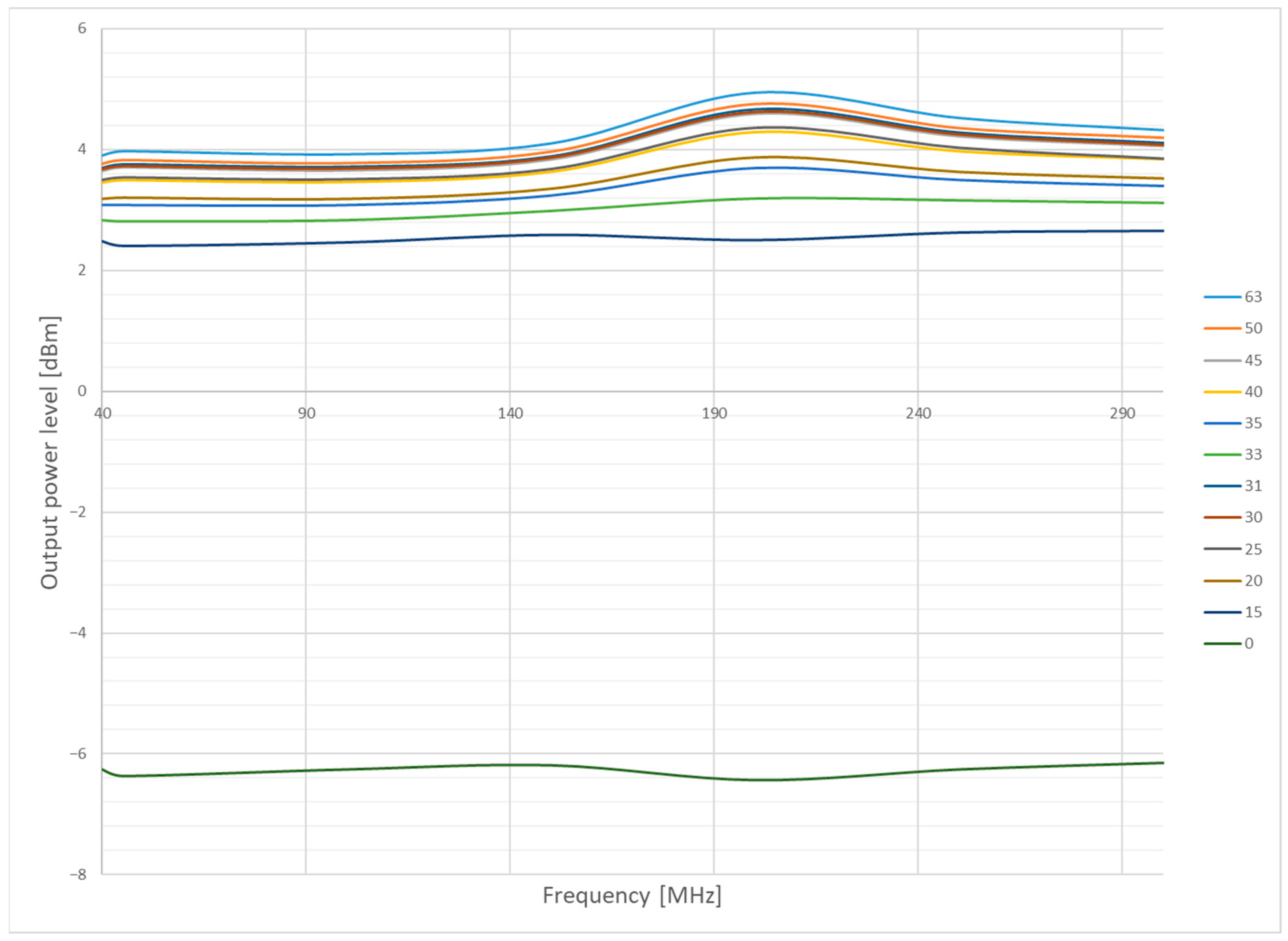
In Figure 5, the frequency is varied between 40 and 300 MHz. The internal current setting, which stipulates the output power, can be set at a value between 63 and 0. The results show a variable output power level between −6 dBm and +5 dBm for the first harmonic. The output power uncertainty is less than 0.01 mW. The power consumption of the chip is around 1 W. The accuracy between 40 and 350 MHz variates between 32 and 115 Hz. The frequency stability is better than 1 Hz, and the stabilization time is less than 5 ms.

4.2. DDS Inside an FPGA

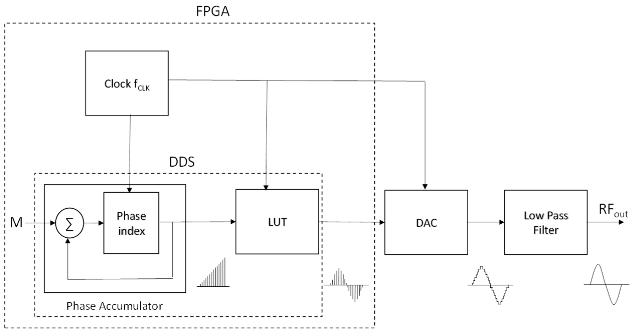
The use of a Direct Digital Synthesis (DDS) RF generator is already established due to multiple space missions [28,29,30]. The principle consists of a of DDS core implemented inside a space-qualified Field Programmable Gate Array (FPGA). The core is written in a hardware description language like Verilog or VHDL. The output frequency RFOUT depends on the tuning word M and on the N-bits wide phase accumulator (Figure 6). By adapting the value of M, the RF output frequency can be changed [31,32]:
R F O U T = M   ·     f C L K 2 N
in which fCLK is the system clock frequency. The output of the phase accumulator is applied to the Lock-Up Table (LUT), in which the phase information is converted into a digital sine wave. The output of the LUT is applied to a Digital-to-Analog Convertor (DAC), which generates a differential output signal. Based on the Nyquist theorem, a minimum of two digital sinewave period samples need to be sent to the DAC for appropriate analog sinewave reconstruction. Practically, the RF output frequency is limited to 30–40% of fCLK [31,32].
The generated output spectrum of the DDS technique is a sampled stepping waveform, having an output amplitude (AmplOUT) with a sin(x)/x dependency. The latter is calculated as [31,32]:
A m p l O U T = s i n π   ·   R F O U T f C L K π   ·   R F O U T f C L K
The spectrum consists of many different harmonics and spurs, which need to be removed in order to generate a pure sinewave. The combination of a balun and a low-pass filter at the output fulfills this task.
Components applicable to be used in space applications, based on the abovementioned technique, are the rad-tolerant DAC5675A-SP of Texas Instruments (Dallas, Texas, USA) [33], combined with a space-qualified Virtex 4 or Virtex 5 FPGA of Xilinx [34]. Taking into account size and power consumption, the Virtex 4 is the preferred choice. This device, having a clock frequency of 400 MHz, is capable of covering the VIS and NIR optical ranges. For the UV range, a frequency doubler is needed. This will impose additional harmonics and spurs that need to be filtered in an adequate manner. As an alternative, the RTAX of the Microchip can be used [35]. A huge disadvantage is the low clock frequency at which this device runs (127 MHz). This will limit the output frequency of the DDS to 50 MHz. This can be circumvented by using a pipelined DDS setup. However, this could possibly cover the frequency range up to the VIS range but certainly not for the UV. A third possible candidate is the RTG4 of the Microchip [36]. This device is able to generate a clock frequency of 400 MHz (comparable with the Virtex 4) but consumes more power, PCB area, and mass. A fourth option is the NG Medium FPGA developed by NanoXplore (Sèvres; France) [37]. This device is also able to cover the frequency up to the VIS range.
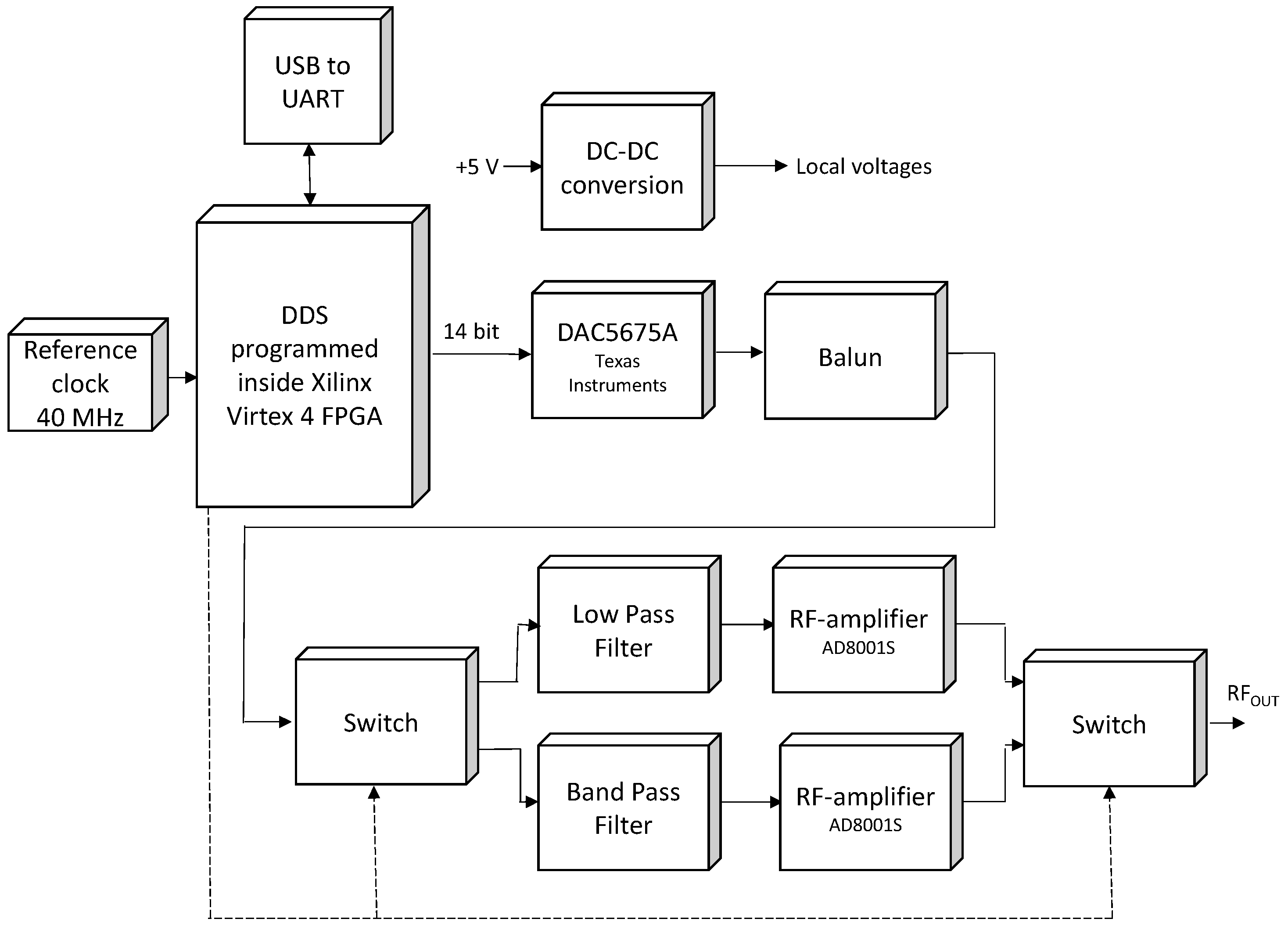
Based on the availability, mass, power consumption, and used PCB area, the Virtex 4 FPGA, combined with the Texas Instruments 14-bit DAC5675A-SP, was used in a test setup (Figure 7). Due to the limited clock frequency of 400 MHz, the VIS optical range (and partially the UV range) can be covered by using a steerable double switch at the output of the setup. This switch is necessary to cover a frequency range of more than one octave (45 up to 180 MHz). Two seventh-order passive Cauer filters (a low-pass filter with a cut off at 90 MHz, and a bandpass filter 90–180 MHz) were used, in combination with an AD8001S RF amplifier of Analog Devices [38]. The latter is used to increase to output power level up to an acceptable level (>0 dBm). In order to communicate with the Virtex 4 FPGA, a Universal Serial Bus to Universal Asynchronous Receiver-Transmitter (USB-to-UART) transformer is used. All necessary supply voltages are generated based on a +5 V input.
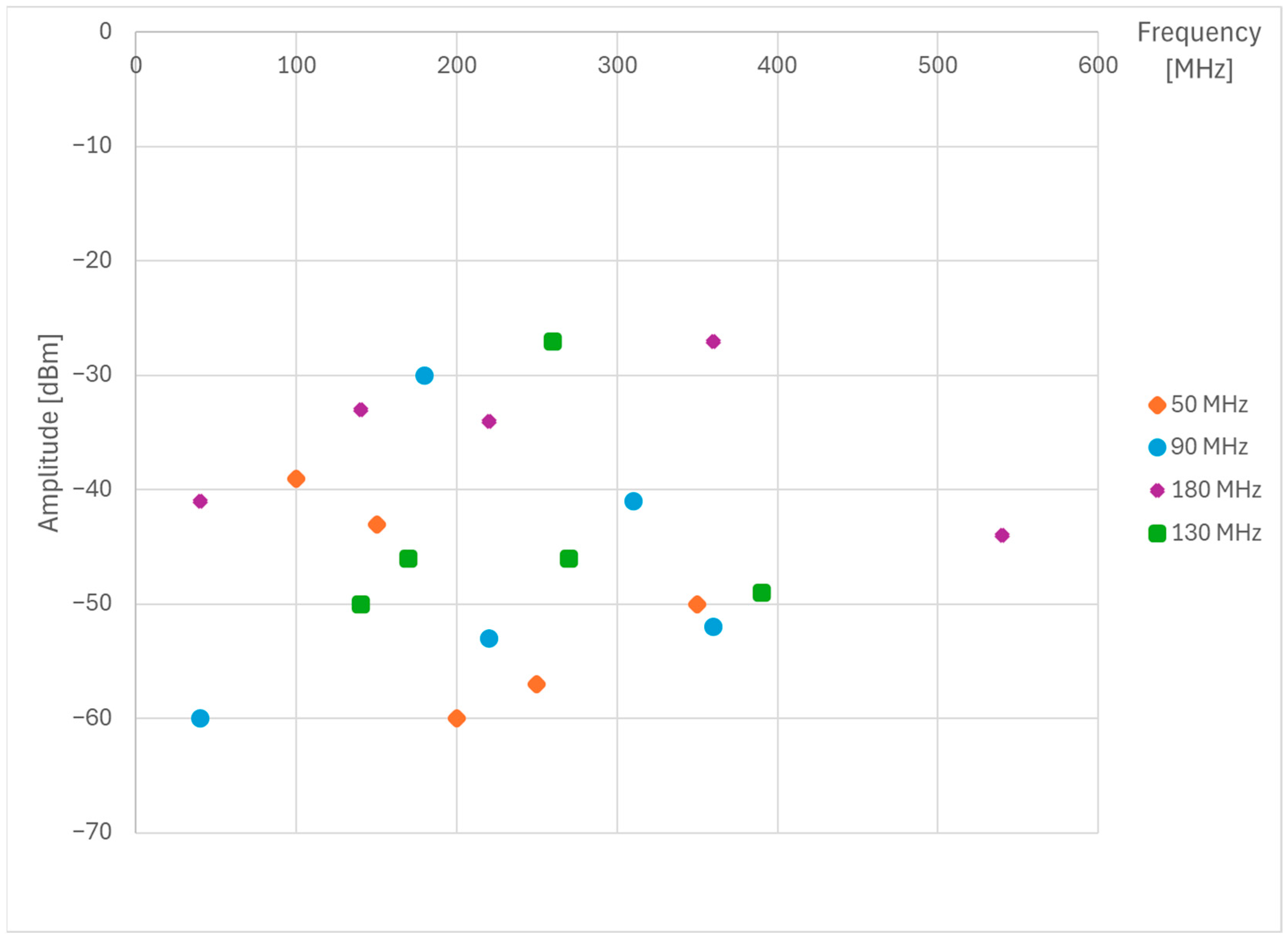
The results show an output power level between +0.5 dBm at 180 MHz and +7 dBm at 45 MHz, depending on the output frequency. The generated harmonics and spur levels are shown in Figure 8 for different generated frequencies. As can be seen, many different spurs and harmonics exist, depending on the selected fundamental frequency. The intensity varies as a function of frequency selection. The power consumption of the setup is 4.1 W for the complete frequency range. This is mainly due to the FPGA-DAC combination. The output power uncertainty is less than 1 mW. Although not necessary for the AOTF application, this setup has the advantage of having a high resolution and accuracy (up to the Hz-range). Also, the requirements of long-term stability and stabilization time are easily met.

4.3. SSB Mixing

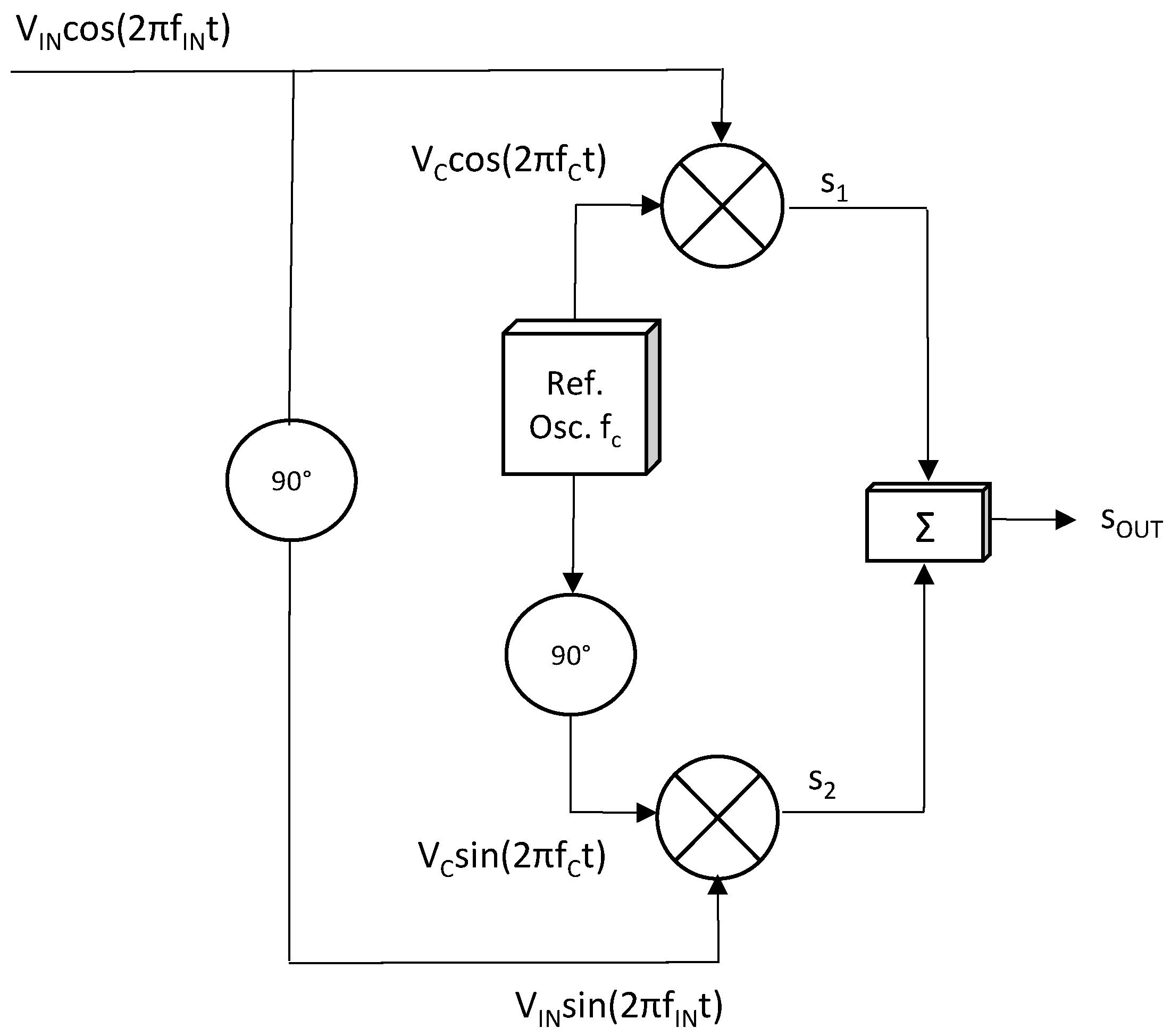
Another more unconventional technique is the use of the Single Side Band (SSB) approach. This mixing principle is a proven technique [39,40,41] and can also be used in the frame of space applications [42]. In this approach, a reference oscillator signal fc is used, shifted by 90° and applied to two separate mixing devices (Figure 9).
The incoming signal [VINcos(2πfINt)], in which VIN represents the amplitude of the input voltage and fIN the frequency of the input signal, is also shifted by 90° and applied to the two mixing devices. Both outputs (s1 and s2) are summed, which creates the requested RF output signal sOUT.
The signal in the upper chain can be written as
s 1 = V I N ·   V C · cos 2 π f I N t ·   c o s ( 2 π f C t )
in which VC is the amplitude of the oscillator signal and fC the frequency of the oscillator. For the lower chain, the following signal is formed:
s 2 = V I N ·   V C · sin 2 π f I N t ·   s i n ( 2 π f C t )
Rewriting these formulas generates
s 1 = V I N · V C   2 · cos 2 π ( f C + f I N ) t + cos 2 π ( f C f I N ) t
s 2 = V I N · V C   2 · cos 2 π ( f C f I N ) t cos 2 π ( f C + f I N ) t
Adding up or subtracting both signals generates the RF output signal sOUT:
s O U T = V I N · V C   ·   cos 2 π ( f C f I N ) t ,
or
s O U T = V I N · V C   ·   cos 2 π ( f C + f I N ) t
Equation (9) is known as the Lower Side Band (LSB) signal, and Equation (10) as the Upper Side Band (USB) signal. Hence, the output frequency can be generated from fCfIN (for the LSB setting) up to fC + fIN (for USB setting).
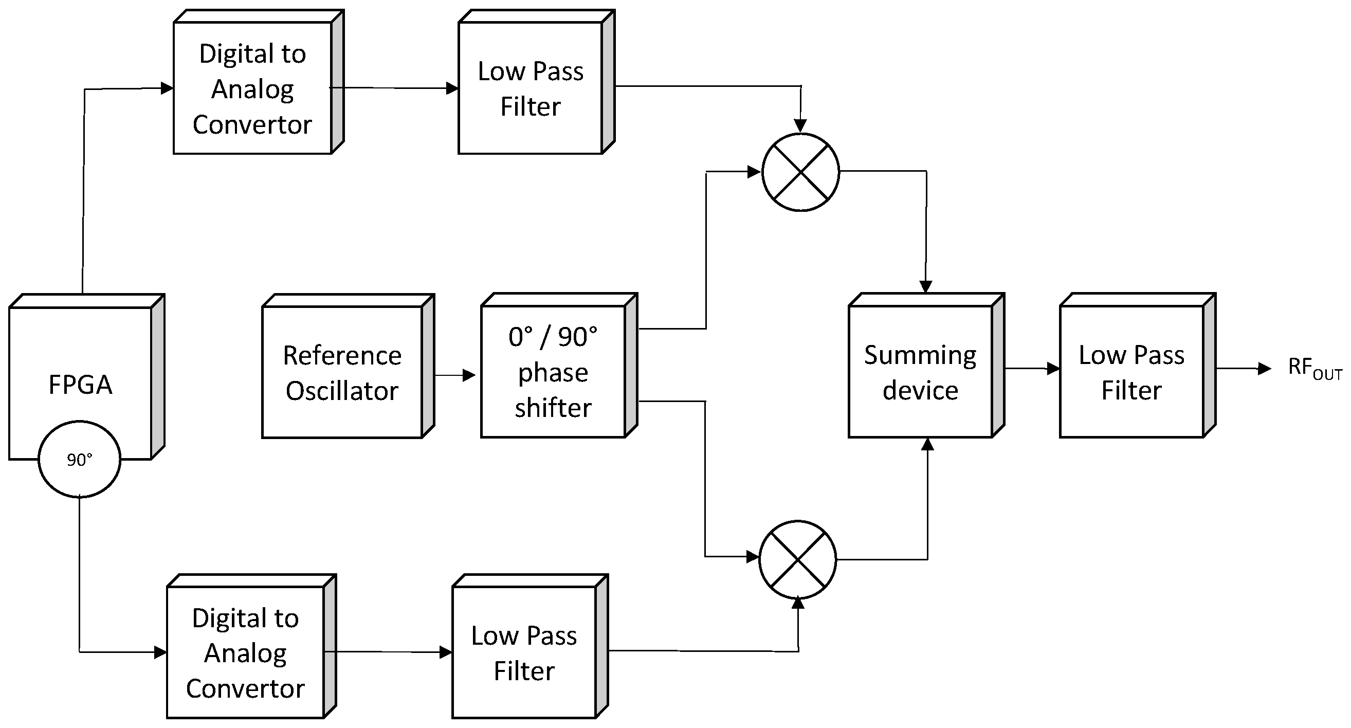
Based on this technique, a bread frequency range can be covered. An example of a space implementable SSB design for the VIS range is shown in Figure 10. The fIN signal can be generated using a DDS inside an FPGA. This approach is explained in paragraph B. The selected space-qualified FPGA can be an RTAX, which runs at a frequency of 127 MHz. Hence, an output signal can be generated after the DAC of 50 MHz, taking the theorem of Nyquist into account [31,32]. The reference oscillator runs at a higher frequency compared to the RTAX-DAC combination.
For each optical wavelength domain (VIS, NIR, and UV), a dedicated reference oscillator and RTAX-DAC combination is needed. E.g., for the VIS range (Figure 7), the RTAX-DAC runs at 30 MHz with a reference oscillator at 90 MHz. Hence, a frequency range generated at the output falls between 60 MHz (=90 MHz − 30 MHz, applying the LSB setting) and 120 MHz (=90 MHz + 30 MHz, applying the USB setting).
The different building blocks in Figure 10 are all available as space-qualified components.
A clear disadvantage of this approach is the amount of building blocks. Hence, the used mass, volume, and PCB area are rather high. In total, the power consumption is around 2.2 W for the FPGA and DACs, while, due to the high amount of passive building blocks, the attenuation is around 15 dB [42].
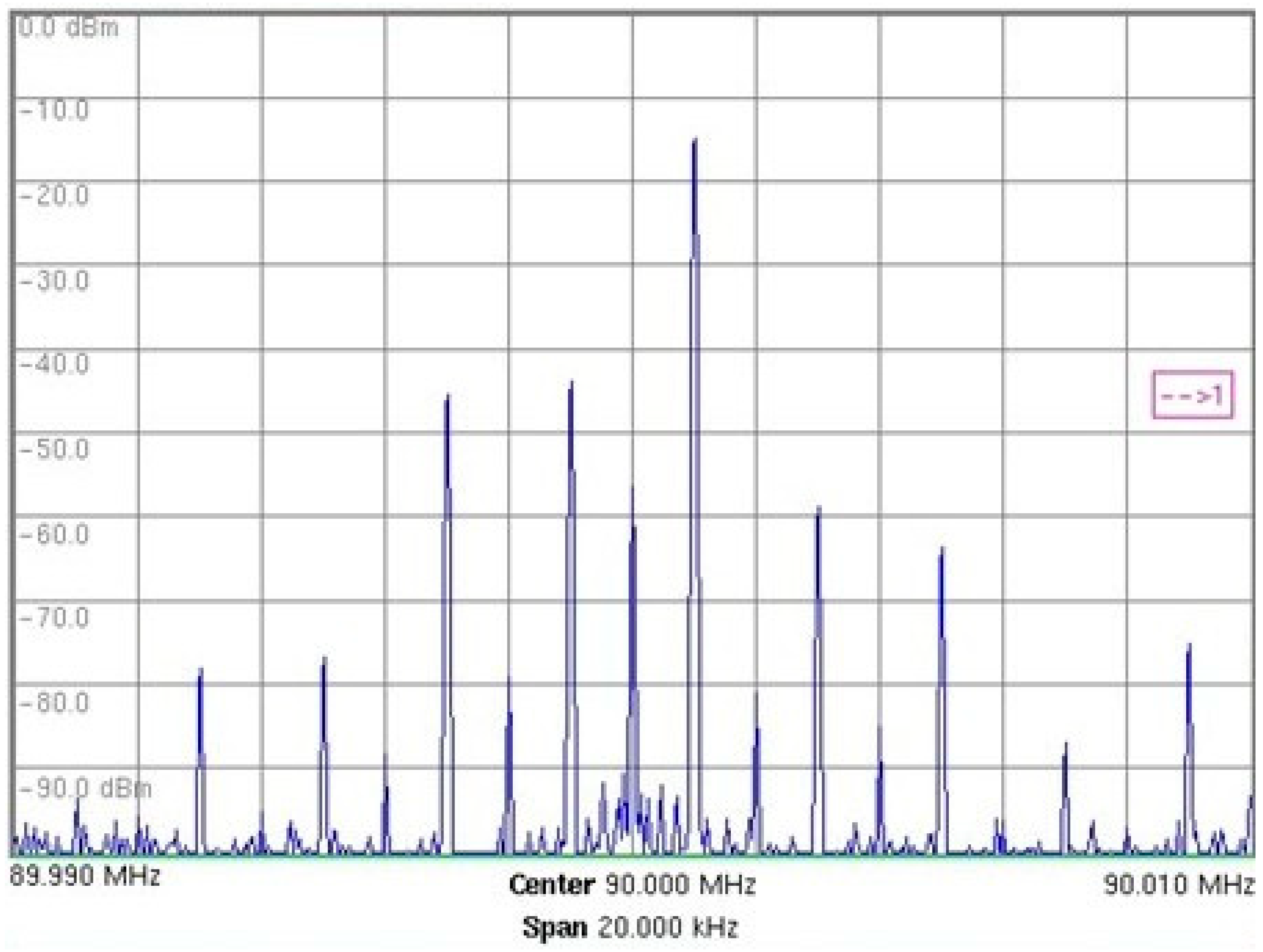
The generated output frequency at 90.001 MHz using a 90 MHz reference oscillator and a 1 kHz DDS signal in the USB setting shows many different harmonics and spurs (Figure 11). The suppression of these signals is at barely −30 dBc. The output power level of the RF signal is rather low (around −15 dBm). This requires an additional RF amplifier block at the output of the RF generator in order to fulfill the >0 dBm requirement. This will again consume the PCB area, mass, volume, and power. The frequency resolution depends on the resolution of the DDS inside the FPGA. Due to the small steps achievable in a DDS setup (see paragraph 4.2), the frequency resolution can be met easily.
It can be concluded that this design, although a valid approach for RF generation in space applications, has many drawbacks compared to the other discussed RF generation techniques.

4.4. DDS and DAC Chip Repackaging

A fourth option consists in repackaging an existing commercial off-the-shelf DDS-DAC integrated circuit. The technique offers a twofold benefit. On the one hand, this approach offers the functionality of the commercial device, and on the other hand it protects the chip against the harsh environment of space.
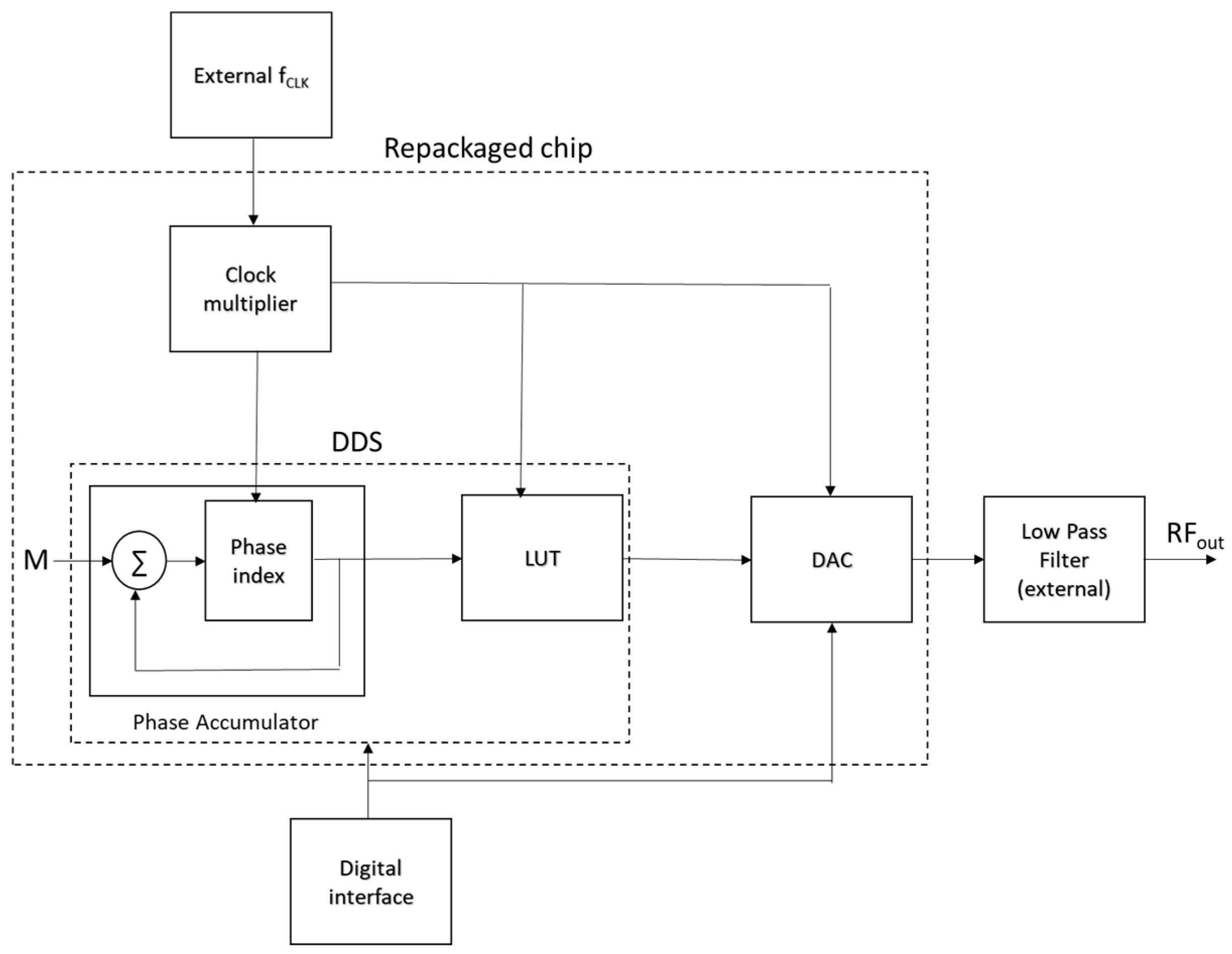
The principle in which the DDS is combined with a DAC is shown in Figure 12. An external clock signal fCLK is needed, as well as additional filtering of the output signal RFOUT and a digital interface.
The die of the chip is embedded in a space-resistant enclosure, for which specific repackaging techniques are available [43]. Several commercial devices exist that are able to fulfil the requirements listed in Table 1 and Table 2, e.g., AD9912 and the AD9957 from Analog Devices [44,45].
Commercial components are known for outgassing generation in the context of low pressures and high temperatures [46]. This could jeopardize a mission in which optical elements are used. Hence, care has to be taken if this approach is selected.

4.5. ASIC

Although not tested or simulated in the frame of this research, for the sake of completeness, the author would like to mention the technique of an Application-Specific Integrated Circuit (ASIC) in the frame of space applications [47,48,49]. In this approach, intellectual property cores are used from a space-qualified library and custom built in the ASIC [49,50]. The device is able to fully integrate the DDS, the DAC, the balun convertor, as well as the low-pass filter, described in Section 4.2. Hence, a single-chip approach is possible, using minimal PCB area, mass, volume, and power. The available market for building these ASICs for space applications is rather limited. The disadvantage of using such a technique is its very high cost, together with the long lead time due to the custom development process and possibly ITAR/EAR restrictions.

5. Discussion and Future Work

Several RF generation techniques were discussed, specifically regarding their usability for driving AOTFs in a space-based environment. The obtained results show a comparison between different RF generator techniques, all capable of fulfilling the imposed requirements. The proposed techniques all use Commercial-Off-The-Shelf available components, each having a space-grade counterpart available. This makes the practical conversion of the proposed techniques into a space-grade setup straight forward.
A comparison is made between the different RF generation principles. Based on the description in the previous subsections, Table 4 gives an overview of the pros and cons of each generation technique.
Further practical testing can be carried out, especially for the RF generation techniques using DDS and DAC chip repackaging and ASIC design. This is part of future work. Eventually, Artificial Intelligence (AI)-based RF control can help to improve the applied RF signal towards the transducer of the AOTF. Hence, the DE of the AOTF can be increased. Additionally, using Gallium Nitride (GaN)-based drivers can help in miniaturing the RF generator design and improving efficiency.

Funding

This research received no external funding.

Institutional Review Board Statement

Not applicable.

Data Availability Statement

The original contributions presented in the study are included in the article; further inquiries can be directed to the corresponding author.

Acknowledgments

The author would like to thank the Royal Belgian Institute for Space Aeronomy (BISA) and the Technical University of Delft (TU Delft) to make this study possible.

Conflicts of Interest

The author declares no conflicts of interest.

Abbreviations

The following abbreviations are used in this manuscript:
AIArtificial Intelligence
AOTFAcousto-Optical Tunable Filter
ASICApplication-Specific Integrated Circuit
COTSCommercial-Off-The-Shelf
DACDigital-to-Analog Convertor
DDSDirect Digital Synthesis
DEDiffraction Efficiency
ECSSEuropean Cooperation for Space Standardization
FPGAField Programmable Field Array
GaNGallium Nitride
KDPpotassium–dihydrogen–phosphate
LPFLow-Pass Filter
LSBLower Side Band
LUTLock-Up Table
NIRNear-Infrared
PCBPrinted Circuit Board
PFDPhase-Frequency Detector
PLLPhase-Locked-Loop
RFRadio Frequency
SSBSingle Side Band
TeO2Tellurium-Dioxide
UARTUniversal Asynchronous Receiver-Transmitter
USBUpper Side Band
UVUltra-Violet
VCOVoltage-Controlled Oscillator
VISVisible

References

  1. Mortensen, A.N.; Dyer, S.A.; Hammaker, R.M.; Fateley, W.G. A Hadamard-multiplexed spectrometer based on an Acousto-Optic Tunable Filter. IEEE Trans. Instrum. Meas. 1996, 45, 394–398. [Google Scholar] [CrossRef]
  2. Takahashi, H.; Masuda, C.; Gotoh, Y.; Koyama, J. Laser diode interferometer for vibration and sound pressure measurements. IEEE Trans. Instrum. Meas. 1989, 38, 584–587. [Google Scholar] [CrossRef]
  3. Vanhamel, J.; Dekemper, E.; Berkenbosch, S.; Clairquin, R. Novel Acousto-Optical Tunable Filter (AOTF) Based Spectropolarimeter for the Characterization of Auroral Emission. Instrum. Sci. Technol. 2021, 49, 245–257. [Google Scholar] [CrossRef]
  4. Errera, Q.; Dekemper, E.; Baker, N.; Debosscher, J.; Demoulin, P.; Mateshvili, N.; Pieroux, D.; Vanhellemont, F.; Fussen, D. On the capability of the future ALTIUS ultraviolet-visible-near-infrared limb sounder to constrain modelled stratospheric ozone. Atmos. Meas. Technol. 2021, 14, 4737–4753. [Google Scholar] [CrossRef]
  5. Gogoi, P.K.; Sharma, A.; Vanhamel, J.; Loicq, J. Investigating the Bounds of Quality Factor for Class-E Series-Tuned RF Power Amplifiers and Their Computer-Aided Optimization. Appl. Sci. 2024, 14, 11881. [Google Scholar] [CrossRef]
  6. Evdokimova, D.; Fedorova, A.; Ignatiev, N.; Korablev, O.; Montmessin, F.; Bertaux, J.-L. Near-Surface Water Vapor Content Based on SPICAV IR/VEx Observations in the 1.1 and 1.18 μm Transparency Windows of Venus. Atmosphere 2025, 16, 726. [Google Scholar] [CrossRef]
  7. Mantsevich, S.N.; Kostyleva, E.I.; Yushkov, K.B.; Molchanov, V.Y. Experimental observation of reflected acoustic beam tilting with temperature in quasi-collinear acousto-optic filters. Appl. Acoust. 2025, 233, 110632. [Google Scholar] [CrossRef]
  8. Dekemper, E.; Vanhamel, J.; Kastelik, J.-C.; Pereira, N.; Bolsée, D.; Cessateur, G.; Lamy, H.; Fussen, D. New AOTF-based instrumental concepts for atmospheric science. In Proceedings of the SPIE, Fourteenth School on Acousto-Optics and Applications, Torun, Poland, 24–27 June 2019. [Google Scholar]
  9. Xu, J.; Stroud, R. Acousto-Optic Devices: Principles, Design and Applications; Wiley: New York, NY, USA, 1992. [Google Scholar]
  10. Evdokimova, D.; Fedorova, A.; Ignatiev, N.; Zharikova, M.; Korablev, O.; Montmessin, F.; Bertaux, J.L. Cloud Opacity Variations from Nighttime Observations in Venus Transparency Windows. Atmosphere 2025, 16, 572. [Google Scholar] [CrossRef]
  11. Kim, S.; Jeong, T.-I.; Taylor, R.A.; Kyhm, K.; Kim, Y.-J.; Kim, S. Interleaved frequency comb by chip-scale acousto-optic phase modulation at polydimethylsiloxane for higher-resolution direct plasmonic comb spectroscopy. PhotoniX 2025, 6, 12. [Google Scholar] [CrossRef]
  12. Dekemper, E. Development of an AOTF-Based Hyperspectral Imager for Atmospheric Remote Sensing. Ph.D. Thesis, UCL, Louvain-la-Neuve, Belgium, 2014. [Google Scholar]
  13. Sun, S.; Zhao, H.; Guo, Q.; Wang, Y. Spatial-Dependent Spectral Response of Acousto-Optic Tunable Filters with Inhomogeneous Acoustic Distribution. Materials 2024, 17, 4537. [Google Scholar] [CrossRef]
  14. Vanhamel, J.; Dekemper, E.; Voloshinov, V.B.; Neefs, E.; Fussen, D. Electrical Bandwidth Testing of an AOTF Transducer as a Function of the Optical Diffraction Efficiency. J. Opt. Soc. Am. A Opt. Image Sci. Vis. 2019, 36, 1361–1366. [Google Scholar] [CrossRef] [PubMed]
  15. Yano, T.; Watanabe, A. Acoustooptic TeO2 tunable filter using faroff-axis anisotropic Bragg diffraction. Appl. Opt. 1976, 15, 2250–2258. [Google Scholar] [CrossRef]
  16. Goutzoulis, A.P.; Pape, D.R. Design of Acousto-Optic Deflectors, in Design and Fabrication of Acousto-Optic Devices; Marcel Dekker: New York, NY, USA; Basel, Switzerland; Hong Kong, China, 1994; pp. 69–122. [Google Scholar]
  17. Gupta, N.; Voloshinov, V.B. Development and characterization of two-transducer imaging acousto-optic tunable filters with extended tuning range. Appl. Opt. 2007, 46, 1081–1088. [Google Scholar] [CrossRef] [PubMed]
  18. Li, J.; Gui, Y.; Xu, R.; Zhang, Z.; Liu, W.; Lv, G.; Wang, M.; Li, C.; He, Z. Applications of AOTF Spectrometers in In Situ Lunar Measurements. Materials 2021, 14, 3454. [Google Scholar] [CrossRef]
  19. Prasad, N.S.; Trivedi, S.B.; Amarasinghe, P.; Jin, F.; Distler, M.; Kim, J.S.; Diener, H. Space Qualification Studies of AOTF Devices Under the MISSE-11 Mission. In Proceedings of the Proceedings Volume 12864, Solid State Lasers XXXIII: Technology and Devices, San Francisco, CA, USA, 27 January–1 February 2024. [Google Scholar]
  20. Korablev, O.I.; Trokhimovskiy, A.Y.; Kalinnikov, Y.K. AOTF spectrometers in space missions and their imaging capabilities. In Proceedings of the SPIE, Volume 10562, International Conference on Space Optics—ICSO 2016, 105621M, Biarritz, France, 18–21 October 2016. [Google Scholar]
  21. Vanhamel, J.; Berkenbosch, S.; Dekemper, E.; Leroux, P.; Neefs, E.; Van Lil, E. Testing of a possible RF-generator for a space based AOTF application in the frame of an ESA space mission. In Proceedings of the 2017 XXXIInd General Assembly and Scientific Symposium of the International Union of Radio Science (URSI GASS), Montreal, QC, Canada, 19–26 August 2017. [Google Scholar]
  22. Dekemper, E.; Fussen, D.; Van Opstal, B.; Vanhamel, J.; Pieroux, D.; Vanhellemont, F.; Mateshvili, N.; Franssens, G.; Voloshionv, V.; Janssen, C.; et al. ALTIUS: A Spaceborne AOTF-based UV-VIS-NIR Hyperspectral Imager for Atmospheric Remote Sensing. In Proceedings of the SPIE, Amsterdam, The Netherlands, 22–25 September 2014. [Google Scholar]
  23. Dekemper, E.; Vanhamel, J.; Van Opstal, B.; Fussen, D. The AOTF-based NO2 camera. Atmos. Meas. Technol. 2016, 9, 6025–6034. [Google Scholar] [CrossRef]
  24. Fussen, D.; Baker, N.; Debosscher, J.; Dekemper, E.; Demoulin, P.; Errera, Q.; Franssens, G.; Mateshvili, N.; Pereira, N.; Pieroux, D.; et al. The ALTIUS atmospheric limb sounder. J. Quant. Spectrosc. Radiat. Transf. 2019, 238, 106542. [Google Scholar] [CrossRef]
  25. Korablev, O.I.; Belyaev, D.A.; Dobrolenskiy, Y.S.; Trokhimovskiy, A.Y.; Kalinnikov, Y.K. Acousto-optic tunable filter spectrometers in space missions [invited]. Appl. Opt. 2018, 57, 119. [Google Scholar] [CrossRef]
  26. Mestice, M.; Neri, B.; Ciarpi, G.; Saponara, S. Analysis and Design of Integrated Blocks for a 6.25 GHz Spacefibre PLL. Sensors 2020, 20, 4013. [Google Scholar] [CrossRef]
  27. Texas Instruments, LMX2694. Available online: https://www.ti.com/product/LMX2694-EP (accessed on 16 March 2025).
  28. Nevejans, D.; Neefs, E.; Van Ransbeeck, E.; Berkenbosch, S.; Clairquin, R.; De Vos, L.; Moelans, W.; Glorieux, S.; Baeke, A.; Korablev, O.; et al. Compact high-resolution spaceborne echelle grating spectrometer with acousto-optical tunable filter based order sorting for the infrared domain from 2.2 to 4.3 μm. Appl. Opt. 2006, 45, 5191–5206. [Google Scholar] [CrossRef] [PubMed]
  29. Neefs, E.; Vandaele, A.C.; Drummond, R.; Thomas, I.R.; Berkenbosch, S.; Clairquin, R.; Delanoye, S.; Ristic, B.; Maes, J.; Bonnewijn, S.; et al. NOMAD spectrometer on the ExoMars trace gas orbiter mission: Part 1—Design, manufacturing and testing of the infrared channels. Appl. Opt. 2015, 54, 8494–8520. [Google Scholar] [CrossRef]
  30. Aranda, L.A.; Garcia-Herrero, F.; Esteban, L.; Sánchez-Macián, A.; Maestro, J.A. Radiation Hardened Digital Direct Synthesizer With CORDIC for Spaceborne Applications. IEEE 2020, 8, 83167–83176. [Google Scholar] [CrossRef]
  31. Analog Devices, Fundamentals of Direct Digital Synthesis (DDS), Tutorial MT-085. Available online: https://www.analog.com/media/en/training-seminars/tutorials/MT-085.pdf (accessed on 15 December 2024).
  32. Goldberg, B.G. Digital Frequency Synthesis Demystified; LLH Technology Publishing: Eagle Rock, VA, USA, 1999. [Google Scholar]
  33. Texas Instruments, DAC5675A-SP Radiation-Tolerant, 14-Bit, 400-MSPS Digital-to-Analog Converter. Available online: https://www.ti.com/lit/ds/symlink/dac5675a-sp.pdf (accessed on 16 January 2025).
  34. Xilinx, Virtex-4 Family Overview. Available online: https://www.xilinx.com/support/documentation/data_sheets/ds112.pdf (accessed on 15 January 2025).
  35. Microchip, RTAX™ Radiation-Tolerant FPGAs. Available online: https://www.microchip.com/en-us/products/fpgas-and-plds/radiation-tolerant-fpgas/rtax-s (accessed on 10 February 2025).
  36. Microchip, RTG4TM Radiation-Tolerant FPGAs. Available online: https://www.microchip.com/en-us/products/fpgas-and-plds/radiation-tolerant-fpgas/rtg4-radiation-tolerant-fpgas (accessed on 10 February 2025).
  37. NanoXplore, SoC FPGAs for Space. Available online: https://www.nanoxplore.com (accessed on 1 March 2025).
  38. Analog Devices, AD8001S. Available online: https://www.analog.com/en/products/ad8001s.html#product-overview (accessed on 5 March 2025).
  39. Beasley, J.S.; Miller, G.M. Modern Electronic Communication, 9th ed.; Pearson Prentice Hall: Upper Saddle River, NJ, USA; Columbus, OH, USA, 2008. [Google Scholar]
  40. Counselman, C.C.; Hinteregger, H.F. Digital single sideband mixer. IEEE 1973, 61, 478–479. [Google Scholar] [CrossRef]
  41. Liu, D.; Hu, A.; Zhang, K. A Quadrature Single Side-Band Mixer with Passive Negative Resistance in Software-Defined Frequency Synthesizer. Sensors 2018, 18, 3455. [Google Scholar] [CrossRef] [PubMed]
  42. Vanhamel, J.; Fussen, D.; Dekemper, E.; Neefs, E.; Van Opstal, B.; Pieroux, D.; Maes, J.; Van Lil, E.; Leroux, P. RF-driving of acoustic-optical tunable filters; design, realization and qualification of analog and digital modules for ESA. Microelectron. Reliab. 2015, 55, 2103–2107. [Google Scholar] [CrossRef]
  43. Aguirre, F.; Schatzel, D. High density packaging technologies for RF electronics in small spacecraft. In Proceedings of the IEEE Aerospace Conference Proceedings, Big Sky, MT, USA, 4–11 March 2017. [Google Scholar]
  44. Analog Devices, AD9912. Available online: https://www.analog.com/en/products/ad9912.html (accessed on 15 March 2025).
  45. Analog Devices, AD9957. Available online: https://www.analog.com/en/products/ad9957.html (accessed on 15 March 2025).
  46. McCluskey, P.; Mensah, K.; O’Conner, C.; Gallo, A. Reliable Use of Commercial Technology in High Temperature Environments. Microelectron. Reliab. 2000, 40, 1671–1678. [Google Scholar] [CrossRef]
  47. Waltham, N.; Morrissey, Q.; Clapp, M.; Bell, S.; Jones, L.; Torbet, M. The Design and Development of Low- and High-Voltage ASICs for Space-Borne CCD Cameras. CEAS Space J. 2017, 9, 517–529. [Google Scholar] [CrossRef]
  48. Sordo-Ibanez, S.; Pinero-Garcia, B.; Munoz-Diaz, M.; Ragel-Morales, A.; Ceballos-Caceres, J.; Carranza-Gonzaez, L.; Espejo-Meana, S.; Arias-Drake, A.; Ramos-Martos, J.; Mora-Gutiérrez, J.M.; et al. A Front-End ASIC for a 3-D Magnetometer for Space Applications by Using Anisotropic Magnetoresistors. IEEE Trans. Magn. 2015, 51, 1–4. [Google Scholar] [CrossRef]
  49. Gandola, M.; Grassi, M.; Mele, F.; Bertuccio, G.; Malcovati, P. Mixed-Signal ASICs for X- and γ-Ray Spectroscopy in Space Applications. In Proceedings of the 26th IEEE International Conference on Electronics, Circuits and Systems (ICECS), Genoa, Italy, 27–29 November 2019. [Google Scholar]
  50. Barr, K.E. ASIC Design in the Silicon Sandbox, a Complete Guide to Building Mixed-Signal Integrated Circuits; McGraw-Hill Education: New York, NY, USA, 2006. [Google Scholar]
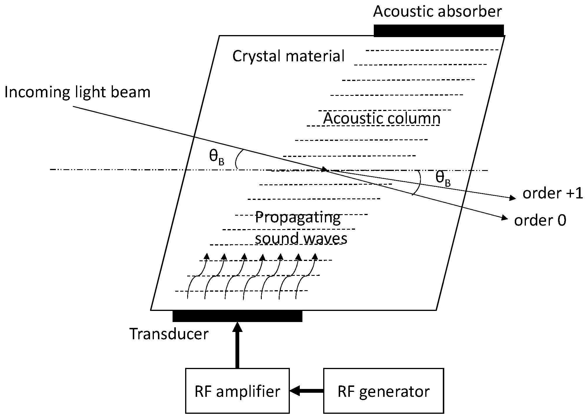
Figure 1. The setup of the AOTF, together with the RF driving system, applied to the transducer. Reproduced and adapted with permission from reference [14] by OSA Publishing.
Applsci 15 08739 g001
Figure 2. PLL principle.
Applsci 15 08739 g002
Figure 3. LMX2694 PLL outline for space applications.
Applsci 15 08739 g003
Figure 4. LMX2694 PLL output spectrum at 100 MHz.
Applsci 15 08739 g004
Figure 5. LMX2694 PLL output power level for different current settings (0 up to 63).
Applsci 15 08739 g005
Figure 6. DDS principle.
Applsci 15 08739 g006
Figure 7. DDS RF generator setup—Virtex4/DAC5675A-SP.
Applsci 15 08739 g007
Figure 8. DDS RF generator harmonics and spur levels for different frequencies.
Applsci 15 08739 g008
Figure 9. SSB principle.
Applsci 15 08739 g009
Figure 10. SSB setup for the VIS range.
Applsci 15 08739 g010
Figure 11. SSB output signal for the VIS range.
Applsci 15 08739 g011
Figure 12. Principle of the DDS and DAC combination, repacked into one chip.
Applsci 15 08739 g012
Table 1. RF generator general requirements.
General RequirementsValueUnit
Unwanted spectral component suppression<−30dB
Accuracy1kHz
Resolution5kHz
Long term stability (10 s)5kHz
Stabilization time<5ms
Output power uncertainty1mW
Nominal load50Ohm
Output power level> 0dBm
Table 2. RF generator specific requirements (depending on the optical domain VIS/NIR/UV).
Specific Requirements (Optical Domain Specific)ValueUnit
Frequency range (VIS domain)60–120 MHz
Power level (VIS domain)0.3W
Frequency range (NIR domain)45–90 MHz
Power level (NIR domain)0.3W
Frequency range (UV domain)125–250 MHz
Power level (UV domain)3W
Table 3. RF generator techniques and type classification.
RF Generator Technique Type
Integrated PLL designAnalog
DDS inside an FPGADigital
SSB mixingAnalog
DDS and DAC chip repackagingDigital
ASICDigital
Table 4. RF generator techniques comparison table.
RF Generation TechniqueAdvantagesDisadvantages
Integrated PLL
design
-
fully digital design
-
low mass
-
low PCB area usage
-
compliant with requirements
-
output filtering needed
-
limited flight heritage
DDS inside an FPGA
-
proven digital design
-
flight heritage
-
compliant with VIS and NIR frequency range)
-
for UV frequency range, a frequency doubler is needed
-
output filtering needed
-
complex PCB design with FPGA
SSB mixing
-
proven analog design
-
compliant with requirements
-
complex output filtering is needed
-
complex design
-
high power consumption
-
high PCB area usage
-
high mass
-
low output power level
-
harmonic suppression < −30 dBc is marginally achieved
DDS and DAC chip repackaging
-
fully digital design
-
compliant with the requirements
-
high cost
-
possible outgassing issues
ASIC
-
fully digital design
-
low mass
-
low PCB area usage
-
compliant with requirements
-
very high cost
-
limited market available
-
long lead time
-
ITAR/EAR restrictions
Disclaimer/Publisher’s Note: The statements, opinions and data contained in all publications are solely those of the individual author(s) and contributor(s) and not of MDPI and/or the editor(s). MDPI and/or the editor(s) disclaim responsibility for any injury to people or property resulting from any ideas, methods, instructions or products referred to in the content.