1. Introduction
Soldering remains one of the most widely used technologies for joining components in the power electronics industry due to its simplicity and efficiency in mass production. It plays a vital role in ensuring reliable electrical connections, particularly in high-power applications. To enhance the quality and durability of solder joints, protective atmospheres, such as forming gas, forming acid, or vacuum conditions, are often employed to optimize soldering interfaces [
1].
Achieving strong and durable soldering connections requires proper wettability and effective oxide removal from both the soldering alloy and the substrate. These objectives are typically accomplished using a liquid flux, a chemical agent that facilitates bonding. Conventional soldering techniques that employ flux-containing soldering pastes for oxide removal and surface cleaning [
2] require additional cleaning steps to eliminate flux residues. These residues, if not removed, can lead to corrosion and interfere with subsequent processes, such as wire bonding. However, these extra steps can compromise manufacturing efficiency and add to the overall complexity and cost of production [
3,
4,
5]. However, flux residues must be removed post-soldering due to their corrosive effects, which can lead to the long-term degradation of electronic components [
6].
Traditionally, rosin-based fluxes have been cleaned using halogenated or chlorofluorocarbon solvents. While effective, these solvents pose environmental hazards, contributing to ozone depletion, and are classified as carcinogenic substances. Increasing regulatory restrictions on hazardous chemicals may lead to their phasing out in the near future. Consequently, researchers are exploring alternative flux formulations that minimize ecological impacts while maintaining soldering quality. Non-clean soldering pastes are designed to eliminate the need for post-soldering cleaning by allowing for flux residues to remain on the board. However, these formulations come with potential drawbacks, such as flux-spattering and solder splashes, which can lead to unintended contamination and damage to sensitive components, including diodes and insulated-gate bipolar transistors (IGBTs). While non-clean fluxes reduce the risk of electrochemical migration, water-soluble fluxes tend to be more chemically active, necessitating thorough cleaning to ensure long-term reliability [
7,
8,
9,
10,
11].
Recent research has focused on the development of fluxless soldering technologies, an innovative approach with significant market potential. Fluxless soldering eliminates the need for a liquid flux by utilizing alternative oxide removal methods. Various reducing atmospheres, such as hydrogen gas, forming gas (a nitrogen–hydrogen mixture), and formic acid (HCOOH), are employed to achieve this aim [
12,
13].
While pure hydrogen is an effective reducing agent, its application at 300 °C is impractical for most soldering processes in the electronics industry. To circumvent this limitation, forming gas is used as an alternative. By diluting hydrogen with inert gases (primarily nitrogen), the hydrogen concentration remains below 5.7%—the threshold for spontaneous combustion. To ensure safe handling, gas suppliers typically provide forming gas with hydrogen concentrations of 4.0% or 5.0%. Another promising fluxless soldering technique involves the use of formic acid, a simple organic acid with efficient oxide removal capabilities. In its gaseous state, formic acid can adsorb onto metal surfaces and undergo decomposition into hydrogen (H) and formate ions (HCOO). At temperatures of approximately 200 °C, formate ions further decompose into hydrogen and carbon dioxide (CO
2). The hydrogen generated from this reaction actively interacts with metal oxides, reducing them to metallic elements while producing CO
2 and water vapor (H
2O) [
14,
15,
16,
17,
18].
Tin-based solders are the most commonly used alloys in the electronics industry. Their oxide films primarily consist of tin monoxide (SnO) and tin dioxide (SnO
2). The chemical reaction between formic acid and tin oxides can be described as follows:
At temperature above 150 °C,
Formic acid becomes carbon dioxide and hydrogen in the thermal cleaning (reflow) process. By employing advanced fluxless soldering methods, manufacturers can enhance the efficiency, reduce the environmental hazards, and improve the reliability of electronic assemblies. This emerging technology holds great promise in the evolution of sustainable and high-performance soldering processes.
2. Void Classification
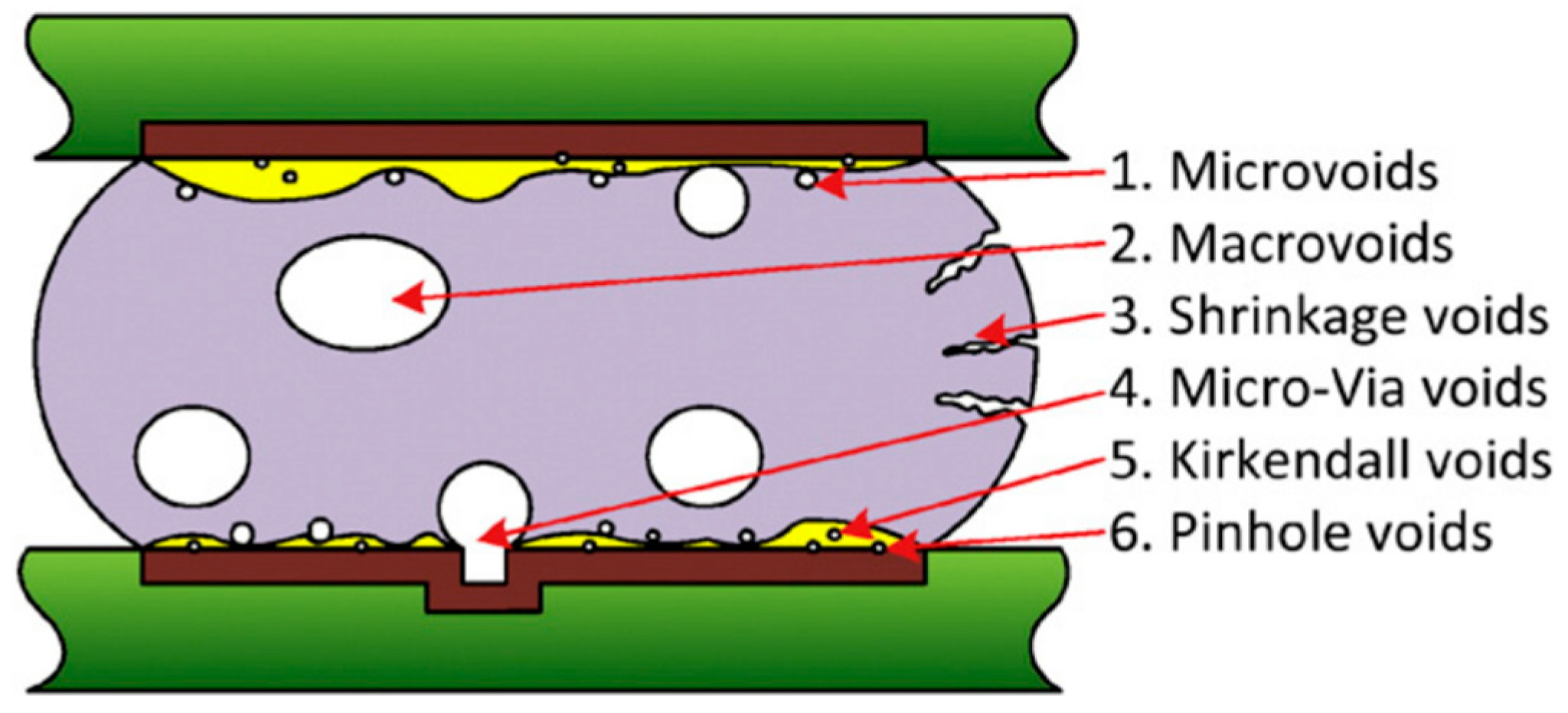
Voids are non-conductive cavities in the soldered joint, and they can pose a reliability risk, especially for power electronics where higher currents are present. Voids are formed during the soldering process; their presence can decrease heat dissipation from the product to the heatsink, which results in the non-uniform thermal stress, lower lifetime, or thermal breakdown of the products. Voids can be classified into several categories: macrovoids, microvoids, shrinkage voids, voids in microvoids, Kirkendall voids, and pinhole voids. The typical macrovoid diameter varies between 100 µm and 300 µm. Voids with diameters below 50 µm are considered to be microvoids. Voids with diameters between 50 µm and 100 µm are sometimes referred to as microvoids as well, or sometimes as macrovoids, and there is no clear agreement on how to classify these void sizes. Shrinkage voids or solidification voids are the consequence of the reduction in volume that occurs when a solder changes its state from liquid to solid [
19].
By applying a vacuum while the solder is in the liquid phase, most of the voids can be sucked out of the soldering joint [
20,
21]. More critical are non-wetted areas, due to residues on the substrate or components, which drastically reduce the contact area for electrical and thermal transfer. Reasons for the existence of these residues can be contamination, inadequate handling of the substrate and components, inadequate cleaning, or inappropriate process parameters [
22,
23,
24].
De-wetting refers to the failure of molten solder to establish a proper metallic bond with the base metal. This condition occurs when the solder initially wets the surface but then retracts, leaving behind irregularly shaped solder mounds separated by areas covered with a thin solder film and exposed base metal. Notably, the surface finish remains unexposed. A common cause of de-wetting is oxidation on the surface to be soldered. Oxide layers act as a barrier between the solder and the base metal, and prevent effective adhesion. When oxidation is widespread, non-wetting can occur across the entire oxidized surface [
25,
26].
Solder Joint Inspection Methods
Visual inspection methods are not sufficient because the solder joints are covered by the connected components, and, therefore, more sophisticated tools must be used for the inspection.
X-ray inspection utilizes high-frequency electromagnetic radiation generated using an X-ray tube. These rays are emitted as a fanned beam from a point source, penetrate the specimen, and are captured on the opposite side using an X-ray detector. As the X-ray photons pass through the material, they interact with its internal structure. This technique leverages the penetrating ability of X-rays to identify issues such as an insufficient solder, poor soldering, solder shortages, and other defects in the solder joints.
When defects like porosity, slag inclusion, or incomplete soldering are present, they appear as bright spots or lines in the affected areas. Visually, these defects can be identified by their brightness compared to the surrounding background in the inspection image. From an image-processing perspective, defects are detected based on variations in pixel gray values within the image.
The visibility of these features depends on the material’s density and atomic number: higher values increase the likelihood of X-ray interaction. The X-ray detector captures all unabsorbed photons in a planar resolution, converting the specimen’s volumetric information into a two-dimensional (2D) image.
SAM utilizes high-frequency acoustic waves, typically ranging from 15 to 300 MHz, to examine both the surface and internal structure of materials. A transducer generates a focused acoustic wave, which is directed at the specimen submerged in water, serving as the coupling medium.
As the acoustic wave penetrates the specimen, it interacts with the material in several ways: it may be partially absorbed, scattered by fine internal structures, or reflected at interfaces between different materials. These interactions depend on variations in acoustic impedance, which are influenced by the material’s density and the speed of sound within it.
Reflections caused by an interface vertical to the wave propagation direction are reflected straight back, and the transducer records the echo time resolved, holding several interface reflections with different signal propagation delays, also known as time of flight, which is a key feature in SAM. Unlike X-ray imaging, SAM is capable of detecting internal defects such as cracks and delamination. These defects represent separations within the material that cause strong acoustic reflections due to the abrupt transition from solid material to air, gas, or a vacuum—even when the gap is extremely small. This sensitivity allows for SAM to identify flaws that may go undetected when using X-ray methods.
3. Experimental Method
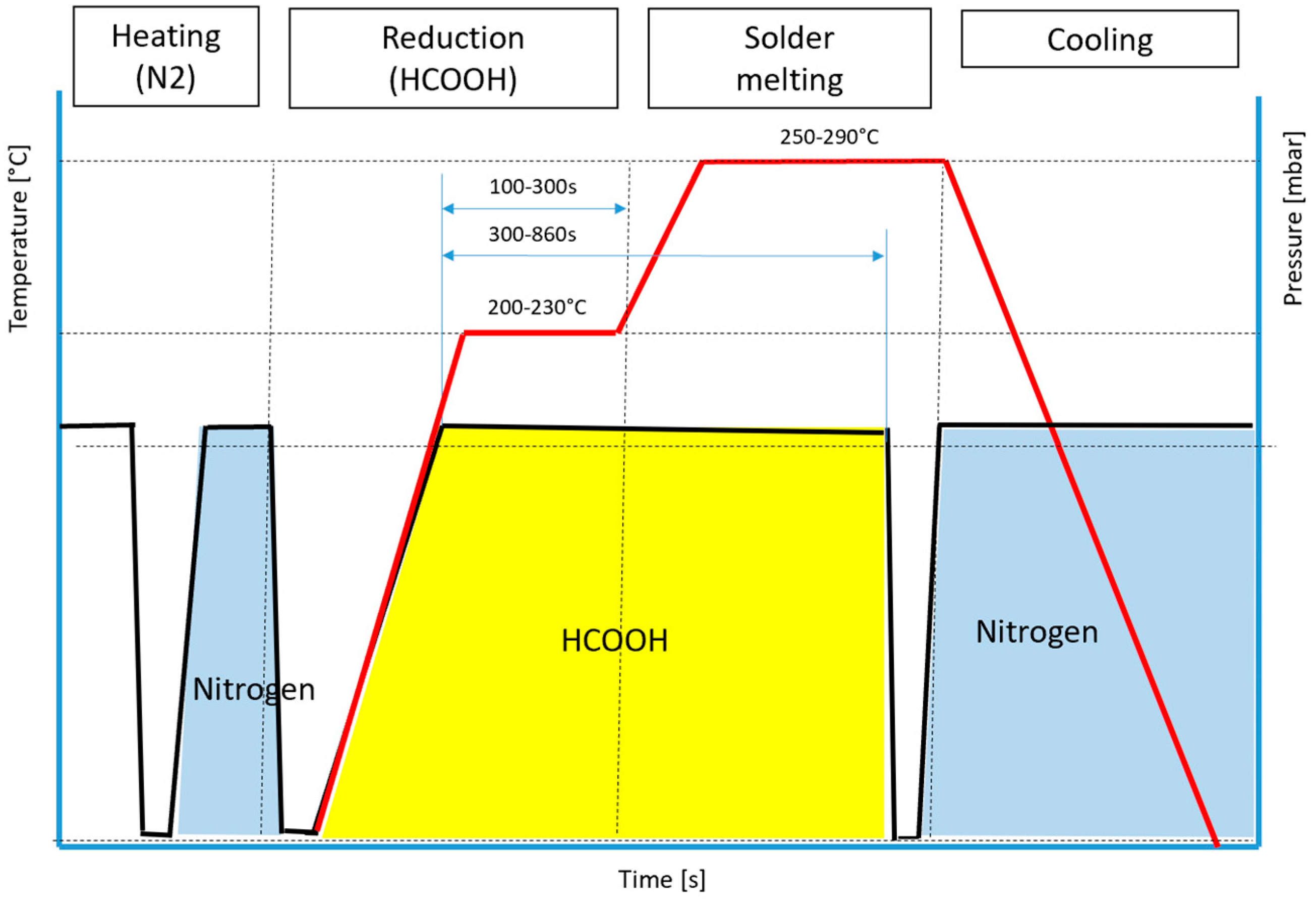
Soldering tests were performed in the PINK VADU300XL vacuum reflow furnace with the possibility to use formic acid as the reduction atmosphere in the first and second processing chamber. The first chamber is usually used for pre-heating and surface activation with HCOOH; the second chamber is used for soldering (solder melting); and the third chamber is used for cooling the product (
Figure 1). Analysis and sample evaluation were performed with a VUE 250-p scanning acoustic microscope with a 25 MHz transducer. For all tests, we used nickel-galvanized Cu baseplates and a highly reliable solder alloy from four different suppliers (
Table 1). Reduction atmosphere was created with nitrogen flowing through the bubbler with formic acid (>98%).
The aim of the soldering test was to compare soldering materials with the same composition from various suppliers. For reference, “Supplier A” is used within actual production, which complies with the defined process quality and capability. For evaluation, three other different suppliers were tested, also, and were compared with different material lots from “Supplier A”.
The initial soldering test was performed in PINK VADU300XL from 120 s up to 860 s of HCOOH cleaning with dummy DCBs (a test without IGBT or Diode chips). Later on, full samples with chips were assembled as well.
The soldering process consisted of preheating and cleaning the baseplate and highly reliable solder. Subsequently, the samples were heated to the soldering temperature, ensuring that the solder melted. The soldering process ended by gradually cooling it to ambient temperature. An important factor that affects the properties of soldering is the temperature (duration at temperature), along with the cleaning time duration of the HCOOH in the heating and soldering chambers.
During the soldering process, specific temperature ranges were strategically selected to optimize the efficiency and quality of the soldering operation (
Figure 2). The preheating phase involved temperatures ranging from 180 °C to 250 °C, which are crucial for preparing the materials for soldering. This step ensures that the base materials are sufficiently heated and cleaned to facilitate the subsequent soldering process. Within this temperature range, the chamber undergoes a chemical reaction, where HCOOH plays a vital role in reducing oxides. The presence of oxides can impede the soldering process by creating barriers that prevent proper bonding. Therefore, HCOOH acts as a reducing agent, effectively removing these oxides and enhancing the quality of the soldered joints.
Following preheating, the soldering phase is conducted at temperatures between 240 °C and 290 °C. This range was carefully chosen to ensure that the solder melted and flowed adequately, forming strong, reliable connections between components. Precise control of the temperature during this phase is essential to achieve optimal soldering results and prevent issues, such as cold solder joints or overheating, which can damage the components.
Additionally, the cleaning time within the chamber, ranging from 50 to 860 s, is a critical parameter. This duration allows for thorough cleaning of the chamber environment, ensuring that any residual contaminants or oxides are effectively removed. The cleaning process is vital for maintaining the integrity of the soldering environment, as it prevents contamination that could adversely affect the quality and reliability of the soldered connections. By carefully managing these temperature ranges and cleaning times, the soldering process can achieve high-quality results with enhanced durability and performance.
In the upcoming soldering experiment (
Figure 3), three distinct levels of substrate temperature (200 °C, 215 °C, and 230 °C) were selected for the introduction of vapor into the chamber. Additionally, three varied durations were chosen for the cleaning (100 s, 200 s, and 300 s) of surfaces once atmospheric pressure was achieved. These parameters are crucial for determining the optimal conditions under which the vapor interacts with the substrate, ensuring effective cleaning and preparation for soldering. By experimenting with different temperature levels and cleaning durations, the process aims to identify the most efficient combination that enhances the quality and reliability of the soldered connections.
Substrate temperature was measured in each chamber of the PINK furnace with 4 thermocouples connected to the soldering carrier from the bottom side; however, the substrate temperature is different to the real temperature measured on the module assembly. To determine the actual temperature on the copper baseplate, thermocouples need to be fixed on the baseplate and measured during the reflow process. The main goal of the experiment was to identify the process parameters that have the main influence on the measured void area.
Figure 3 illustrates that the most effective reduction in void area was obtained with extended activation time and elevated temperature during the formic acid treatment. This comparison involved a series of eleven experimental runs (with different parameter settings), with each run comprising the soldering of eight modules. The results highlight the significant impact of both activation duration and temperature on minimizing voids, thereby improving the overall quality of the soldered connections.
As the duration within the reduction atmosphere extended, there was a notable decrease in voids within the solder joint, reaching a minimal percentage of the Direct Copper Bonded (DCB) area (
Figure 3, Group 5, orange color). This observation suggests that longer exposure to the formic acid environment effectively mitigates void formation, potentially indicating the presence of surface contamination on the materials being joined. The prolonged interaction with formic acid appears to enhance the cleaning process, allowing for the more thorough removal of contaminants that could otherwise contribute to void formation. The better the reduction number of the void area, the better performance operation that the power semiconductor module can be expected to achieve naturally. Therefore, our recommendation for industrial applications is to perform 300 s of cleaning time at 230 °C.
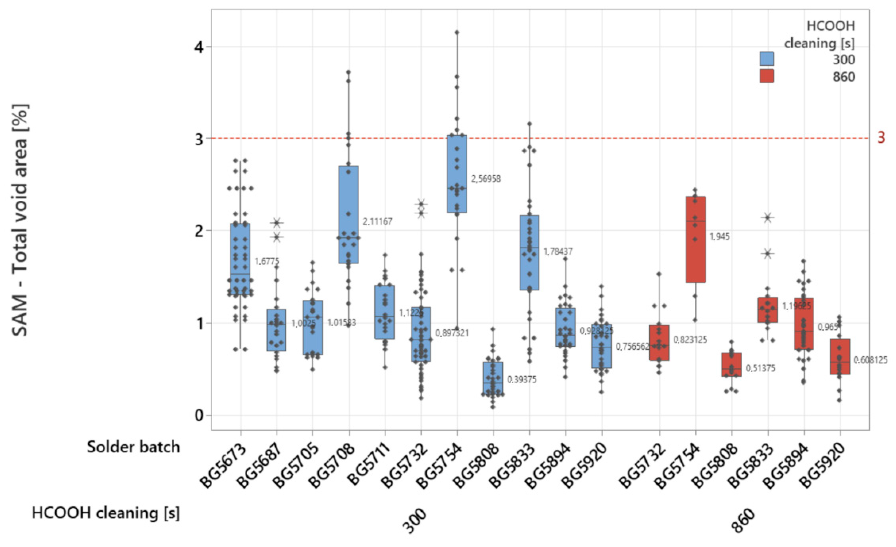
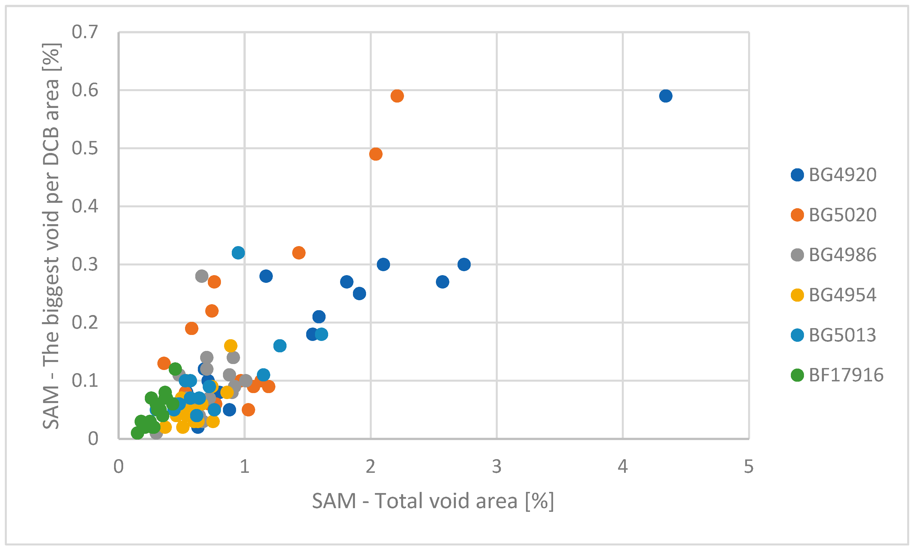
To verify the input material quality and surface impurities’ impacts, various solder batches were tested as well (
Figure 4) for different formic acid cleaning times. Higher impacts from the solder preforms’ surface quality can be seen when lowering the cleaning time to 300 s, where the tested batches have higher values for their average void areas (BG5673—1.6775%, BG5687—1.0025%, BG5705—1.01533%, BG5708—2.11167%, BG5711—1.1225%, BG5732—0.897321%, BG5754—2.56958%, GB5808—0.39375%, BG5833—1.78437%, BG5894—0.928125% and BG5920—0.756562%). The impact of improved cleaning time is more visible for times up to 860 s, where the soldering process is more stable and the average void drops below 1%. In a comparison of the same test batches, the overall values are similar (BG5732—0.823125%, BG5808—0.51375%, BG5894—0.969%, BG5920—0.608125%). For the test samples with higher values, they have increased cleaning time, showing a positive impact with reductions in total void area for BG5754—1.945% and BG5833—1.19625%. To better quantify the impact of cleaning time on processing time and average void area, cleaning tests from 200 s up to 600 s were performed as well (
Figure 5) to find out the minimal stable process requirements (
Figure 6 and
Figure 7).
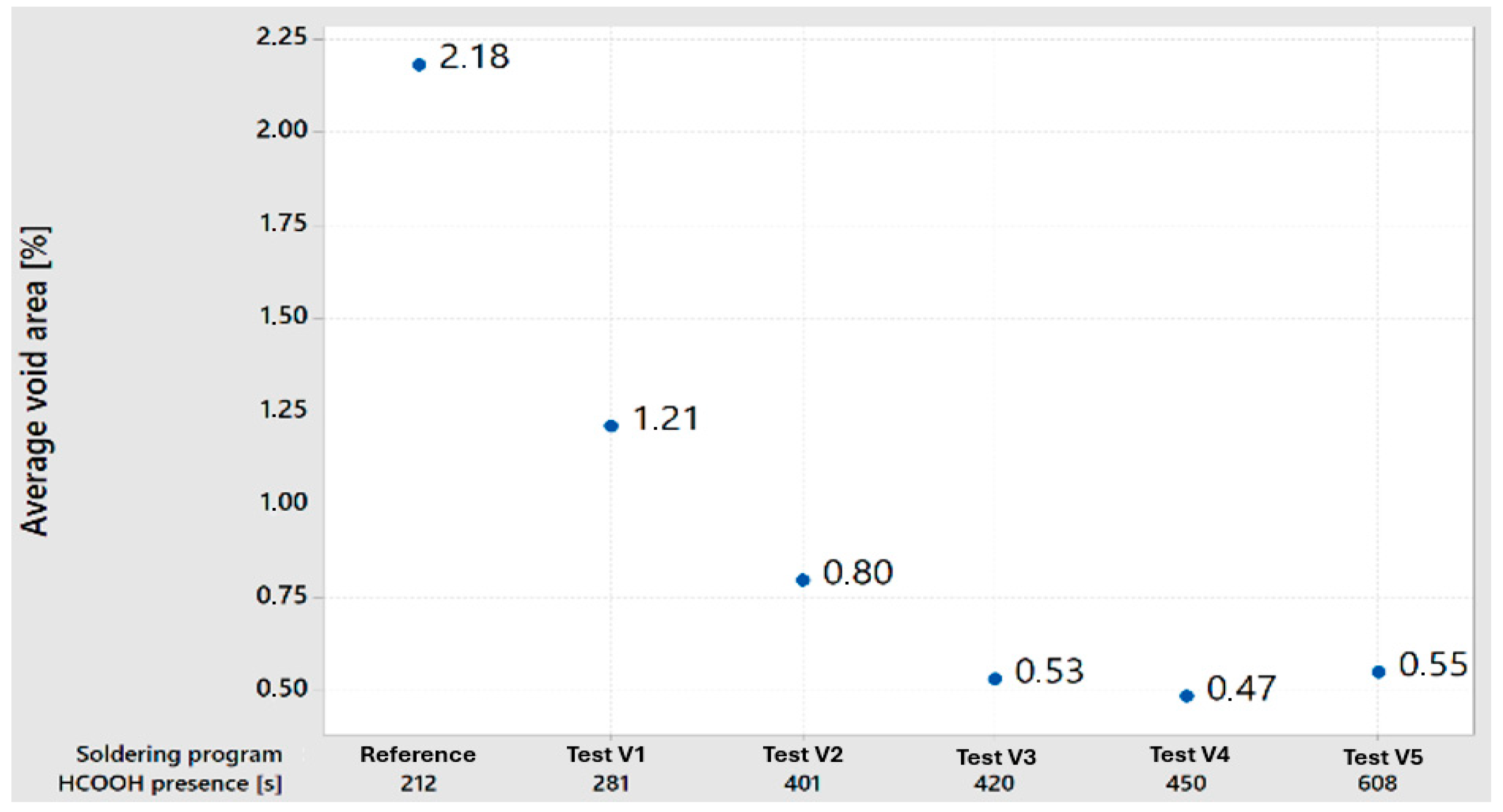
Higher formic acid HCOOH presence has a direct impact on cleaning the materials during the soldering process. As for the selected reference group and process settings, there is a visible improvement visible when decreasing the average void area. In comparison to the reference group, an extended time of 281 s decreased average void ratios to 1.21%, and, with a cleaning time of 401 s, to 0.8%. Higher cleaning times than 420 s (420 s, 450 s, and 608 s) have, for average void areas, similar results (0.53%, 0.47%, and 0.55%), which represents a virtual boundary for cleaning process stabilization.
Moreover, the increase in temperature during this process plays a crucial role in accelerating the chemical reaction between formic acid and metal oxides. Higher temperatures enhance the reactivity of formic acid, facilitating a more efficient breakdown of oxides and other impurities on the metal surfaces. This accelerated reaction not only aids in reducing voids, but also improves the overall quality and reliability of the solder joints. By optimizing both the duration and temperature of formic acid exposure, the soldering process can achieve superior results with minimal void presence, ensuring robust and durable connections between components. This approach underscores the importance of precise control over environmental conditions to enhance the effectiveness of soldering operations.
Prior to the oxide removal process, the metal surfaces were prepared using a controlled etching methodology to ensure uniform exposure and enhance the effectiveness of subsequent treatments. This preparation step involved the application of a mild acid solution to remove surface contaminants and native oxides, creating a clean and reactive surface for formic acid treatment. The experimental results demonstrate that the oxide removal process using formic acid is time-dependent. As the exposure time increases, the removal of thick metal oxides becomes significantly more effective, indicating a strong correlation between treatment duration and oxide reduction efficiency.
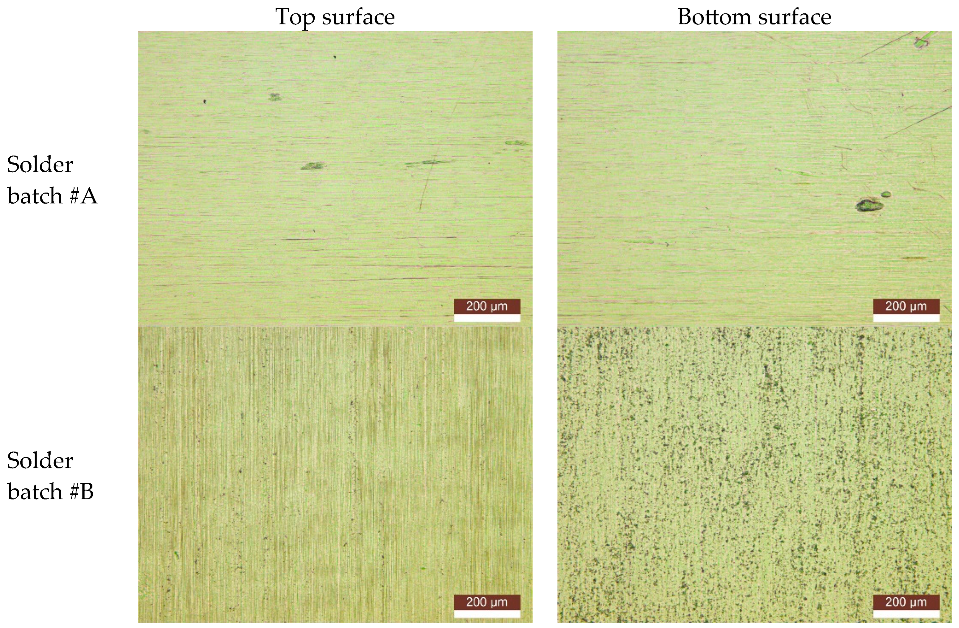
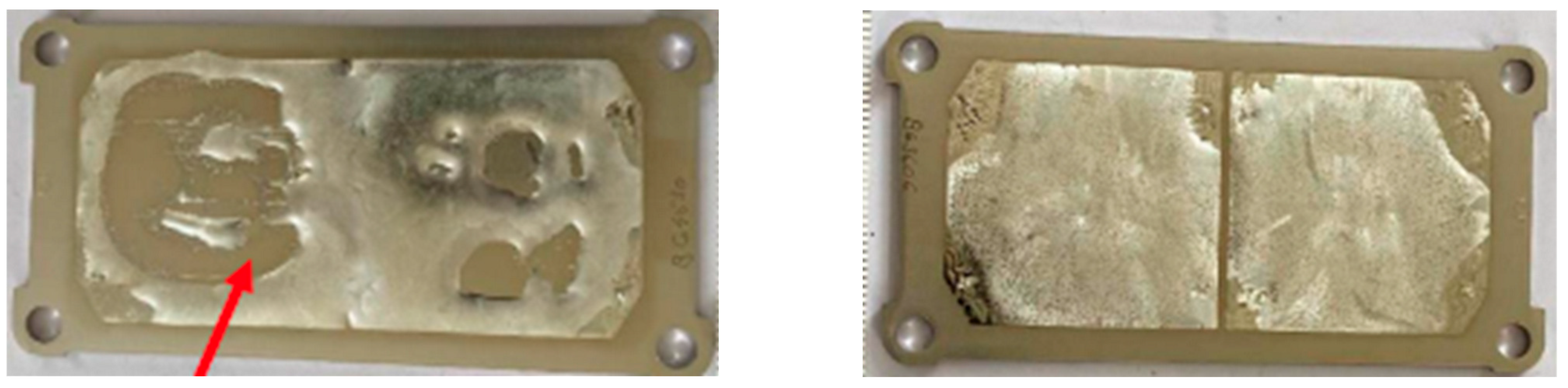
We can assume that no contamination in the volume of solder is present because formic acid vapor can sufficiently remove the oxide layer only from the surface. Different surface structures of solder preforms were observed with the optical Microscop LEICA DM4M. In general, surfaces with many pinholes and valleys showed worse wetting behavior and void ratios after soldering compared to surfaces with lower roughness. Solder preforms of the desired thickness are manufactured using the multiple rolling processes, which could have an impact of the surface’s roughness. Rough surfaces (
Figure 8, solder batch #B) tend to oxidize more, and oxides from production could be entrapped in the cavities under the surface, where formic acid cannot reach and remove them (
Figure 9 and
Figure 10).
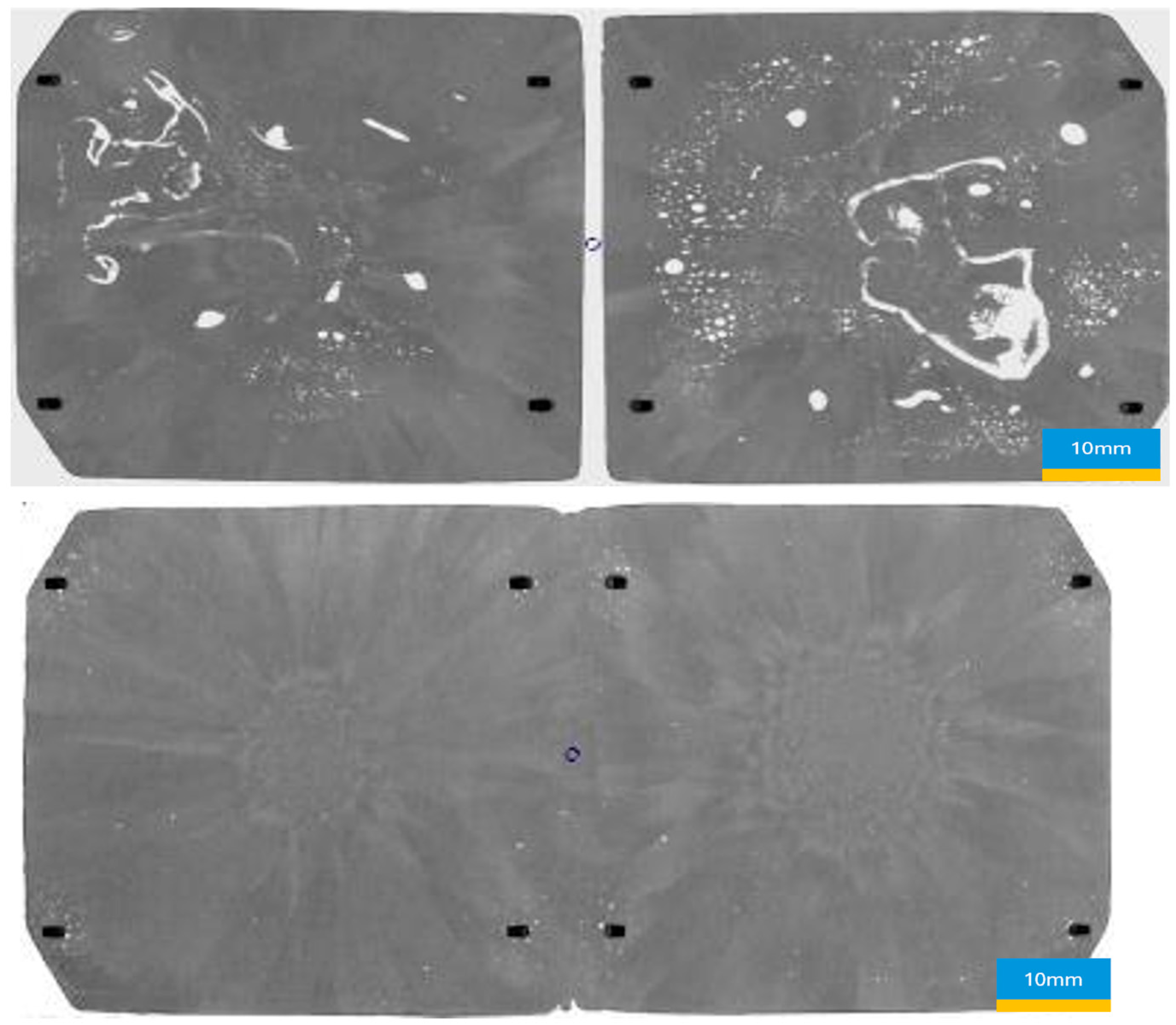
The soldering experiment results provide insightful data on the effectiveness of varying durations of formic acid’s presence in reducing void areas within soldered units (
Table 2 and
Table 3) and
Figure 10.
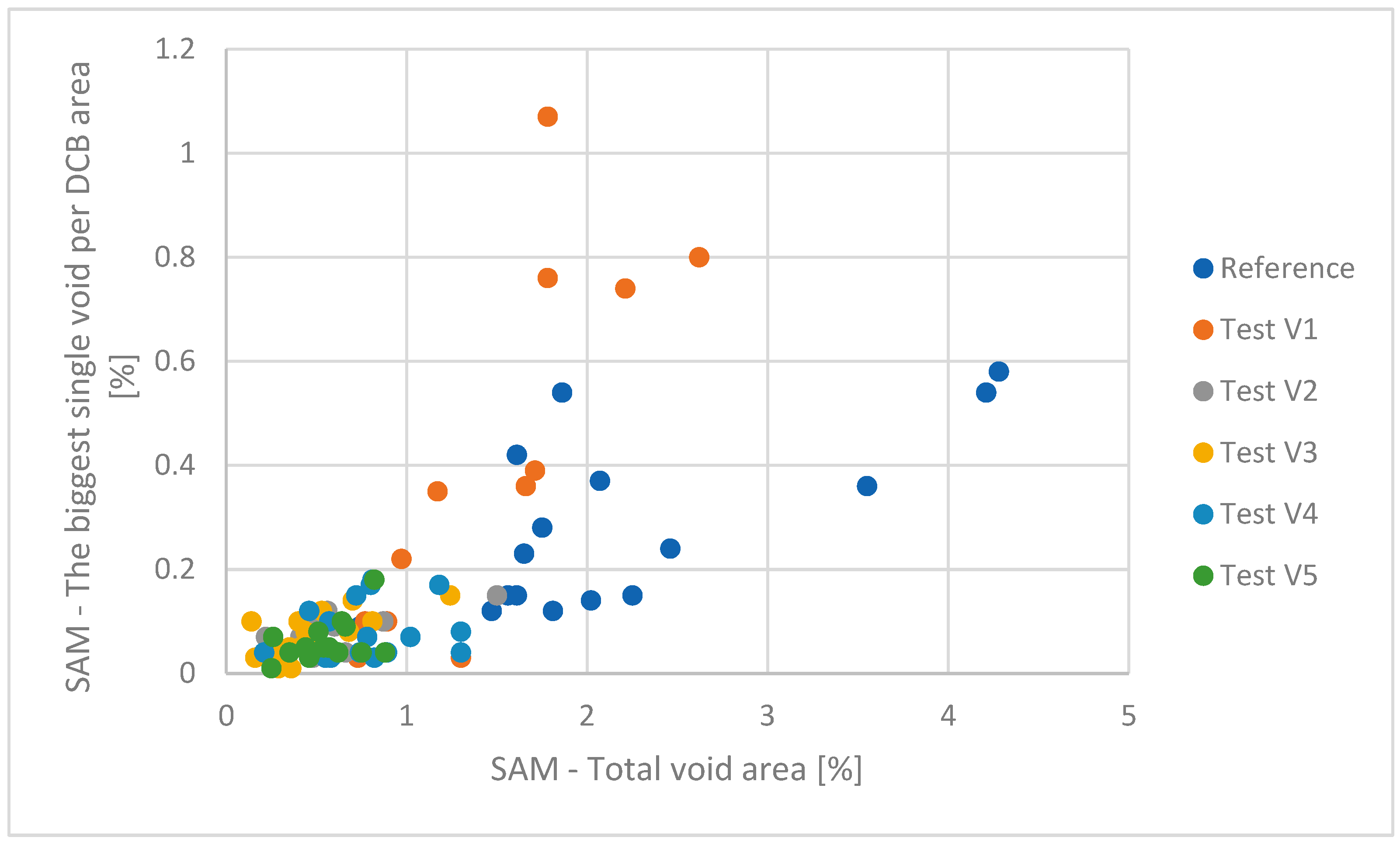
The reference group, with a formic acid exposure of 212 s, serves as the baseline, showing an average void area of 2.18%, a minimum void area of 0.74%, and a maximum void area of 4.28%. The largest single void area per DCB was recorded at 0.58%. These values represent 100% in terms of void presence, serving as the standard for comparison (
Figure 11 and
Figure 12).
Test group 1, with an extended formic acid presence of 281 s, showed a substantial improvement in void reduction. The average void area decreased to 1.21%, marking an 80% improvement over the reference group. The maximum void area decreased to 2.62%, a 63% improvement, while the largest single void area increased slightly to 1.07%, indicating a 54% improvement. The formic acid exposure time increased by 33% compared to the reference group.
In test group 2, with a formic acid presence of 401 s, the average void area further decreased to 0.53%, showing a remarkable 311% improvement. The maximum void area was reduced to 1.5%, a 185% improvement, and the largest single void area dropped to 0.15%, a 287% improvement. The formic acid exposure time increased by 89%, demonstrating the significant impact of prolonged exposure.
Test group 3 continued this trend, with a formic acid presence of 420 s, achieving an average void area of 0.47%, a 364% improvement over the reference group. The maximum void area decreased to 1.24%, a 245% improvement, while the largest single void area remained at 0.15%, a 287% improvement. The formic acid exposure time increased by 98%.
Test group 4, with a formic acid duration of 450 s, maintained low void areas, with an average void area of 0.8%, a 173% improvement. The maximum void area was 1.3%, a 229% improvement, and the largest single void area was 0.18%, a 222% improvement. The formic acid exposure time increased by 112%.
Finally, test group 5, with the longest formic acid presence of 608 s, showed an average void area of 0.55%, a 296% improvement. The maximum void area was reduced to 0.88%, representing a 386% improvement, and the largest single void area was 0.18%, thus representing a 222% improvement. The formic acid exposure time increased by 187%.
Test program descriptions are as follows:
Reference soldering program: Soldering program used in the previous experiment; first chamber cleaning in the HCOOH atmosphere for 60 s; temperature during HCOOH cleaning about 215 °C.
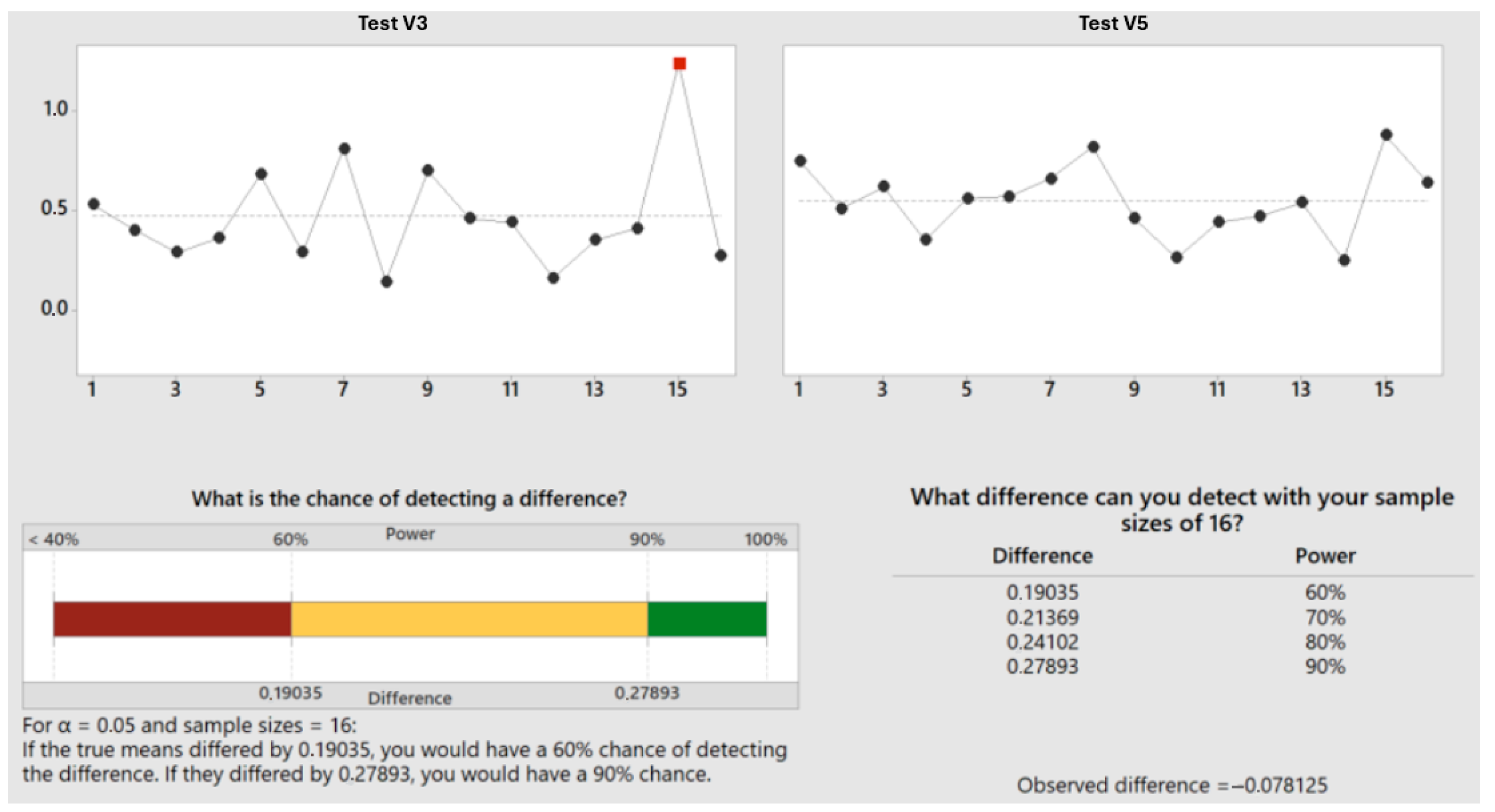
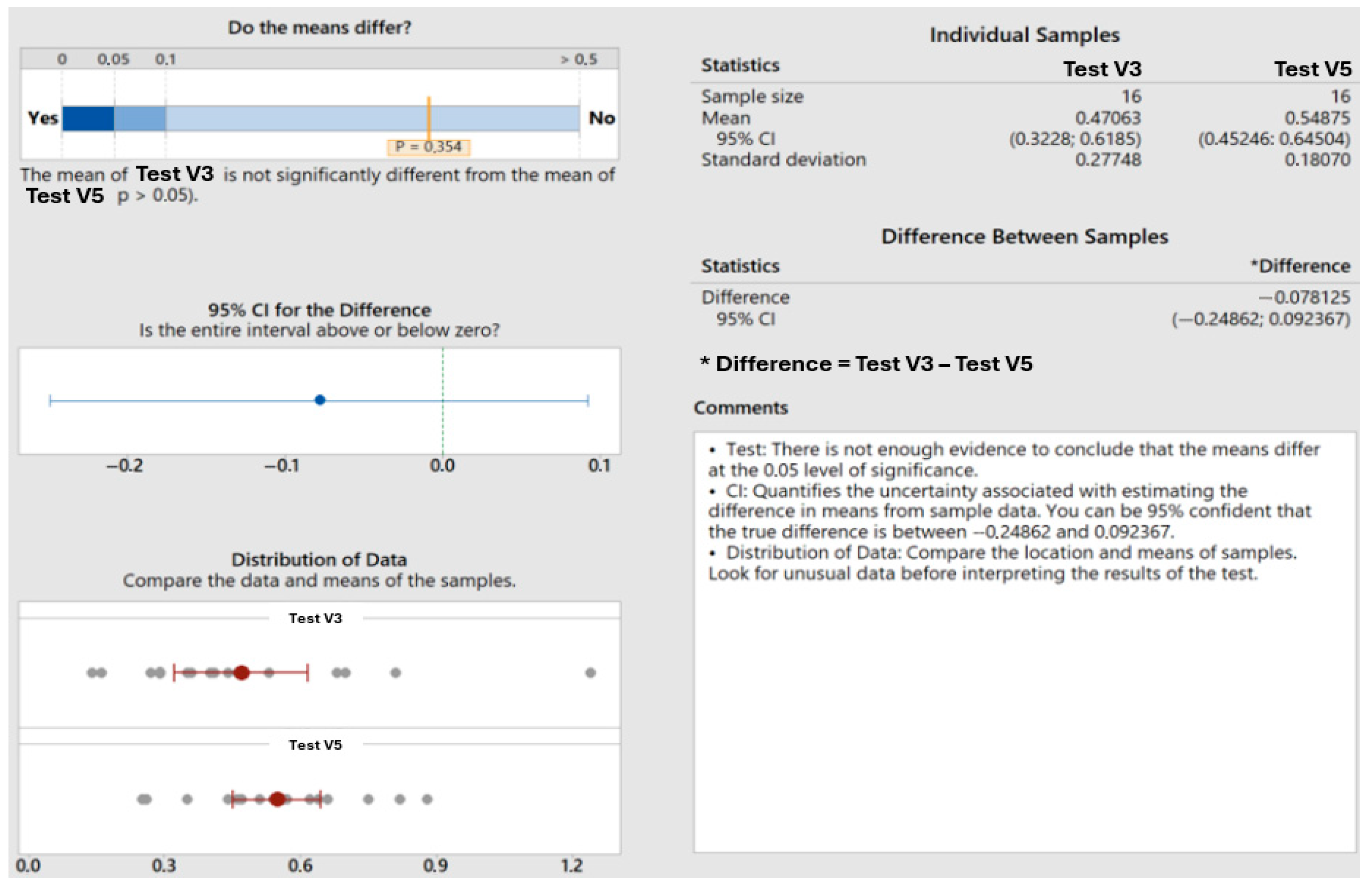
Test V1: Increased temperature in the first chamber during HCOOH cleaning, equal to the increase in activation energy of a reaction between formic acid and metal oxides; temperature measured on modules should be below the SnSb5 solid’s temperature, which is 235 °C; dwell time after HCOOH insertion was 120 s; the second chamber process was without changes.
Test V2: First chamber: dwell time after HCOOH insertion was 120 s; second chamber: after process start, there is a mixture of HCOOH from the first chamber and N2 from the second chamber; the first step is to create soft evacuation, flooding with HCOOH up to 30 L/min; after reaching final pressure 90 s dwell time for oxide reduction; temperature measured on modules should be below 220 °C; then evacuate to 5 mbar, flood with N2 to 100 mbar, and then perform the standard steps of the base program.
Test V3: First chamber dwell time after HCOOH insertion was 120 s; second chamber: after process start, in the chamber, there is a mixture of HCOOH from the first chamber and N2 from the second chamber; first step is the soft evacuation (longer flooding and more fresh HCOOH compared to version 2), flooding with HCOOH up to 30 L/min; after reaching pressure, 90 s is the dwell time for oxide reduction; temperature measured on modules should be below 220 °C as well; evacuate to 5 mbar, flood with N2 to 100 mbar, and then perform the standard steps of the base program.
Test V4: First chamber: dwell time after HCOOH insertion was 240 s; second chamber: without changes.
Test V5: First chamber: HCOOH lower flooding with 60 s dwell time; the idea of using a lower flow rate is the intention to possibly increase HCOOH concentration in the carrier gas; the longer flooding time is also the reaction time; second chamber: evacuate to 5 mbar, HCOOH flood with the slow flow rate up to 15 L/min, evacuate to 5 mbar, flood with N2 to 100 mbar, then perform the standard steps of the base program.
Overall, the results clearly indicate that increasing the duration of formic acid presence significantly enhances void reduction in soldered units (
Figure 13). This improvement is likely due to more effective chemical reactions between formic acid and metal oxides, leading to the better cleaning and preparation of surfaces for soldering. This data underscores the importance of optimizing formic acid exposure time to achieve high-quality solder joints with minimal void presence, and also highlights the substantial benefits of prolonged exposure in improving soldering outcomes.
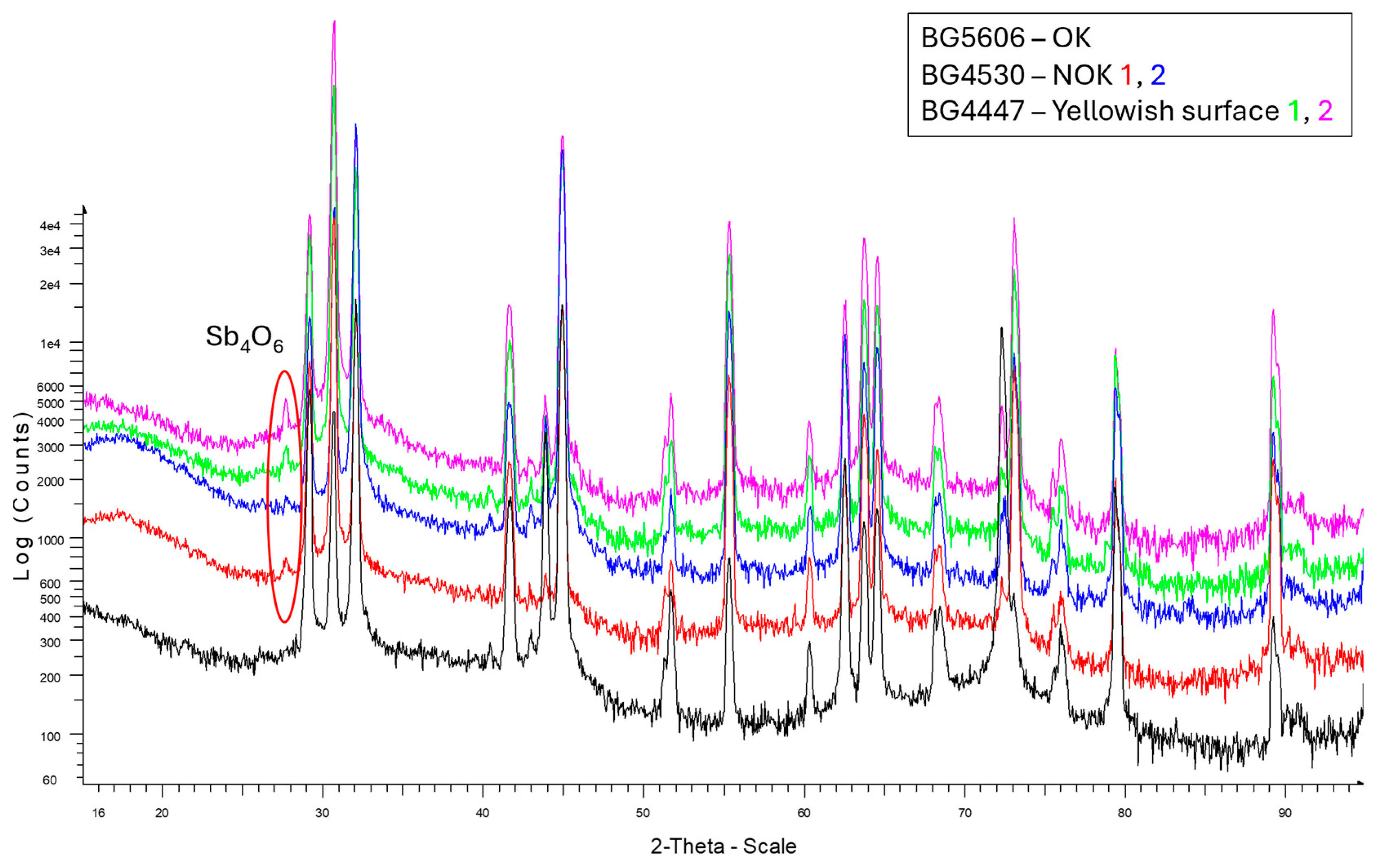
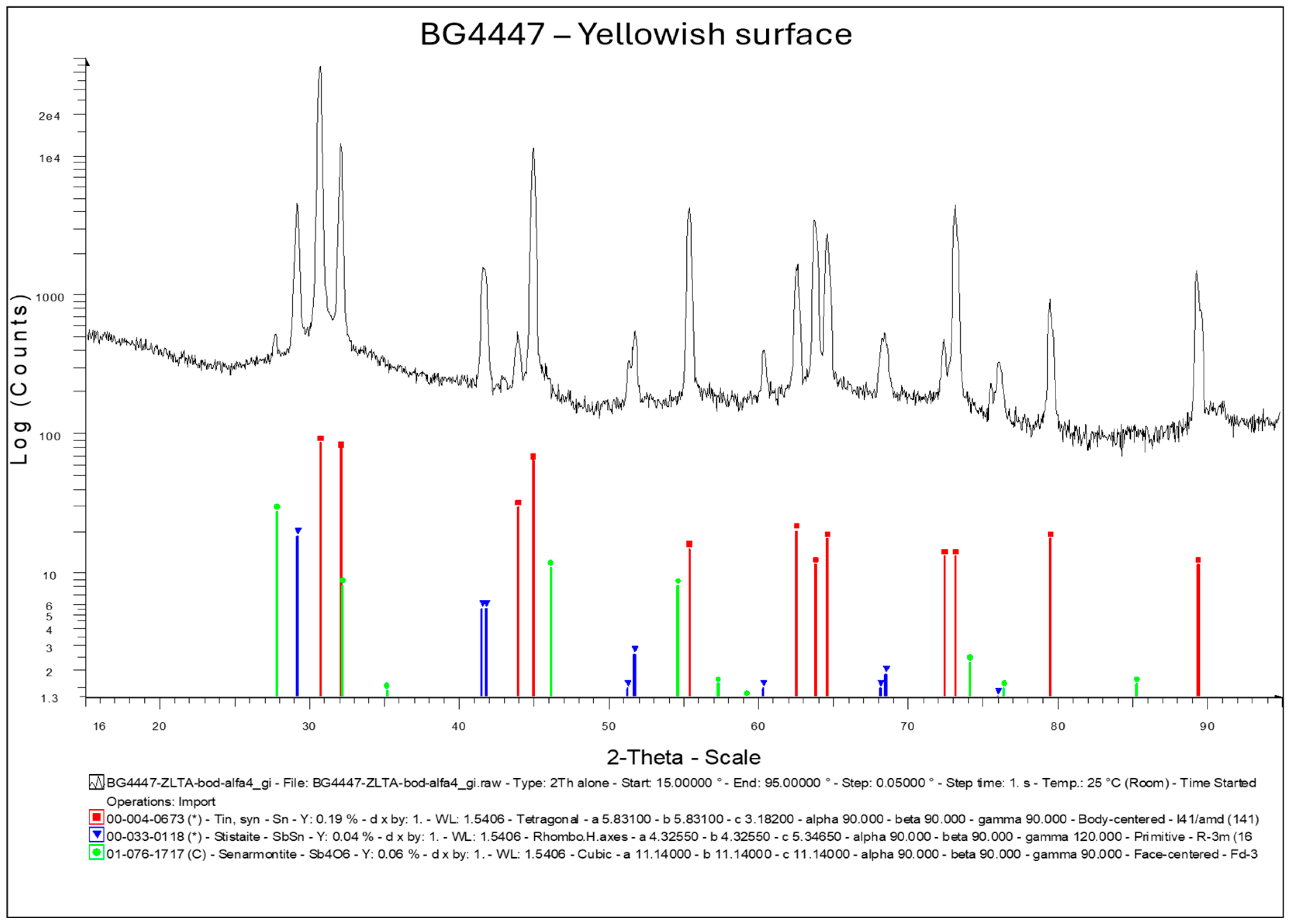
Highly flexible diffractometer enabled us to perform various types of X-ray diffraction analysis and reflectivity measurements of thin films with thicknesses ranging from micrometers down to a few nanometers. A diffractometer, Bruker D8 DISCOVER, equipped with a rotating Cu anode operating at 12 kW, was used (standard θ/2θ and Grazing incidence X-ray diffraction) for soldering preform analysis to identify the impurities on the surface that were removed by formic acid in the soldering process. For analysis, we chose a solder preform with yellowish surface discoloration that showed poor wetting and a silver preform surface that showed satisfactory wetting (
Figure 5). Results from the X-ray diffraction analysis are shown on
Figure 14. On the preform with a yellowish surface, we observed antimonoxyde Sb
4O
6. The thickness of the oxide was not measured.


