Article

The Study of the Synthesis of SiC by the Carbonization of Si(111) Substrates: The Role of Native Silicon Oxide

1
“Acad. E. Djakov” Institute of Electronics, Bulgarian Academy of Sciences, 72 Tzarigradsko Chaussee Blvd., 1784 Sofia, Bulgaria
2
“G. Nadjakov” Institute of Solid State Physics, Bulgarian Academy of Sciences, 72 Tzarigradsko Chaussee Blvd., 1784 Sofia, Bulgaria
3
National Centre of Excellence Mechatronics and Clean Technologies, Bulgarian Academy of Sciences, 8 Kliment Ohridski Blvd., Blk. 8, 1756 Sofia, Bulgaria
4
Institute of General and Inorganic Chemistry, Bulgarian Academy of Sciences, “Acad. Georgi Bonchev” Str. bld.11, 1113 Sofia, Bulgaria
5
Institute of Physical Chemistry “Rostislaw Kaishev”, Bulgarian Academy of Sciences, “Acad. Georgi Bonchev” Str. bld.11, 1113 Sofia, Bulgaria
6
Institute of Optical Materials and Technologies “Acad. Jordan Malinowski”, Bulgarian Academy of Sciences, 109, Acad. G. Bontchev Str., 1113 Sofia, Bulgaria
7
Faculty of Physics, Sofia University “St. Kliment Ohridski”, 5 James Bourchier Blvd., 1164 Sofia, Bulgaria
*
Author to whom correspondence should be addressed.
Appl. Sci. 2025, 15(13), 7078; https://doi.org/10.3390/app15137078
Submission received: 3 May 2025 / Revised: 12 June 2025 / Accepted: 20 June 2025 / Published: 23 June 2025
(This article belongs to the Section Surface Sciences and Technology)

Abstract

Featured Application

Our experimental studies show that the synthesized SiC thin films with a complex composition do not contain cracks and/or voids and can be used as an intermediate layer for further synthesis of thicker single-crystalline SiC layers for direct application in electronic element production and technology.

Abstract

We present the results of silicon carbide (SiC) thin film synthesis on Si(111) substrates using chemical vapor deposition by decomposing CH4 in H2 at 1135 °C. The experiments were conducted in an Oxford Nanofab Plasmalab System 100 for carbon phase deposition times of 3, 5, 20, 60, and 90 min on Si(111) with or without native oxide, following established protocols. Our studies show that either predominantly crystalline SiC or a mixture of SiC and Si–O/Si–O–C glass forms on Si substrates significantly doped with carbon and oxygen, depending on the presence or absence of native oxide. The thickness of the SiC film ranges from approximately 5–6 nm for films synthesized in 3 min to over 15 nm for those synthesized in 90 min, while the size of the crystal grains varies from a few to 110 nm depending on the synthesis duration. The findings suggest that the complex composition of the thin films and the region beneath them can more effectively compensate for the differences in lattice parameters and thermal expansion coefficients between the SiC film and the Si substrate; thus, this method is promising for depositing intermediate thin films of SiC on Si substrates.

1. Introduction

SiC is a wide-bandgap binary semiconductor that has been extensively studied since the first method for reproducible synthesis was patented more than a hundred years ago [1]. Furthermore, SiC applications are proliferating, with the industrial production of single-crystal ingots being realized mainly by three methods: Physical Vapor Deposition (PVD), chemical vapor deposition (CVD), and high-temperature solutions [2].
It is well known that SiC crystallizes in three stable modifications: cubic, hexagonal, and rhombohedral. The coordination polyhedron is a Si-centered tetrahedron with C atoms at its vertices. The cubic structure of SiC is of the zinc-blende type that can be described as a series of double Si and C atomic layers along the (111) planes arranged one above the other along the [111] direction, often abbreviated as …cCaAbBcC…, where a, b, and c represent layers of Si atoms in one orientation and A, B, and C represent layers of C atoms in an orientation rotated by 60 degrees.
The structure of SiC and the strong Si–C bonds predetermine the formation of various polytypes, with more than 250 different polytypes reported so far [3]. The SiC polytypes represent structural defects associated with a change in the arrangement of the Si–C double layers, thus often changing the symmetry of the crystal lattice and its parameters. Their classification and description have been summarized in various publications (e.g., [4]), with 3C–SiC meaning SiC with a cubic structure, while 2H–SiC is a polytype with an entirely hexagonal structure. The 3C–SiC polytype is thermodynamically stable, i.e., it is expected to be reproducibly synthesized at temperatures lower than 1500 °C. For a long time, the heteroepitaxial deposition of high-quality 3C–SiC layers on Si single-crystalline substrates as an industrial product with highly reproducible quality has been considered difficult to achieve because the cell parameters of 3C–SiC and Si, as well as their thermal expansion coefficients, are significantly different. Nishino et al. [5] have demonstrated for the first time a way to circumvent these problems with the so-called two-step method consisting of the deposition of an intermediate carbon layer at high temperature above 1300 °C by pyrolysis of propane in hydrogen and the subsequent deposition of a SiC layer synthesized from a hydrocarbon precursor and silane in a hydrogen flow at similar temperatures. The intermediate layer formed in the first stage compensates for the incommensurability of the lattices of the two materials. This layer allows for the synthesis of high-quality SiC in the second stage of the process. Later on, Severino et al. [6] have investigated the deposition of high-quality SiC films on 6′ Si substrates with orientations (001), (011), or (111) in a four-step process in which, compared to the original one by Nishino et al. [5], two initial steps have been added, namely annealing in high vacuum of 10−5 Torr and temperatures of about 500–600 °C for several hours and the deposition of SiC by carbonization in a CVD process at about 1120 °C and increasing the temperature to the working temperature of about 1350 °C for the synthesis of SiC from trichlorosilane and ethylene. We note that the intermediate film synthesis of nanocrystalline SiC usually occurs at temperatures above 1200 °C [5,6].
In the last decade, several papers [7,8,9] have been published discussing the direct carbonization of Si substrates using carbon oxides based on theoretical and experimental studies of the pathways for these reactions, including studies of some intermediate products. It should be noted that Kukshkin et al. [7,9,10] studied the problems of the carbonization of Si(111) by CO and concluded that carbon oxide can interact with silicon, forming SiC on the surface, and managed to develop the method to a practical application, namely the synthesis of intermediate SiC nanofilm on Si substrates for the further deposition of AlInGaN heterostructures for LED devices [11].
It should be noted that researchers generally assume that the natural SiO2 covering Si substrates is extremely harmful and is chemically eliminated according to established protocols prior to or during the pretreatment of the substrates at high temperature, especially when chlorine gas is used. To prevent the formation of small amounts of oxides, some researchers deposit a thin film of carbon before the carbonization process [6]. The deposition of only an intermediate film of SiC was thoroughly analyzed in two publications [12,13], where the thin films were characterized only by scanning electron microscopy (SEM) and transmission electron microscopy (TEM), and due to the complexity of these methods, the characterization results appear incomplete.
Over the past few years, research has been conducted in two main directions: the development of the CVD methods for the synthesis of SiC coatings for specific purposes and the synthesis of SiC in low-dimensional allotropic forms—1D or 2D by CVD methods. For example, Sato et al. [14], for the synthesis of SiC on graphite, use only polysilaethylene instead of two different gases providing Si and C in the reaction space, but the reaction is carried out at a high temperature (1200–1500) °C, while Steiner et al. [15] propose synthesis at temperatures around 1120 °C (i.e., compatible with silicon technologies for microelectronics) from silane and propane on different substrates: Al2O3, Si/SiO2, etc. Different studies are carried out also for obtaining gas-tight SiC coatings to protect carbon fibers/nanotubes from oxidation, ceramic parts from harmful gas effects, etc.—see Refs. [16,17]. In principle, these methods are associated with reactions at very high temperatures—above (1400–1800) °C—with the latter method [17], for example, being associated with thermal evaporation of Si from a crucible at a temperature above that of Si melting, with C being provided by the reduction of hydrocarbon gas (e.g., methane). Another major area of interest for researchers in the past few years is the synthesis of low-dimensional forms of SiC—e.g., 1D (see e.g., [18,19,20] and 2D/quasi 2D (see e.g., [21])).
In a recent study, we successfully simulated the synthesis of SiC with methane on a Si(111) substrate at a temperature of 1423 K [22]. The investigation of the mechanism included all intermediate products and transition states. It was concluded that native oxide does not suppress the process and that the carbon atoms are incorporated in the Si wafer only after the complete hydrogen loss. At high temperatures, the crystal surface is in continuous reconstruction, and no substitution reaction is necessary for carbon incorporation in the silicon structure. Two mechanisms of native oxide reduction were also proposed.
In this work, we experimentally investigate the formation of the intermediate SiC thin films by the direct carbonization of Si substrates at about (1130–1140) °C, i.e., at temperatures at which standard quartz equipment can be used, focusing on the influence of the native oxide on the results.

2. Materials and Methods

We used one-sided polished Si(111) wafers (Wacker Chemie, Munich, Germany) with a diameter of 3 inches. The precursors for all processes were N2 (99.999%), H2 (99.999%), Ar (99.9999%), and CH4 (99.9995%) (Linde Gas Bulgaria, Sofia, Bulgaria).
The carbonization processes were performed via the CVD method in an Oxford Nanofab Plasmalab System 100 (Oxford instruments, Abingdon, UK) apparatus. All experiments at defined process parameters were conducted first with substrates with native oxide and then with substrates with removed native oxide, following the established protocols (e.g., [23,24]). To verify the reproducibility of the CVD processes, the experiments were carried out at least two or three times with reproducible results. For the reduction of the native oxide in all experiments, the substrates were cleaned in Ar plasma at a temperature of 250 °C (Ar flow of 500 sccm, pressure of 3000 mTorr, power of 50 W, mid-frequency plasma at 13.56 MHz, and time of plasma etching of 10 min). Subsequently, all substrates were annealed in an H2 atmosphere (flow of 500 sccm, pressure of 200 mTorr) at a temperature of 1150 °C for 5 min before the processes of the direct carbonization of the Si surface.
All thermal processes were conducted in a vacuum of 200 mTorr (thermal annealing before the carbonization processes) or 300 mTorr (processes of heating, cooling, and carbonization). The heating process was carried out at a speed of about 600 °C/h with a break of 10 min at 250 °C for etching in Ar plasma in all cases. The carbonization processes were carried out by a thermally stimulated CVD process of methane (CH4) decomposition at about 1130–1140 °C and pressure of 300 mTorr in a gas mixture of H2 (500 sccm) and CH4 (10 sccm). The duration of the carbonization processes in the different experiments was 3, 5, 20, 60, and 90 min. After the carbonization, the reactor was allowed to cool naturally for about 15–18 h in a weak flow of Ar and H2 gases. The experimental procedures for the carbonization processes are also presented graphically (Figure S1).
The thickness of the films was measured with a TALYSTEP (Rank Taylor Hobson, Leicester, UK) profilometer and an atomic force microscopy (AFM), and the samples were scratched with an Ultra-High Strength Steel (UHSS) blade to access the thin film/substrate interface and to collect material for the TEM sample preparation. The AFM measurements were performed on the MFP-3D Origin (Oxford instruments, Asylum Research, Santa Barbara, United States Abingdon, UK) apparatus. The images were taken in a tapping mode. The measurements were carried out at steps of 20 µm at scanning rates per line of 1.0 Hz and image resolution of 256 × 256 points. Silicon probes with a cantilever length of 160 µm and an Al reflective coating on the backside (AC160TS-R3, Olympus, Hamburg, Germany) were used in the experiments. These probes had a nominal resonance frequency of the cantilever of 300 kHz and a typical force constant of 26 N/m. The nominal tip radius for these probes was 7 nm. Before the analysis, the images were flattened, and no further processing was performed. The image analysis was performed using Gwyddion 2.56. The ellipsometry measurements were performed using a Woollam M2000D (J.A. Woolam Co Inc., Lincoln, NE, USA) rotating compensator spectroscopic ellipsometer with a wavelength range from 193 to 1000 nm. The data acquisition and modeling software was CompleteEASE v.5.19 (J.A. Woollam Co., Inc.).
SEM investigations were conducted using a LYRA TESCAN (SEM) (TESCAN GROUP a.s., Brno, Czech Republic) microscope in secondary electron image and backscattered electron image (SEI and BEI, respectively). Elemental analysis was performed by energy-dispersive X-ray analysis (EDX) at a Brucker QUANTAX 200 Spectrometer (Brucker Co., Elk Grove Village, IL, USA) unit. Optical profilometry measurements were performed by Zeta™-20 3D Optical Profiler (Zeta Instruments, KLA Instruments Group, Milpitas, CA, USA).
X-ray Photoelectron spectroscopy (XPS) was used to obtain the spectra with unmonochromatized Al Kα (1486.6 eV) radiation in a VG ESCALAB MK II (Thermo Scientific, Waltham, MA, USA) electron spectrometer under a base pressure of 1 × 10⁻⁸ Pa. The spectrometer resolution was calculated from the Ag 3d5/2 line with analyzer transmission energy of 20 eV. The line full width at half maximum (FWHM) was 1 eV. The spectrometer was calibrated against the Au 4f7/2 line (84.0 eV), and the sample charging was estimated from C 1s (285 eV) spectra from natural hydrocarbon contaminations on the surface. The accuracy of the binding energy determination was 0.2 eV. The photoelectron spectra of C 1s, O 1s, Si 2p, N 1s, and a small amount of detected contaminations, such as F 1s and Cu 2p, were recorded and corrected by subtracting a Shirley-type background and quantified using the peak area and Scofield’s photoionization cross-sections. The peak fitting was conducted using XPSPEAK4.1 software. The in-depth elemental composition analysis of the thin films was obtained by two different techniques—by sputtering with an Ar beam and by glow discharge optical emission spectroscopy (GDOES) using a GDA 750 HR GDOES (Spectruma Analytik GmbH, Hof, Germany) spectrometer.
X-ray diffraction (XRD) as well as Grazing Incidence XRD (GIXRD) measurements were performed using PANalytical Empyrean apparatus in different geometries (φ, (θ−2θ), and (ω−2θ) scans). The Raman spectroscopy studies were accomplished with a micro-Raman HORIBA Jobin Yvon (HORIBA Jobin Yvon, Longjumeau, France) LabRAM HR 800 spectrometer (excitation with a He/Ne (633 nm) laser). The laser beam with power of 0.5 mW was focused on a spot of about 1 μm in diameter on the studied surfaces, the spectral resolution being about 1 cm−1 or better. The TEM in high-resolution (HR TEM) mode and selected area electron diffraction (SAED) were carried out on an HR STEM JEOL JEM 2100 (Jeol Ltd., Akishima, Tokyo, Japan) microscope at 200 kV accelerating voltage.

3. Results

The experimental conditions of the various experiments and the thicknesses of the obtained films are shown in Table 1 as well as in Figure S1. The samples obtained under different conditions will be denoted with a capital letter O (those with natural oxide) or C (those with a deeply cleaned surface) and a numerical designation 3, 5, 20, 60, or 90, depending on the duration in minutes of the carbonization process.
To measure the thickness of the thin films using AFM and the Talystep profilometer, the films were marked by scratching with a hardened steel needle. However, the resulting scratches lack a clearly defined flat transition between the layer and the substrate, significantly complicating the accurate determination of scratch depth. Additionally, localized areas (approximately 3 × 3 mm2) were ablated using laser radiation. For this purpose, the fourth harmonic (λ = 266 nm) of a nanosecond Nd:YAG laser system (fundamental wavelength λ = 1064 nm, frequency = 10 Hz, pulse duration = 15 ns, energy = 14 J/cm2) was applied for 2–5 s, depending on the carbonization time (3–90 min). Studies conducted using both methods confirmed the impossibility of selectively removing only the thin film down to the thin film/Si-substrate interface. We attribute the failure of mechanical cleavage to the excellent adhesion of the thin films to the substrates. Similarly, the challenges encountered in laser ablation can be linked to the significant surface roughness of the ablated area. Difficulties in phase visualization in electron microscopy arise due to the close atomic numbers of Si, O, and C as well as those of SiC and Si–O–C glasses with variable composition. Given these limitations, we consider the results obtained from the indicated measurements to be insufficiently reliable; therefore, they are not presented here.
The thickness of the synthesized thin films C3, C5, O3, and O5 was determined by ellipsometric measurements, and it is 12, 12, 13.5, and 15 nm, respectively. To maximize the precision of the fits, we used as input parameters the results of the XPS and GDOES studies on the composition of the films, and they were approximated with layers containing 4H–SiC and Si–C–O glass, assuming the absence of a discrete SiO(2−x) phase. The presumed change in the thin film composition in depth and the poorly defined interface make this approximation inapplicable to the ellipsometric analysis of films synthesized for 20 min or longer. In these cases, the thickness data for the samples C20, O20, C60, O60, C90, and O90 obtained by AFM, profilometry, and ellipsometry differ significantly, and for this reason, concrete values are not indicated.
The powder XRD patterns taken in (θ−2θ) scans of the synthesized films C3, C5, C60, C90, and O90 (Figure 1) show the formation of clearly structured crystallites of polycrystalline SiC, especially in the longer experiments C90 and O90. The XRD patterns of C90 and O90 are indexed in the hexagonal cell of the 36H polytype of SiC [25], which possesses trigonal symmetry (space group (SG) #156 and cell parameters a0 = 3.0730 Å, c0 = 90.6500 Å). Furthermore, the strongest reflections (Figure 1 and Figure S2c) can be assigned to reflections of d(00-30), d(00-32), d(00-36), d(00-39), and d(00-58), while the weak ones, denoted by w1 and w2, can be assigned to reflections of d(00-31) and d(00-36), respectively (Figure 1). Strong reflections are associated with distances between crystal planes of 3.0217 Å, 2.8328 Å, 2.3244 Å, and 1.5629 Å, while the weak ones are associated with 2.9242 Å and 2.5181 Å, respectively. The observed inconformity in their intensity ratios and their distinct broadening could be attributed to the presence of a second phase of other SiC polytypes, deviations in the arrangement of the layers in the polytypes, and the small size of the crystallites in the layer. The careful analysis of the XRD patterns of C90 and O90 shows that slightly shifted satellite peaks with different intensities are superimposed on the peaks denoted by 1 and 2 (Figure S2). This indicates that the samples are probably two-phased, with the 96R polytype of SiC with rhombohedral symmetry (SG #160 R3m and cell parameters a0 = 3.0800 Å, c0 = 241.9000 Å [26]) being the most likely candidate for a second crystalline phase—see Figure S2. These reflections are associated with distances between crystal planes of d(00-81) = 2.9864 Å and d(00-96) = 2.5198 Å, respectively. The reflection at about 2θ = 35.1° cannot be associated with any of the structures mentioned so far but is very close to the reflection from d(001) = 2.333 Å of 19H–SiC (which possess trigonal symmetry (SG #156 P 3m1 and cell parameters a0 = 3.0730 Å, c0 = 47.7530 Å) [27].
It is also obvious that during the carbonization of C60 (blue trace in Figure 1), the crystallites of the thin films are in the nanoscale range, as the I-denoted reflection arising from the (111) planes of cubic 3C–SiC (cubic symmetry (SG #216 F-43m and cell parameter a0 = 3.3480 Å) [28] becomes weak and very broad. There is no trace of crystalline phases in the diffraction patterns obtained from samples C3, O3, C5, and O5 (Figure 1).
To clarify the structural quality of the thin films from the C60 samples, GIXRD was used in φ and (ω−2θ) scans. The value of the optimal grazing angle (ω) was determined by (ω−2θ) scans to be ω = 0.25°, which corresponds to the maximum intensity of the d(111) peak (Figure 2a). We used φ scans in the range φ = (0–180)° regarding d(111) = 2.5103 Å of 3C–SiC at 2θ = 37.75° [28] (Figure 2a) and to determine the most preferred orientation for further GIXRD studies. A change in the number of the counts per second (cps) between 2 and 3 times compared to the optimal orientation at φopt was found; with deviations of 100 relative to φopt, the signal decreases by 15–25% (Figure 2b). Furthermore, the GIXRD patterns in (ω−2θ) scans taken at φopt as well as (φopt − 10°) and (φopt + 10°) and ω = 0.25°, presented in Figure 2c, show the real change of the maximum intensity of the d(111) peak [28] at the corresponding conditions.
The measured XRD and GIXRD patterns (Figure 1 and Figure 2) allow for the calculation of the grain size of the crystal grains in samples C60, C90, and O90 according to the Scherrer equation [29] and a more complete characterization of the films deposited after longer carbonization processes. The calculated values in the (θ–2θ) scans (Figure 1) are about 7 nm for C60 and about 110 nm for the C90 and O90 samples. In these calculations, the peak of d(00-39) was used because no peaks of the second phase are observed in its vicinity (Figure S2a–e). The GIXRD patterns measured in (ω–2θ) scans (Figure 2) allow for the derivation of the grain size for C60 of about 6 nm (Figure S2f).
XPS was used to study the as-prepared SiC films on Si(111) substrates. This technique, as is well known, can be used in nondestructive and destructive modes. We applied XPS in the nondestructive mode to detect the surface concentrations of the constituent elements and the chemical bonds among them in the deposited thin film. The evaluated surface concentrations are given in Table S1.
The deconvoluted C 1s and Si 2p XPS spectra of the studied samples are presented in Figure 3a–d, Figures S3a–d and S4a–d. In the spectral series of the C 1s, core level peaks of the samples four main contributions were identified and attributed to C–Si (carbon in Si carbide and Si oxicarbide), C–C (carbon), and C–O (carbon bonded to O, C–O, or C=O) at about 283.2 eV, 285.0 eV, 286–287 eV, and above 288 eV binding energies, respectively [30]. The Si 2p XPS spectra were also resolved as the sums of several components. Four main components were observed in the Si 2p spectra: Si–Si (elemental silicon due to unreacted silicon or to the silicon substrate), Si–C (silicon carbide), Si–O–C (silicon oxicarbide), and Si–O (silicon oxide), located at 99.8, 100.2, 101.7, and 103.8 eV binding energies, respectively. These values agree well with those for the pure stoichiometric phases Si, SiC, and SiO2 [31].
The study of the depth-dependent elemental distribution is of utmost importance for the SiC films synthesized by direct carbonization on Si(111) substrates. In our case, we use a depth resolution better than 3 nm, and the information depth of a 45° exit angle measurement is around this size (1–3 nm). For these studies, samples O3 and O5 were preferred since in the samples with non-removed native oxide, the change in the ratio of SiO2 and Si–O–C can be traced, these films are thin, and the effects of a strong change in surface roughness are the weakest, as the processing time is the shortest. The depth profiles were obtained by sputtering with an Ar plasma beam for a fixed duration, and the changes in the surface composition and chemical state of the elements of interest (C, O, and Si) were monitored. The corresponding C 1s, Si 2p, and O 1s specific peaks were examined to derive the relative abundance changes, while the peak shifts in the binding energies indicate changing bound states as a function of depth.
The normalized in-depth distributions are presented in Figure 4a–f. For each sputtering time, the recorded C 1s, O 1s, and Si 2p XPS spectra were fitted, and as a result of the fitting, the similar evolution of depth profiles was drawn by components. At each sputtering, the recorded C 1s, O 1s, and Si 2p photoelectron spectra were fitted, and as a result of the fitting, the similar evolution of depth profiles was drawn out by components. It should be noted here that prolonged sputtering will lead to a significant increase in the information depth and to a decrease in resolution due to surface roughening. In a compound material such as SiC, the silicon atoms are more rapidly removed than the carbon atoms. Thus, the Si/C ratio may be observed close to 1/3 instead of the expected 1/1 [32]. A significant result of these studies is the established diffusion of oxygen and carbon atoms as silicon oxide with variable composition and as Si−O−C ensembles in the regions near the surface of Si substrates.
The in-depth distribution of Si, C, and O in the films was investigated via the GDOES method using the Spectrum Analytic GDA 750 HR. The depth profiles were measured in RF mode (constant voltage, regulated pressure) with the optimized parameters: Si–C (800 V, 3 hPa). After an evacuation period of 30 s, the sample surface was flushed with the analytical gas (Ar 99.999%) for 30 s. The results for some of the characterized samples are shown in Figure 5a,b and Figure S5a–d. Here, we must point out the following:
-
Due to the removal of material from the thin films by a directed plasma flow, a significant predominance of Si atoms sputtered from the SiC as a part from the thin film is expected compared to those of carbon.
-
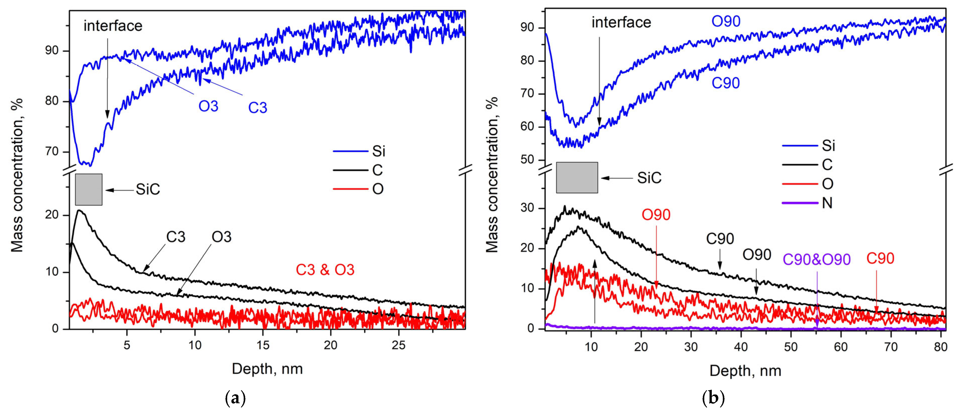
The elemental analysis in the GDOES method refers to the atoms sputtered from the sample surface, while in the depth-dependent concentration profiles, the solid phase (unsputtered) of the samples is analyzed, and in this sense, the two methods, when analyzing identical samples, give a picture as close as possible to the real one.
Figure 5. (a) The GDOES study of C3 and O3 samples: the mass concentration of Si is drawn by blue traces, while those of C and O are drawn by black and red traces, respectively. (b) The GDOES study of C90 and O90 samples: the mass concentration of Si is drawn by blue traces, while those of C, O, and N are drawn by black, red, and violet traces, respectively.
Applsci 15 07078 g005
The mass concentration distribution of Si, C, and O in the depth of the thin films clearly shows that there is no clearly defined interface between the thin film and the substrate. However, we can assume that the thin film begins at the sample surface and extends approximately to the point where the carbon concentration decreases by 2–4% from its maximum, while the silicon concentration increases correspondingly. Based on this, the approximate thickness of the thin films is 4–5 nm for samples C3 and O3, 5–6 nm for C5 and O5, around 7 nm for C20 and O20, 9–10 nm for C60 and O60, and 12–13 nm for C90 and O90. Additionally, in the samples from which the native oxide has not been properly removed, (i) the concentration of the main components varies within large limits at different points on the surface of the thin films as shown in Figure 4a for sample O60; (ii) in the region in which there is a close to constant distribution of Si and C, the concentration of SiC is significantly lower than its corresponding value for the samples with properly removed native oxide.
The samples for TEM examinations were prepared by mechanically scratching the surface of the samples with a UHSS blade. A suspension in double-distilled water was prepared from the separated flakes, and the resulting colloid was collected by dropping and drying the drops on a FORMVAR-covered copper mesh.
The results of the TEM-examined samples (Figure 6a,d, Figure 7a,c, Figure 8a,b, Figure 9a–c, Figures S6a,b and S7a,b) show that the thin films consist of mixed nanocrystalline and amorphous masses in different ratios, and in general, with increasing synthesis time, well-ordered nanocrystals predominate. This effect is most clearly visible in the HRTEM images taken from the samples synthesized for 90 min (Figure 9a,b and Figure S7a,b).
Another important observation is that both SAED and HRTEM images of thin films synthesized on substrates with a properly removed native oxide can be indexed in ordered phase 36H–SiC only [25]. All interplanar distances in the HRTEM images (Figure 6c,d, Figure 8b, Figure 9c and Figure S6b) were also determined, and we found that they correspond to the indicated polytype of SiC, namely 36H–SiC [25]. The analysis of the SAED and HRTEM images taken from samples from which the native oxide was not properly removed (Figure 7b and Figure S6b) showed the presence of ordered phases based on SiO2—both crystalline SiO2 [33] and the complex compound Si(OCOCH3)4 [34].
The analysis of the synthesized thin films with TEM also shows certain trends:
(i)
The crystallite size in the thin films synthesized for 60 and 90 min is much larger than in the other samples.
(ii)
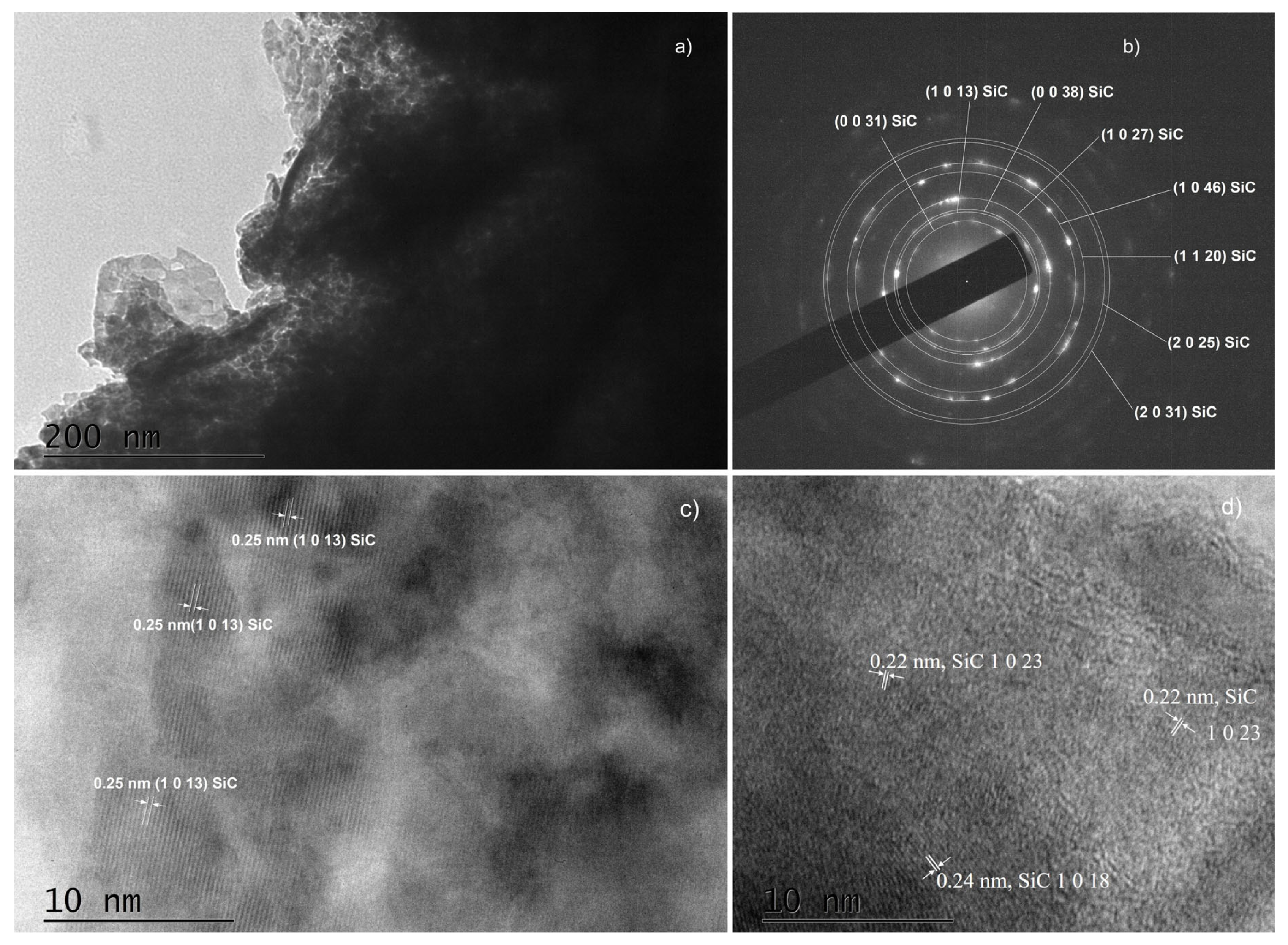
In the thin films synthesized for 90 min, there are a lot of areas in which a two-dimensional network of crystal planes is clearly distinguished, which indicates an enhanced crystalline ordering (Figure 9c and Figure S7b).
It is well known that the different polytypes of SiC have a clearly expressed and well-studied single-phonon Raman spectrum (100–1000) cm−1 [35]. Its overtones and combination bands also give a very pronounced spectrum in the interval (1300–1900) cm−1. The Raman spectrum of graphite, single- and multi-layer graphene, diamond-like phases, and amorphous carbon in its various modifications (amorphous carbon (aC), tetrahedral carbon (taC), etc.) also have a well-studied Raman spectrum, which can be used to identify these phases [36,37]. Therefore, all synthesized thin films were thoroughly studied via Raman spectroscopy. Figure S8 shows typical Raman spectra observed from the Si(111) substrate and a thin film from sample C90. As can be seen, the most prominent peaks of the two spectra coincide completely in terms of frequency/wavenumber, while their intensities are also approximately the same. The two spectra completely coincide in the region of the one-phonon spectrum of SiC (150–1000) cm−1 (Figure S8). The spectra of sample C90 do not differ from those of silicon in the region (1000–2100) cm−1. However, to identify any differences between the two spectra, we subtracted from the measured spectrum of C90 (red trace in Figure S8) that of Si(111) (black trace in Figure S8). No peaks can be distinguished in the resulting spectrum (inset of Figure S8). These results unambiguously confirm the absence of ordered phases of SiC or ordered or disordered carbon on the surface of the thin films or in their vicinity.

4. Discussion

The results presented above as well as those provided in the Supplementary Information show the following:
-
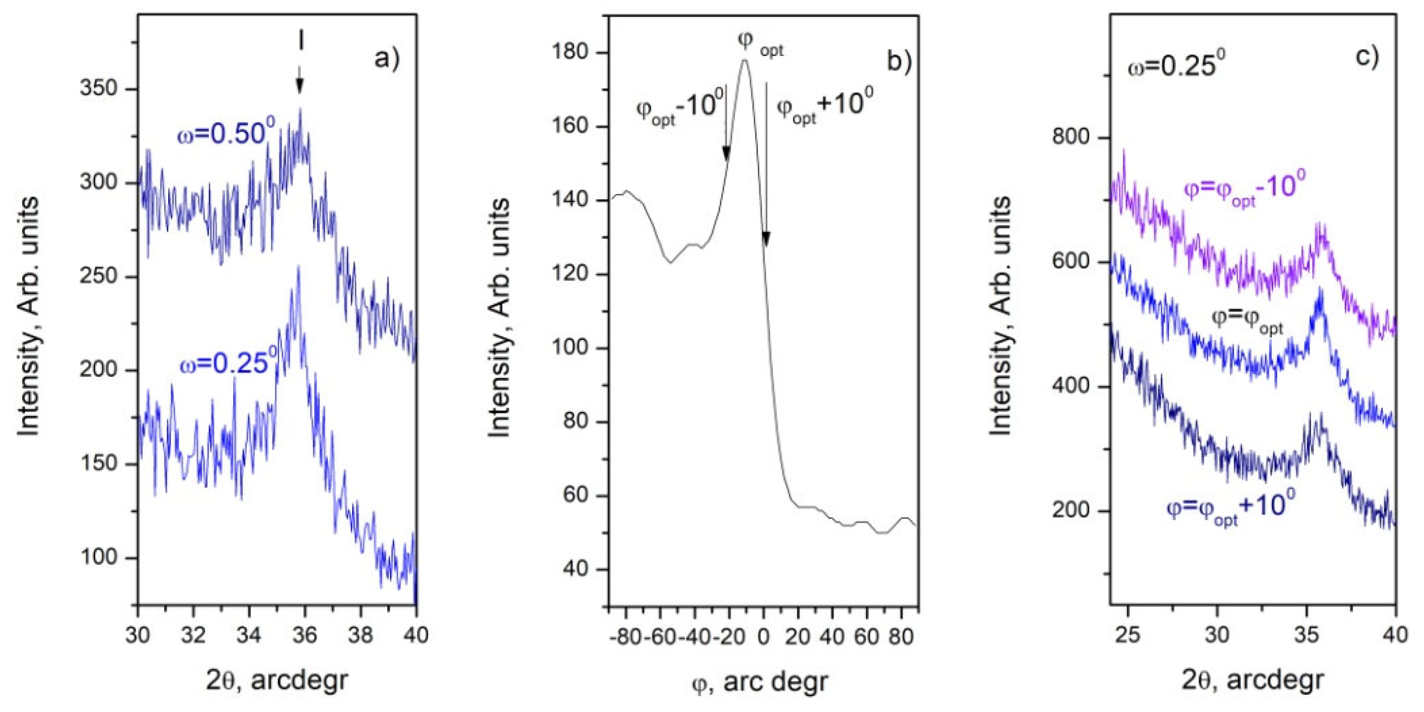
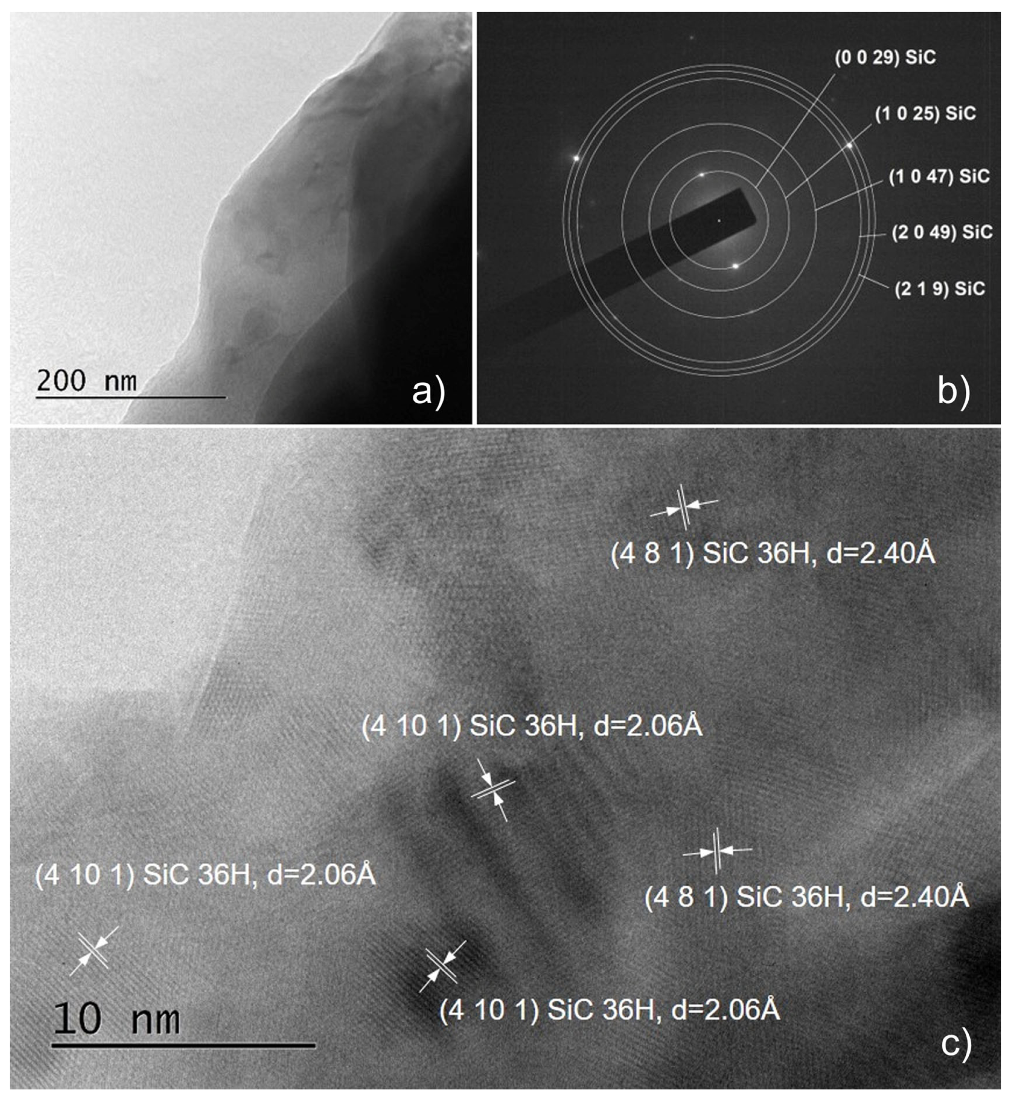
Regardless of the substrate preparation and the synthesis time, a fraction of SiC is present in the thin films. It is most likely formed in its vast part at the Si substrate/thin film interface from gas phase carbon and Si atoms from the substrate. SiC as a separate phase probably forms a continuous film only in samples cleaned according to the protocols mentioned in the experimental section. Continuous films with a well-ordered crystal structure are formed only when the synthesis time equals or exceeds 60 min. The XRD peaks from the XRD patterns and the SAED and HRTEM images taken from these experiments clearly show a well-ordered crystalline phase, and in both cases, the identified crystalline phase is of the polytype 36H–SiC.
-
The processes of permanent reconstruction of the Si(111) slab at high temperatures determine the deep penetration of C and O atoms into the substrate and the blurring of the thin film/Si-substrate interface. This gives rise to certain difficulties in measuring the thickness of these thin films. The detailed distribution of C- and O-containing species (see Figure 4a–f) unequivocally confirms that oxygen and carbon diffuse into the Si substrate, while the SiC phase predominantly remains within the thin film. This process results in the formation of a region extending from the interface into the substrate depth, where Si is doped with C and O. We assume that this region begins at the interface (or at the point where the carbon concentration decreases by 2–4% from its maximum, while the silicon concentration increases correspondingly), and it extends until the C and O concentrations stabilize at their constant residual values. Based on this, the thickness of these regions ranges from approximately 50–60 nm (for C3 samples) to over 100–110 nm (for C90 samples) (see Figure 5a,b and Figure S5d) in the samples with properly cleaned native oxides and is larger in the uncleaned samples (see Figure S5c). This also explains why no clear results are obtained when measuring the thickness of thin films synthesized in long processes (20 min or more) (see the beginning of the Section 3) using SEM, AFM, and optical profilometry. In these methods, thickness determination relies on mechanical surface scratching; however, the high concentration of C and O near the substrate surface significantly alters the silicon properties and affects thin film adhesion, preventing the scratches from accurately defining the thin film/substrate interface. Similarly, ellipsometric measurements yield slightly increased thickness values for thin films—even those with small thicknesses (up to 15 nm)—because for reasons similar to those mentioned above, the upper part of the substrate exhibits characteristics resembling those of the thin film. Consequently, the ellipsometrically determined thicknesses of samples O3, C3, O5, and C5 were 12, 12, 13.5, and 15 nm, respectively, whereas GDOS measurements determined them to be 4, 5, 7, and 8 nm. This suggests that in ellipsometric measurements, part of the heavily doped region of the Si substrate is perceived as part of the thin film.
-
As mentioned above, our experiments showed that the thin films consist of crystalline/nanocrystalline/amorphous SiC doped with some O, which is on a C and O co- doped Si- substrate. From general considerations, we can suppose that the complex composition of the thin films and highly enriched-with-C-and-O silicon area will more easily compensate for the difference in the lattice parameters of the SiC and Si substrates as well as their coefficients of thermal expansion than a monophase thin film of nanocrystalline/crystalline SiC. From this, we can conclude that the applied method is promising for depositing intermediate thin films of SiC on Si(111) using quartz equipment, i.e., compatible with the Si technology.
-
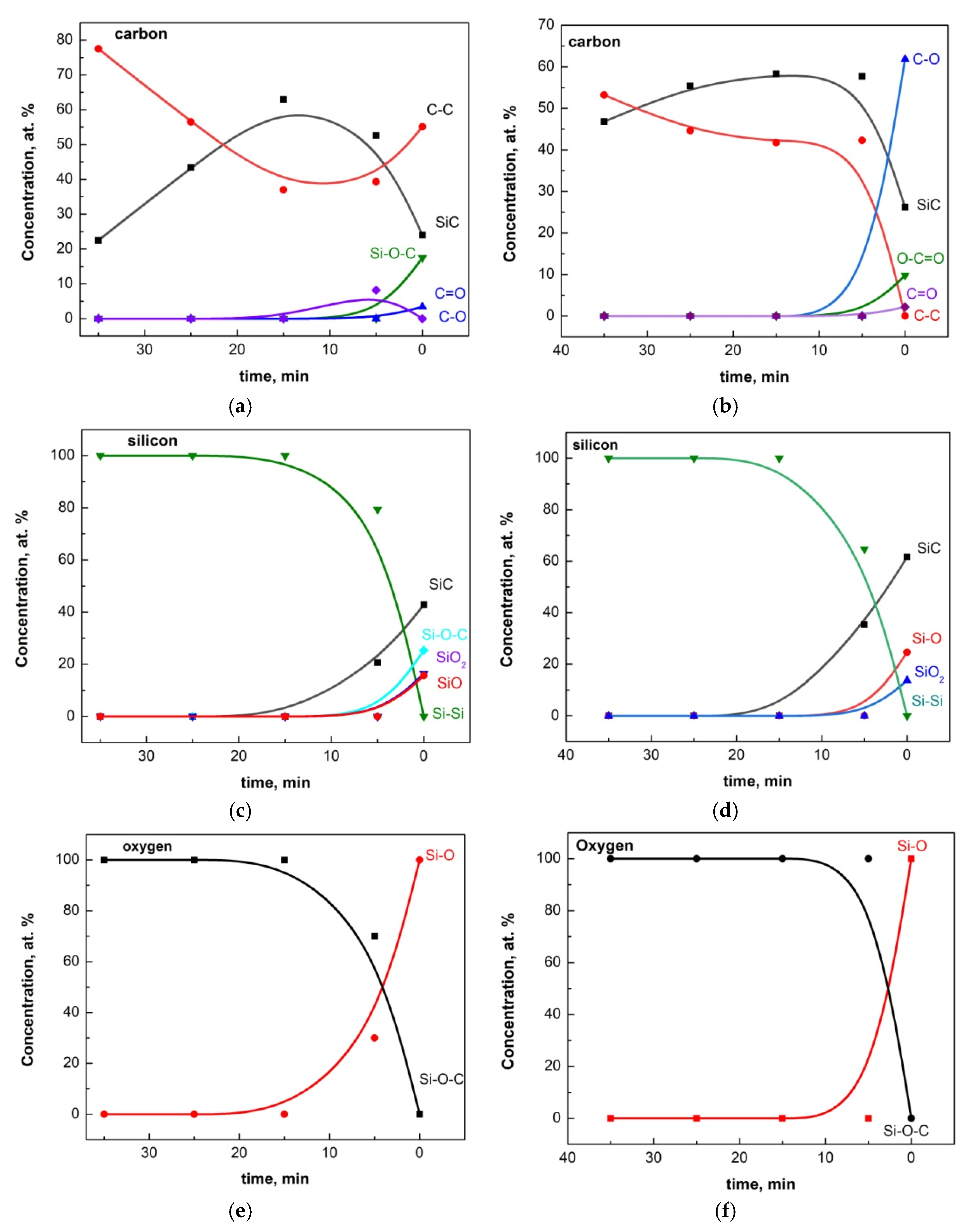
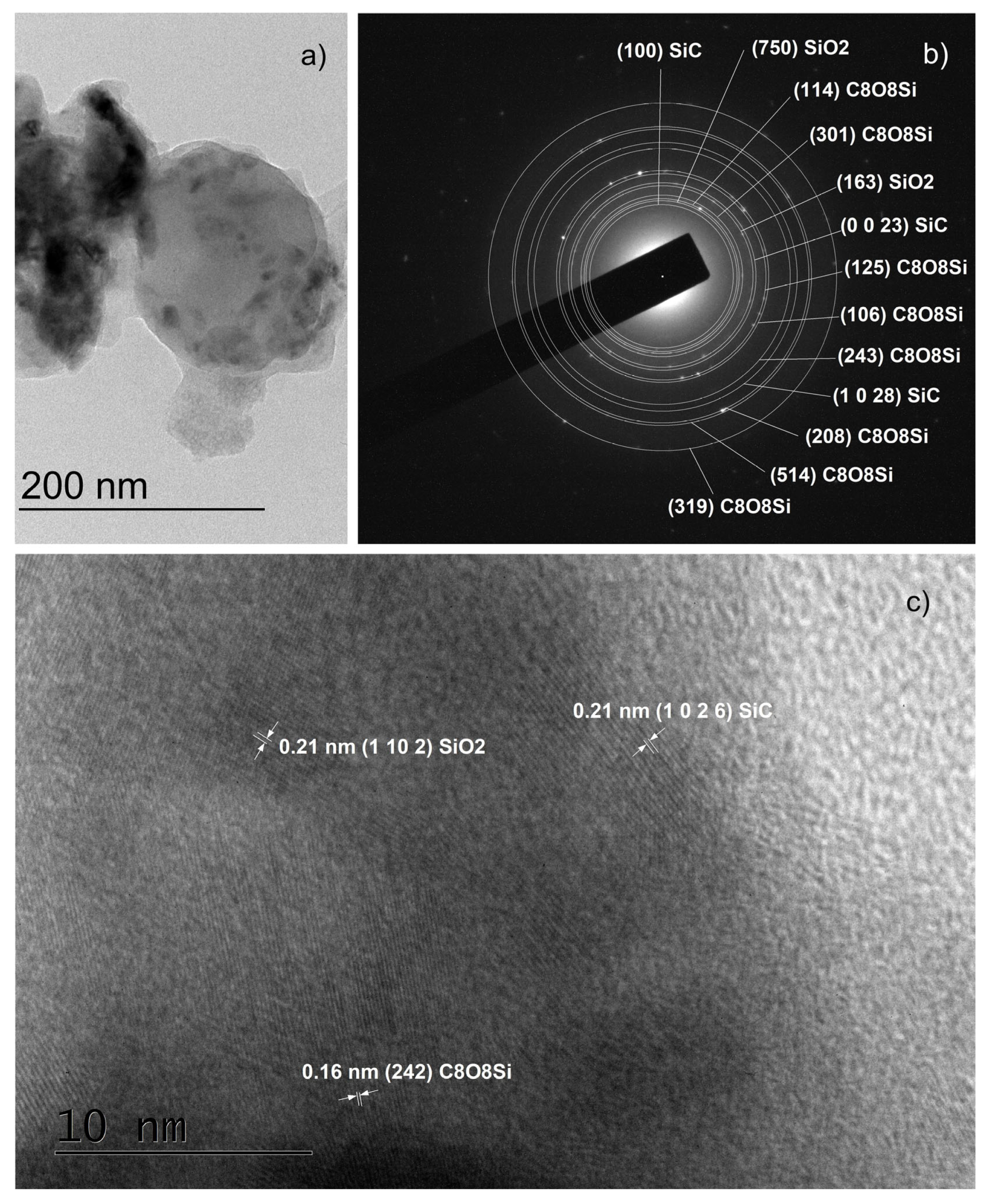
Carbon and oxygen were observed in the thin films both in the form of impurities, C, O, C–O, C=O, and Si–O–C (see the XPS results), as well as crystalline SiO2 (in the SAED and HRTEM images) and as the complex compound Si(OCOCH3)4 (in the SAED and HRTEM images). The latter compound has a low melting point of 160 °C and most likely is formed in those areas where its components were present in the necessary proportions during the cooling of the thin films. In this sense, its synthesis can be considered accidental rather than typical, and it was found only in two of the samples mentioned above. Moreover, we observed crystalline SiO2 and Si(OCOCH3)4 only in samples with improperly removed native SiO2.
-
The XPS results (see Figure 3c and Figure S3a–d) clearly indicate the presence of SiO2 in all studied samples with thin films deposited on substrates where the native oxide was not properly removed. Some of these findings are further supported by other local analysis methods (see the CAED insets and the XRD images referenced above). Although we lack X-ray data confirming crystalline or amorphous silicon oxide, powder XRD is not expected to detect such small quantities of a given phase. Therefore, we can reasonably assume that in all samples with natural oxide—following established protocols—SiO2 is present within the thin films in the form of Si–O, SiO2, and Si–O–C particles. We attribute their presence to the diffusion of residual oxygen, left after etching at 1135–1140 °C in a hydrogen (H2) flow, into the substrate during subsequent heating above 900–1000 °C. The deposition of carbon atoms and their further migration likely amplify this process.

5. Conclusions

The experimental studies conducted allow some important conclusions to be drawn. It is obvious that regardless of how the silicon substrates are cleaned, a larger or smaller amount of native silicon oxide remains on their surface, depending on the treatment. Very often the thin film of mainly amorphous or nanocrystalline SiC (at short carbonization times 3–20 min) contains up to several mass percent impurities of C, O, Si–O, C=O, and Si–O–C. At long carbonization processes the thin films are mainly of crystalline SiC (3C–SiC or 39H–SiC) but also have impurities of C, O, Si–O, C=O, and Si–O–C. The crystal grain size determined by the Scherrer equation for the thin films obtained after carbonization for 60 and 90 min is about 7 nm and about 110 nm, respectively. Just below the thin film, in the volume of the Si substrates, as a result of the diffusion of C and O in the volume, a strongly enriched C and O region is formed, extending in depth from about 50 nm (at 3 min carbonization) to about 110–120 nm (at 90 min carbonization). In cases where the native oxide is not properly removed from the Si surface, the mixture is enriched with large amounts of Si–O/Si–O–C mixed phases of up to 25 mol% for substrates with non-removed native oxide. The significant diffusion of oxygen and carbon atoms into the bulk of the Si substrate makes the thin film/substrate interface indistinguishable and greatly complicates the determination of the thickness of the thin films by methods related to scratching the surface. However, the formation near the thin film/substrate interface in the Si- substrate, a region of highly enriched with C, O, Si–O, Si=O and Si–O–C species, is expected to compensate to some extent for the difference in the lattice parameters of SiC and Si as well as the difference in their thermal expansion coefficients and to suppress the formation of mechanical defects upon cooling of the samples.

Supplementary Materials

The following supporting information can be downloaded at https://www.mdpi.com/article/10.3390/app15137078/s1. Figure S1: (a,b) Schematic representation of the experimental processes of carbonization of Si(111) substrates: (a) time distribution of the different gas flows, and (b) temperature regimes (blue trace) and the corresponding residual pressures in the reactor (red trace). Figure S2: (a–c) The XRD patterns obtained from samples C90 and O90, enlarged in the interval 2θ = (30–31.5)°, 2θ = (35–40)° and 2θ = (58–60)° (panels a, b and c, respectively). The reflections that can be ascribed to 36H–SiC [25] are indicated by the corresponding interplanar distances, while the reflections indicated by numbers should be related to 96R–SiC [26], as follows: 1 = d(00-81) and 2 = d(00-84). Strong reflections are associated with distances between crystal planes of 3.0217 Å, 2.8328 Å, 2.3244 Å, and 1.5629 Å, while the weak ones are associated with 2.9242 Å and 2.5181 Å, respectively. The reflection indicated by 3 is of unknown origin, but is very close to d(015)= 2.5636 Å of 19H–SiC which possess trigonal symmetry (SG #156 P 3m1 and cell parameters a0 = 3.0730 Å, c0 = 47.7530 Å) [28]. (d) The XRD pattern obtained from sample C90, (θ–2θ) scan, in the interval 2θ = (35–76)° used for determination of the crystal grain size. The reflection used appears at 2θ = 38.7° and corresponds to d(00-39) = 2.3244 Å [25]. The estimated grain size is about 7 nm. (e) The XRD patterns in obtained from sample C60, (θ–2θ) scan, in the interval 2θ = (30–55)° used for determination of the crystal grain size. The pattern is indexed in cubic symmetry (SG #216 F-43m and cell parameter a0 = 3.3480 Å [3] and the reflection used (at 2θ = 35.8°) corresponds to d(111) = 2.5103 Å. The estimated grain size is about 7 nm. (f) The XRD patterns in obtained from sample C60, (ω–2θ) scan, in the interval 2θ = (20–40)° used for determination of the crystal grain size. The reflection used corresponds to d(111) = 2.5103 Å [4] and the grain size is about 6.0 nm. Table S1: Chemical composition of the thin films as determined by XPS survey studies for samples C3, O3, C5, O5, O20, O60, C90, and O90. Figure S3: (a) Deconvolution of the C 1s line of sample O20. (b) Deconvolution of the C 1s line of sample O60. (c) Deconvolution of the C 1s line of sample O90; (d) Deconvolution of the C 1s line of sample C90. Figure S4: (a) Deconvolution of the Si 2p line of sample O20. (b) Deconvolution of the Si 2p line of sample O60. (c) Deconvolution of the Si 2p line of sample O90. (d) Deconvolution of the Si 2p line of sample C90. Figure S5: (a) GDOES study of O5 at different points of the specimen. The figure shows the results that differ the most, marked as O5_1 and O5_2 as well as the mass concentration of Si (blue traces), and C and O (black and red traces, respectively). (b) GDOES study of C20 specimen. The mass concentration of Si, C, and O is presented by blue, black and red traces, respectively. (c) GDOES study of O5 sample at depth interval 40–120 nm: the mass concentration of Si is drawn by blue trace, while those of C and O are drawn by black and red traces, respectively. (d) GDOES study of C90 sample at depth interval 40–120 nm: the mass concentration of Si is drawn by blue trace, while those of C and O are drawn by black and red traces, respectively. Figure S6: TEM images obtained from O20 specimen: (a) a low magnification TEM and the corresponding SAED images (inset) obtained from O20 specimen. (b) HRTEM image indicating the presence of different phases in the studied specimen. Figure S7: TEM images obtained from O90 specimen: (a) a low magnification TEM and the corresponding SAED images (inset) obtained from O90 specimen. (b) HRTEM image indicating the presence of single SiC phase. Figure S8: Raman spectra of C90 (red trace) and Si(111) substrate (black trace). Inset: Raman spectrum of the thin film (sample C90) obtained by subtracting the Raman spectrum of the bare Si(111) substrate from the spectrum of C90 specimen.

Author Contributions

Conceptualization, T.M.; Methodology, T.M.; Validation, T.M. and S.K.; Investigation, T.M., V.M., P.R., I.A., I.Z., G.A., D.K. (Daniela Karashanova), B.G., P.T., K.K., B.B., S.K., D.D., D.K. (Dobromir Kalchevski) and D.K. (Desislava Karaivanova); Writing—original draft, T.M. and I.A.; Writing—review & editing, T.M., I.A., D.K. (Daniela Karashanova) and V.P.; Supervision, T.M. and V.P.; Project administration, T.M.; Funding acquisition, T.M. All authors have read and agreed to the published version of the manuscript.

Funding

The authors gratefully acknowledge financial support from the National Science Fund of Bulgaria under Grant KP-06-H58/2-16.11.2021. This work was also supported by the European Regional Development Fund under the “Research Innovation and Digitization for Smart Transformation” program 2021–2027 under Project BG16RFPR002-1.014-0006 “National Centre of Excellence Mechatronics and Clean Technologies”. Research equipment of the Distributed Research Infrastructure INFRAMAT, part of the Bulgarian National Roadmap for Research Infrastructures, supported by Bulgarian Ministry of Education and Science was used in this investigation.

Data Availability Statement

Data is contained within the article.

Conflicts of Interest

The authors declare no conflicts of interest.

Abbreviations

The following abbreviations are used in this manuscript:
PVDPhysical Vapor Deposition
CVDChemical Vapor Deposition
UHSSUltra-High Strength Steel
XPSX-ray Photoelectron spectroscopy
GDOESGlow Discharge Optical Emission Spectroscopy
XRDX-ray Diffraction
GIXRDGrazing Incidence X-ray diffraction
TEMTransmission Electron Microscopy
HRTEMHigh-Resolution Transmission Electron Microscopy
SAEDSelected Area Electron Diffraction

References

  1. Acheson, E.G. Process of Making Graphite. U.S. Patent # US 711031, 14 October 1902. [Google Scholar]
  2. Xu, X.; Hu, X.; Chen, X. SiC Single Crystal Growth and Substrate Processing. In Light-Emitting Diodes; Solid State Lighting Technology and Application Series; Li, J., Zhang, G.Q., Eds.; Springer: Cham, Switzerland, 2019; Volume 4. [Google Scholar]
  3. Rebecca, C. Silicon Carbide Microelectromechanical Systems for Harsh Environments; Imperial College Press: London, UK, 2006; p. 3. ISBN 1-86094-624-0. [Google Scholar]
  4. Käckell, B.; Wenzien, F.B. Electronic properties of cubic and hexagonal SiC polytypes from ab initio calculations. Phys. Rev. B 1994, 50, 10761. [Google Scholar]
  5. Nishino, S.; Powell, J.A.; Will, H.A. Production of large-area single-crystal wafers of cubic SiC for semiconductor devices. Appl. Phys. Lett. 1983, 42, 460. [Google Scholar]
  6. Severino, A.; D’Arrigo, G.; Bongiorno, C.; Scalese, S.; La Via, F.; Foti, G. Thin crystalline 3C-SiC layer growth through carbonization of differently oriented Si substrates. J. Appl. Phys. 2007, 102, 023518. [Google Scholar] [CrossRef]
  7. Kukushkin, S.A.; Osipov, A.V. New method for growing silicon carbide on silicon by solid-phase epitaxy: Model and experiment. Phys. Solid State 2008, 50, 1238. [Google Scholar] [CrossRef]
  8. Deura, M.; Fukuyama, H. Formation of SiC layer by carbonization of Si surface using CO gas. J. Cryst. Growth 2016, 434, 77. [Google Scholar] [CrossRef]
  9. Kukushkin, S.A.; Osipov, A.V. Quantum mechanical theory of epitaxial transformation of silicon to silicon carbide. J. Phys. D Appl. Phys. 2017, 50, 464006. [Google Scholar] [CrossRef]
  10. Kukushkin, S.A.; Osipov, A.V. Nanoscale Single-Crystal Silicon Carbide on Silicon and Unique Properties of This Material. Inorg. Mater. 2021, 57, 1319. [Google Scholar] [CrossRef]
  11. Kukushkin, S.A.; Markov, L.K.; Pavlyuchenko, A.S.; Smirnova, I.P.; Osipov, A.V.; Grashchenko, A.S.; Nikolaev, A.E.; Sakharov, A.V.; Tsatsulnikov, A.F.; Sviatets, G.V. SiC/Si Hybrid Substrate Synthesized by the Method of Coordinated Substitution of Atoms: A New Type of Substrate for LEDs. Coatings 2023, 13, 1142. [Google Scholar] [CrossRef]
  12. Molina, S.I.; Morales, F.M.; Araújo, D. SiC thin films obtained by Si carbonization. Mater. Sci. Eng. B 2001, 80, 342–344. [Google Scholar] [CrossRef]
  13. Severino, A.; Bongiorno, C.; Leone, S.; Mauceri, M.; Pistone, G.; Condorelli, G.; Abbondanza, G.; Portuese, F.; Foti, G.; La Via, F. Carbonization Study of Different Silicon Orientations. Mater. Sci. Forum 2007, 556–557, 171–174. [Google Scholar] [CrossRef]
  14. Sato, H.; Goto, T.; Okuno, A.; Yoshikawa, A. Preparation of SiC coatings on graphite substrates via CVD using polysilaethylene. J. Cryst. Growth 2025, 649, 127931. [Google Scholar] [CrossRef]
  15. Steiner, J.; Schultheiß, J.; Wang, S.; Wellmann, P.J. Fabrication of SiC-on-Insulator (SiCOI) Layers by Chemical Vapor Deposition of 3C-SiC on Si-in-Insulator Substrates at Low Deposition Temperatures of 1120_C. Crystals 2023, 13, 1590. [Google Scholar] [CrossRef]
  16. Kablov, E.N.; Kuznetcov, N.T.; Sarkisov, P.D.; Graschenkov, D.V.; Sevast’yanov, V.G.; Orlova, L.A.; Simonenko, E.P. Method for Protecting Carbon-Containing Materials with Silicon Carbide. Patent RU 2350580, 27 March 2009. [Google Scholar]
  17. Shikunov, S.; Kaledin, A.; Shikunova, I.; Straumal, B.; Kurlov, V. Novel Method for Deposition of Gas-Tight SiC Coatings. Coatings 2023, 13, 354. [Google Scholar] [CrossRef]
  18. Chen, B.Y.; Chi, C.C.; Hsu, W.K.; Ouyang, H. Synthesis of SiC/SiO2 core–shell nanowires with good optical properties on Ni/SiO2/Si substrate via ferrocene pyrolysis at low temperature. Sci. Rep. 2021, 11, 233. [Google Scholar] [CrossRef]
  19. Koo, J.; Chinkyo Kim, C. A new critical growth parameter of H2/CH4 gas flow ratio and mechanistic model for SiC nanowire synthesis via Si substrate carbonization. Sci. Rep. 2024, 14, 29629. [Google Scholar] [CrossRef]
  20. Liu, H.; Zhang, X.; Xu, N.; Han, C.; Wu, N.; Wang, B.; Wang, Y. Progress of One-Dimensional SiC Nanomaterials: Design, Fabrication and Sensing Applications. Nanomaterials 2024, 14, 187. [Google Scholar] [CrossRef]
  21. Yang, X.; Liu, R.; Liu, B.; Liu, M. Synthesis of Ultra-Thin Two-Dimensional SiC Using the CVD Method. Energies 2022, 15, 6351. [Google Scholar] [CrossRef]
  22. Kalchevski, D.A.; Trifonov, D.V.; Kolev, S.K.; Aleksandrov, H.A.; Milenov, T.I. Ab initio study of the mechanism of carbonization of {111} Si-substrate at high temperature. Mater. Chem. Phys. 2024, 317, 129180. [Google Scholar]
  23. The University of Texas at El Paso, Nanofabrication Facility. Available online: https://www.utep.edu/engineering/nanomil/processes/cleaning.html (accessed on 25 April 2025).
  24. The Integrated Nanosystems Research Facility at The University of California, Irvine. Available online: https://www.inrf.uci.edu/wordpress/wp-content/uploads/sop-wet-silicon-solvent-clean.pdf (accessed on 25 April 2025).
  25. Krishna, P.; Verma, A.R. A novel determination of the structure of an anomalous polytype of silicon carbide. Acta Crystallogr. 1964, 17, 51–57. [Google Scholar] [CrossRef]
  26. Singh, G.; Verma, A.R. The structure of a new silicon carbide polytype 96R. Acta Crystallogr. 1964, 17, 49–51. [Google Scholar] [CrossRef]
  27. Ramsdell, L.S.; Mitchell, R.S. Studies on Silicon Carbide. Am. Mineral. 1947, 32, 64–82. [Google Scholar]
  28. Braekken, H. Zur Kristallstruktur des kubischen Karborunds. Z. Krist. 1930, 75, 572–573. [Google Scholar]
  29. Scherrer, P. Bestimmung der Grösse und der inneren Struktur von Kolloidteilchen mittels Röntgenstrahlen. Nachr. Ges. Wiss. Göttingen 1918, 26, 98–100. [Google Scholar]
  30. National Institute of Standards and Technology. NIST X-Ray Photoelectron Spectroscopy Database; National Institute of Standards and Technology: Gaitherburg, MD, USA, 1997.
  31. Önneby, C.; Pantano, C.G. Silicon oxycarbide formation on SiC surfaces and at the SiC/SiO2 interface. J. Vac. Sci. Technol. A 1997, 15, 1597. [Google Scholar] [CrossRef]
  32. University of Twente, Mesa+ Institute, The Netherlands. Available online: https://www.utwente.nl/en/mesaplus/nanolab/analysis/nanolab-mc-pictures/xps-application-depth-profiling.pdf (accessed on 25 April 2025).
  33. Foster, M.D.; Treacy, M.M.J.; Higgins, J.B.; Rivin, I.; Balkovsky, E.; Randall, K.H. A systematic topological search for the framework of ZSM-10. J. Appl. Crystallogr. 2005, 38, 1028–1030. [Google Scholar] [CrossRef]
  34. Kamenar, B.; Bruvo, M. Lattice parameters and space groups of the acetates of IVb group elements. Acta Crystallogr. B 1972, 28, 321. [Google Scholar] [CrossRef]
  35. Nakashima, S.; Harima, H. Raman Investigation of SiC Polytypes. Phys. Status Solidi A 1997, 162, 39. [Google Scholar] [CrossRef]
  36. Ferrari, A.; Basko, D. Raman spectroscopy as a versatile tool for studying the properties of graphene. Nat. Nanotechnol. 2013, 8, 235. [Google Scholar] [CrossRef]
  37. Ferrari, A.C.; Robertson, J. Raman spectroscopy of amorphous, nanostructured, diamond-like carbon, and nanodiamond. Philos. Trans. R. Soc. Lond. A 2004, 362, 2477. [Google Scholar] [CrossRef]
Figure 1. XRD patterns taken from the C3, C5, C60, C90, and O90 samples drawn in green, violet, blue, black, and red traces, respectively. The inset presents a magnified area around the d(111) reflection marked with I on the XRD patterns of samples C3, C5, and C60 drawn in green, violet, and blue traces, respectively.
Applsci 15 07078 g001
Figure 2. The GIXRD study of the C60 sample: (a) GIXRD taken in (ω−2θ) scans at ω = 0.25° (upper trace) as well as at ω = 0.50° (lower trace); (b) GIXRD taken in φ scans in the range φ = (0–180)° regarding d(111) of 3C–SiC at 2θ = 35.6° [28]; (c) GIXRD taken in (ω−2θ) scans taken at φopt as well as (φopt − 10°) and (φopt + 10°) and ω = 0.25°.
Applsci 15 07078 g002
Figure 3. (a) The deconvolution of the C 1s line of sample O3. (b) The deconvolution of the C 1s line of sample C3. (c) The deconvolution of the Si 2p line of sample O3. (d) The deconvolution of the Si 2p line of sample C3.
Applsci 15 07078 g003
Figure 4. (a) The in-depth distribution of C-containing species in sample O3 according to the deconvolution of the C 1s line. (b) The in-depth distribution of C-containing species in sample O5 according to the deconvolution of the C 1s line. (c) The in-depth distribution of Si-containing species in sample O3 according to the deconvolution of the Si 2p line. (d) The in-depth distribution of Si-containing species in sample O5 according to the deconvolution of the Si 2p line. (e) The in-depth distribution of O-containing species in the sample O3 according to the deconvolution of the O 1s line. (f) The in-depth distribution of O-containing species in sample O3 according to the deconvolution of the O 1s line.
Applsci 15 07078 g004
Figure 6. TEM images obtained from C3 samples: (a) A low magnification TEM image and the corresponding SAED image (b); HRTEM images (c,d) of different areas of panel (a).
Applsci 15 07078 g006
Figure 7. TEM images obtained from sample O5: a low magnification TEM and the corresponding SAED images (panels (a,b)) and HRTEM image indicating the presence of different phases in the studied sample (panel (c)).
Applsci 15 07078 g007
Figure 8. TEM images obtained from sample C60: a low magnification TEM and the corresponding SAED images (see inset) (panel (a)) and HRTEM image indicating the presence of a single SiC phase (panel (b)).
Applsci 15 07078 g008
Figure 9. TEM images obtained from sample C90: an overview image of a micro-sized sample particle; a large part of the surrounding space (panel (a)), the corresponding SAED (panel (b)) images; and HRTEM images showing well-structured SiC nanocrystals (panel (c)).
Applsci 15 07078 g009
Table 1. The summarized data on the experimental conditions of the various experiments and the thicknesses of the deposited films.
ExperimentPlasma
Etching
Deposition Time (min)CH4 Gas Flow (sccm)
C3 +1 × 310
O3+1 × 310
C5+1 × 510
O5+1 × 510
C20 +1 × 2010
O20+1 × 2010
C60+1 × 6010
O60+1 × 6010
C90 +1 × 9010
O90 +1 × 9010
Disclaimer/Publisher’s Note: The statements, opinions and data contained in all publications are solely those of the individual author(s) and contributor(s) and not of MDPI and/or the editor(s). MDPI and/or the editor(s) disclaim responsibility for any injury to people or property resulting from any ideas, methods, instructions or products referred to in the content.

