Article

A CMOS-Based Terahertz Reconfigurable Reflectarray with Amplitude Control: Design and Validation

1
Department of Electronic Engineering, Tsinghua University, Beijing 100084, China
2
State Key Laboratory of Space Network and Communications, Tsinghua University, Beijing 100084, China
*
Author to whom correspondence should be addressed.
Appl. Sci. 2025, 15(12), 6638; https://doi.org/10.3390/app15126638
Submission received: 30 March 2025 / Revised: 5 June 2025 / Accepted: 11 June 2025 / Published: 12 June 2025
(This article belongs to the Special Issue Recent Advances in Reflectarray and Transmitarray Antennas)

Abstract

:
Terahertz reconfigurable reflectarray antennas (RRAs) hold significant promise for next-generation wireless communication systems by enabling dynamic beam control to mitigate severe path loss at high frequencies. This work presents a Complementary Metal-Oxide-Semiconductor (CMOS)-based RRA for terahertz amplitude control using tunable split-ring resonators. First, a terahertz switch in standard 65 nm CMOS process is designed, tested, and calibrated on the chip to extract the equivalent impedance, enabling precise RRA element design. Next, a reconfigurable element architecture is presented through the co-design of a split-ring radiator, control line, and a single switch. Experimental characterization demonstrates that the fabricated RRA achieves 3 dB amplitude variation at 0.290 THz with <8.5 dB element loss under 0.8 V gate bias. The measured results validate that the proposed single-switch topology effectively balances reconfigurability and loss performance in the terahertz regime. The demonstrated CMOS-compatible RRA provides a scalable solution for real-time beamforming in terahertz communication systems.

1. Introduction

The terahertz (THz) frequency range (0.1 THz to 10 THz) holds immense potential for next-generation high-speed wireless communication, sensing, and imaging applications [1,2,3,4]. However, the severe free-space path loss of THz waves necessitates the development of high-gain beamforming with agile reconfigurability to adapt to dynamic channel conditions [5]. Traditional approaches, such as mechanical beam-steering [6] and phased arrays [7,8], face limitations in THz regimes: mechanical systems suffer from high processing accuracy, complex servo system and slow scanning speed, while the traditional phased arrays require complex feeding networks and expensive active components. Alternatively, reconfigurable metasurfaces consists of subwavelength-scale tunable meta-units that enable agile wavefront modulation [9], offering advantages such as high integration, low cost, and low power consumption compared to traditional phased arrays [10,11]. Therefore, reconfigurable metasurfaces have emerged as a promising technology for enabling high gain and programmable wireless environments in future networks [12,13].
Reconfigurable metasurfaces typically rely on tuning devices such as a Complementary Metal-Oxide-Semiconductor (CMOS) [14,15,16,17], High Electron Mobility Transistor (HEMT) [18,19,20,21,22], graphene [23,24,25,26], liquid crystals [27,28,29,30], vanadium dioxide (VO₂) [31,32,33,34], and Micro-Electro-Mechanical Systems (MEMS) [35,36] to dynamically control the surface current distribution of subwavelength periodic structures and the amplitude and phase change in electromagnetic waves. In the sub-THz band, HEMT devices generally achieve higher operating frequencies and lower noise than CMOS, yet face challenges in large-scale integration and higher fabrication complexity [20]. Graphene and liquid crystals, as tunable materials, are not limited by the cutoff frequencies of CMOS and HEMT devices and offer broad operational bandwidth, making them valuable for terahertz wave modulation. However, graphene faces challenges in fabrication and reliability for large-scale integration [24], while liquid crystals require high driving voltages and exhibit slow response times [28]. Other phase change materials, such as VO₂, are also candidate solutions for terahertz signal control [32]. They respond not only to electrical stimuli but also to thermal excitation, though their response times remain significantly slower than semiconductor-based approaches. Compared to CMOS processes, these control methods are often troubled by the difficulty of controlling each element individually and scaling up to large sizes in THz applications. MEMS enable terahertz wave manipulation by physically reconfiguring the metasurface structure [35,36]. Compared to semiconductor-based methods, MEMS offer advantages such as low insertion loss and wide bandwidth, but suffer from limited operational lifetime.
In this context, silicon-based CMOS technology presents a better solution [14,15,16,17]. Mature CMOS processes, capable of micron-level precision, are suitable for fabricating THz metasurface element structures. Additionally, CMOS-based approaches offer multilayer interconnect capabilities and mass production feasibility, enabling individual element control and large-scale scalability, making them ideal for metasurface fabrication. Due to the parasitic characteristics of CMOS processes in high-frequency bands, it is unavoidable that the performance of terahertz switches decreases. One notable development used the parallel inductive loops for resonance with the parasitic capacitance for switch performance improvement [15]. The CMOS-based reconfigurable transmitarray antenna (RTA) [15] operated at 300 GHz with an eight-switch integrated metasurface element. Another CMOS-based RRA [16,17], fabricated by advanced 22 nm process, employed two integrated Fin Field-Effect Transistor (FinFET)s as a polarization conversion method. A ±45° beam scanning range is achieved at 265 GHz. However, integrating too many switches into the metasurface element makes it difficult to enhance element efficiency.
To verify that the single switch topology can enable a RRA element to regulate THz waves at low loss levels, we propose a design concept for THz wave RRA elements and experimentally demonstrate their amplitude control capability. The element consists of a split-ring resonator, a control line, and a single switch. The equivalent impedance of the tunable switch is extracted through probe testing and Thru-Reflect-Line (TRL) calibration testing. The design approach of the RRA element enables the resonance frequency of the split-ring to be regulated by the impedance changes in the switch. Therefore, a 30 × 24-element prototype is designed, fabricated, and measured to verify the design concept. The main novelty of this work is the application of lower-frequency RRA element design methodologies in the terahertz band, achieving low-loss amplitude control of terahertz waves using CMOS technology. The remainder of this paper is organized as follows. Section 2 introduces the design concept and the RRA element structure is proposed in Section 3. Section 4 shows the fabrication and measurement of the 30 × 24 prototype. Finally, the conclusion is given in Section 5, and defining abbreviations is given in the Abbreviations section.

2. Design Concept

The reconfigurable reflectarray (RRA) element with a single switch is the simplest form of metasurface element and can be modeled as a two-port microwave network [37,38,39,40], as shown in Figure 1a,b. Port 1 is the spatial wave port, and Port 2 is the switch port. The elements are divided into the tunable switch and the passive part. The switch is typically assumed to have ideal switching characteristics, with its impedance exhibiting significant variation. The passive part of the element can be equivalent to a two-port scattering parameter matrix, used to describe the response of the element’s metallic structure and dielectric material to electromagnetic waves, and is typically regarded as a lossless network in the microwave and millimeter wave bands. In this lossless network, Port 1 matching is equivalent to Port 2 matching. Therefore, the lower-frequency RRA element design methodologies aim to design the passive part of the element so that the characteristic impedance of Port 2 is matched with the switch-related impedance. More specifically, when the characteristic impedance of Port 2 matches the impedance of the switch in ON or OFF state at a certain frequency point, the spatial wave Port 1 is simultaneously matched. Thus, the resonance of the element is achieved near that frequency point, causing the magnitude of the element reflection coefficient Γ to significantly low. When the switch is toggled to the other state, the impedance of the switch shifts dramatically, disrupting the impedance matching and the resonance. Therefore, the magnitude of the element reflection coefficient Γ remains high, thereby achieving amplitude control of the RRA element through switch operation.
As the operating frequency increases to terahertz, the performance of switches deteriorates due to high-frequency parasitics, making it impossible to achieve the ideal OFF effects. The deterioration of switch performance not only leads to an increase in element loss but also makes the design of elements more challenging. Since the characteristic impedance parameters of the switch are often complex numbers, the design goal for the element becomes unclear. Additionally, the significant material losses in the terahertz frequency range prevent the two-port network from being treated as lossless.
To address these challenges in the THz band, necessary adjustments must be made based on the lower-frequency RRA element design methodologies mentioned earlier. Since the passive part of the terahertz RRA element constitutes a lossy two-port network, simultaneous conjugate matching at both port interfaces becomes unachievable. In this case, priority must be given to ensuring conjugate matching at Port 1. It should be noted that this approach does not require conjugate matching between Port 1 input impedance and the spatial wave impedance. Instead, when Port 1 is terminated with the spatial wave impedance, the Port 2 characteristic impedance is calculated and conjugate-matched to the switch-related impedance. These two matching approaches are not equivalent in lossy networks, as will be demonstrated through numerical examples and analysis in the next section. Concretely, the design of amplitude-control RRA element has a clear goal: the passive part of the element must be designed to achieve conjugate matching between the Port 2 characteristic impedance (calculated under the condition of Port 1 matching) and the switch impedance in either the ON or OFF state.

3. Element Design

The design of a single-switch RRA element is typically divided into passive and active parts. The design of the passive part depends on the equivalent parameters of the switch, which serves as the active part. These steps are crucial for achieving amplitude control RRA in the terahertz band.

3.1. CMOS-Based Switch Design and Parameter Extraction

In standard CMOS processes, equivalent modeling of switches is typically accurate below 30 GHz. Foundries generally do not provide models for switch devices in the high-frequency range, especially in the terahertz range. This makes the design and verification of the equivalent parameters for a terahertz switch a necessary procedure.

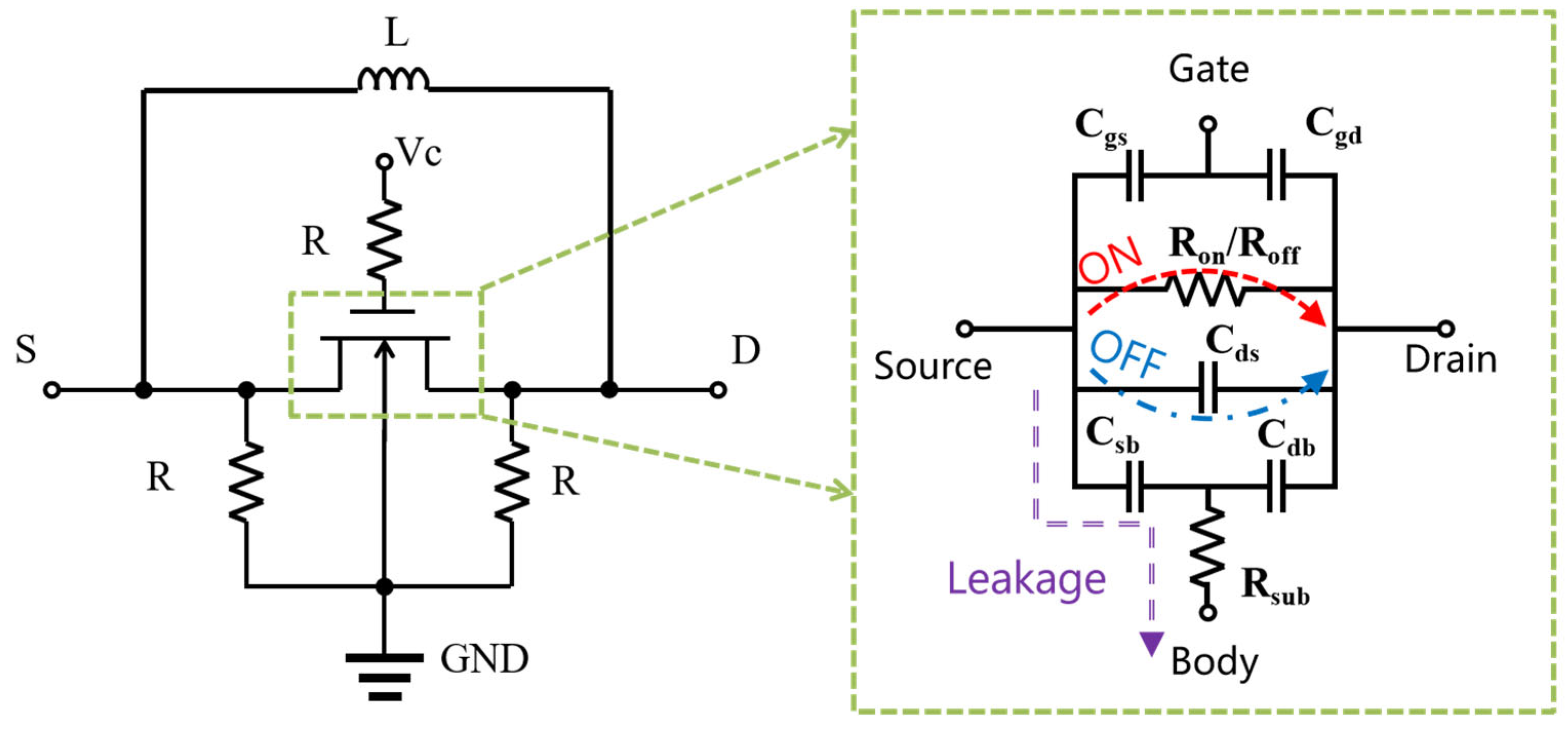
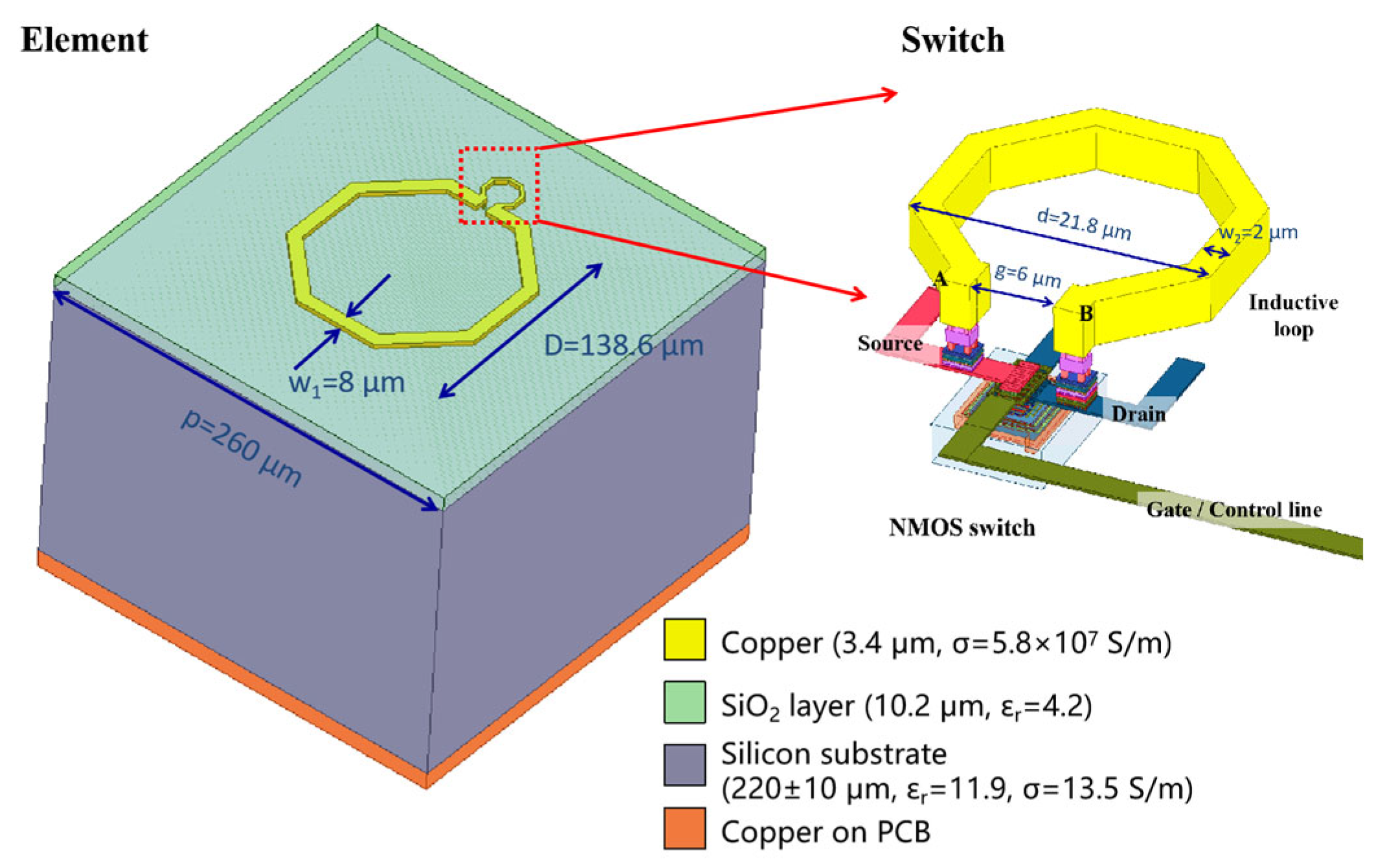
3.1.1. Switch Design

Transistors based on CMOS technology exhibit parasitic capacitance effects in the terahertz frequency range. This phenomenon prevents the switch from shutting off in the OFF state, resulting in significant leakage. Therefore, a parallel inductor is usually employed to form a resonance with the parasitic capacitance at the operating frequency [41], converting the circuit into a high-impedance path and thus achieving the desired turn-off functionality.
A custom-designed inductive loop is constructed to generate the necessary inductance in the M9 layer, enabling resonance with the transistor’s parasitic capacitance, as illustrated in Figure 2. The switch’s equivalent impedance parameters change depending on the gate voltages of 0 V and 0.8 V. An inductor loop is equivalent to an inductance L. The inductive loop is connected to the source and drain terminals of the N-channel Metal-Oxide-Semiconductor (NMOS) transistor. The gate resistor is used to reduce THz signal leakage. The ground resistors at the source and gate of the switch are placed to prevent floating potential. In Figure 2, Ron and Roff represent the equivalent source and drain resistances of the transistor under ON or OFF states in post-simulation results, including channel resistance and parasitic resistances.
As illustrated in the transistor’s small-signal model, in the OFF state, the complex parasitic capacitance can resonate with the external inductance L, presenting a high-impedance state. The equivalent parasitic capacitance in the OFF state (Coff) can be derived as:
C off = C ds + C gs C gd C gs + C gd + C sb C db C sb + C db .
The values of the parasitic capacitances can refer to the post-simulation results of the transistor. To achieve resonance at the frequency of interest f, the required inductance value L is determined by
L = 1 ( 2 π f ) 2 C off .
In the ON state, the low-impedance path provided by Ron replaces the impedance path formed by the parasitic capacitance. The source and drain terminals of the parallel inductive loop are directly connected to the switch’s source and drain. The entire switch can be integrated with the RRA element design on the M9 layer using the source (S) and drain (D) terminals.
In the THz switch design, the dimensions of the inductive loop and the transistor are critical parameters determining switch working frequency. The inductance of the loop is related to its diameter and can be obtained through full-wave electromagnetic simulation. The required inductance for resonance is given by Equation (2). The size of a transistor is usually scaled up by increasing the number of fingers, resulting in an equivalent parallel transistor configuration. This configuration reduces the resistance (Ron) in the ON state, while simultaneously increasing the parasitic capacitance (Coff) in the OFF state. Although larger transistor dimensions may degrade the switch OFF-state performance, Equation (2) demonstrates that the increased Coff actually reduces the required inductance for resonance at the working frequency. This allows for more compact inductor sizing while avoiding excessive space consumption, which is particularly valuable for RRA element design.
In summary, for switch design in terahertz RRA elements, the process involves the following: first evaluating the appropriate size range of the inductor loop based on the sub-wavelength period of the RRA element; then selecting suitable transistor dimensions to achieve resonance near the target frequency; and finally determining the optimal loop diameter according to the specific transistor dimensions.

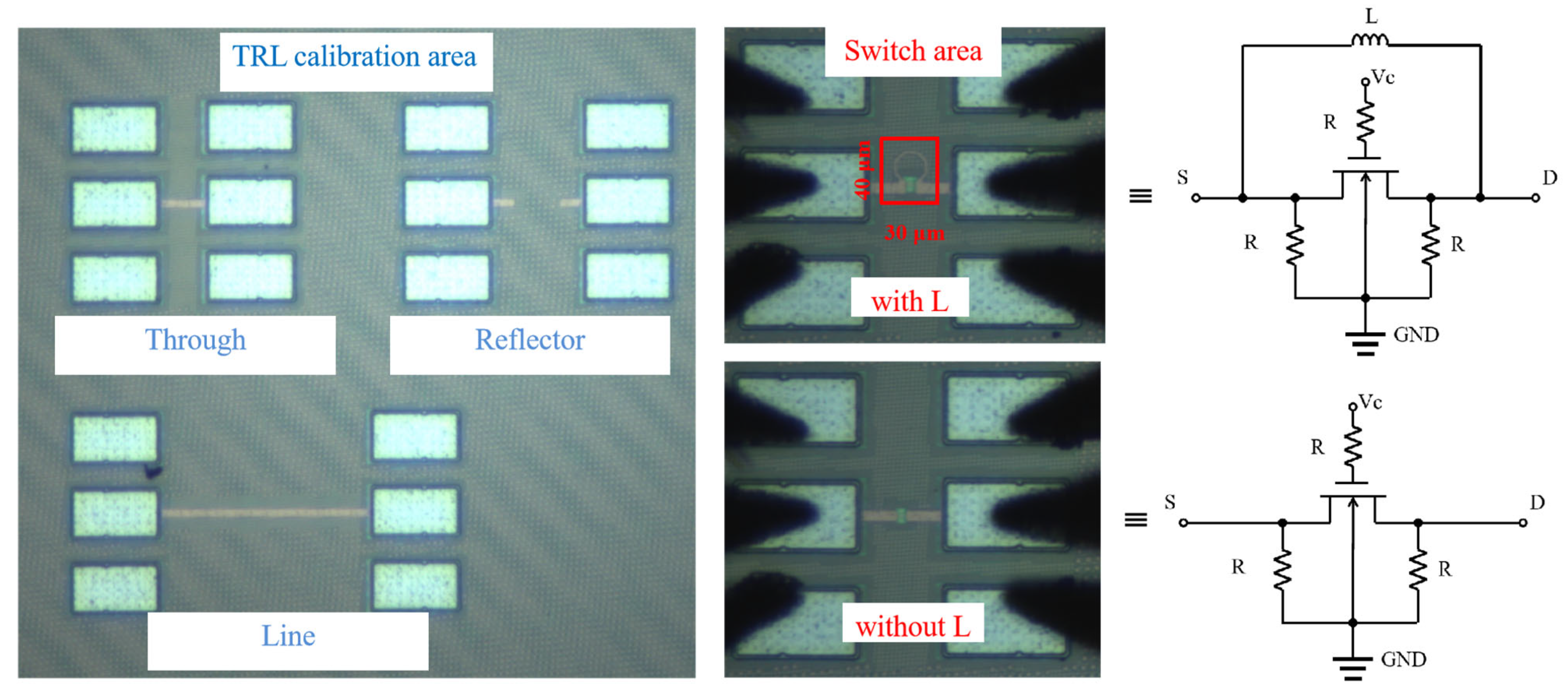
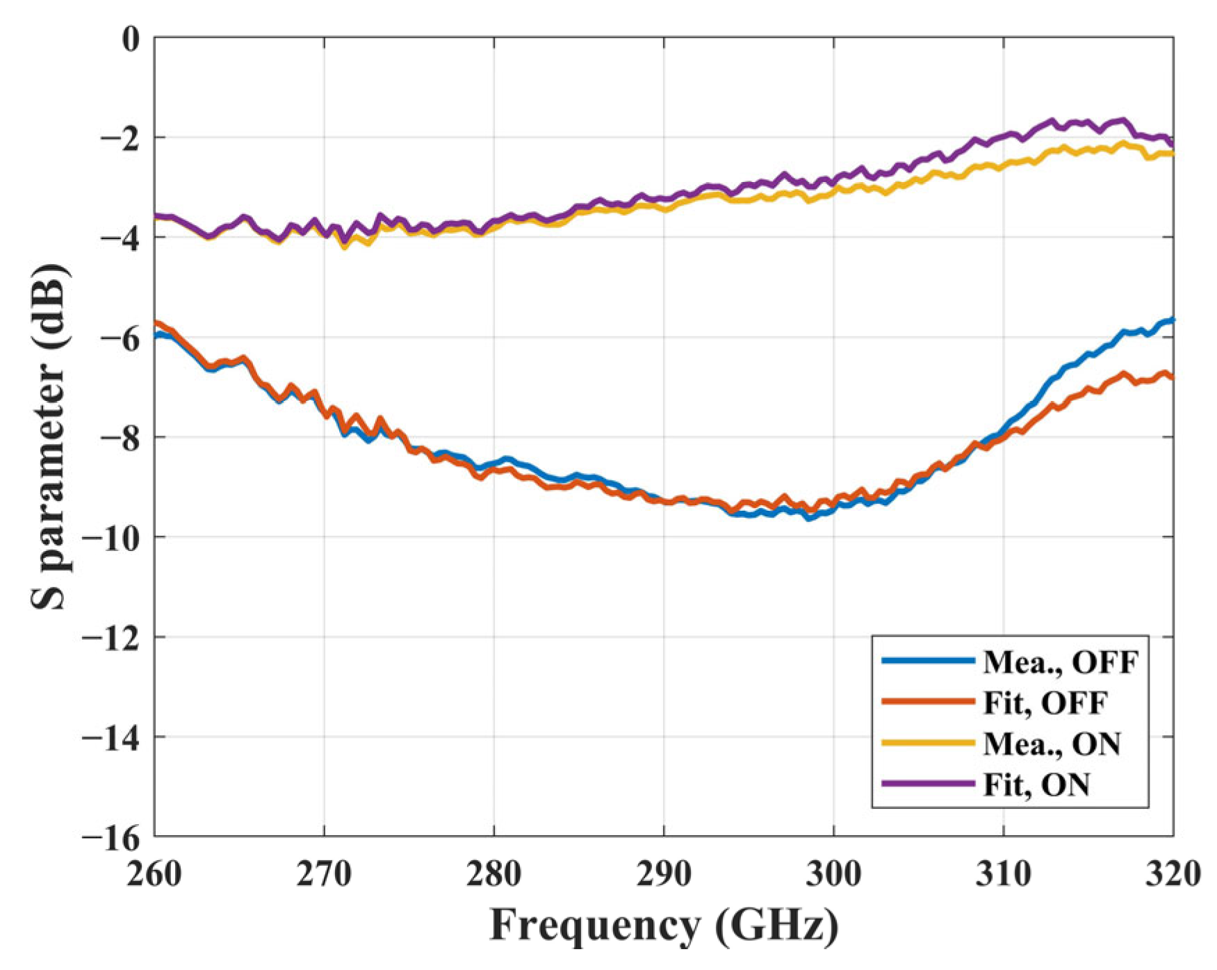
3.1.2. Switch Test and Calibration

Probe test is employed, combined with TRL calibration test, to obtain the accurate S-parameters of the switch in the THz frequency band. Figure 3 presents chip photographs of the switch area and the TRL area. The figure illustrates two fabricated switches, one incorporating an inductive loop and the other without. By comparing the S-parameters of switches with and without an inductive loop, the accurate inductance value L can be obtained.
Excluding the probe pads, the switch measures 30 μm × 40 μm. The chip probe testing is conducted using an R&S 24-GHz vector network analyzer (VNA), an R&S extension module operating in the range of 220 to 330 GHz, and SUNV WR-3 waveguide-type ground–signal–ground (GSG) probes [42]. The calibration process is performed using a self-designed TRL calibration module on a CMOS chip.

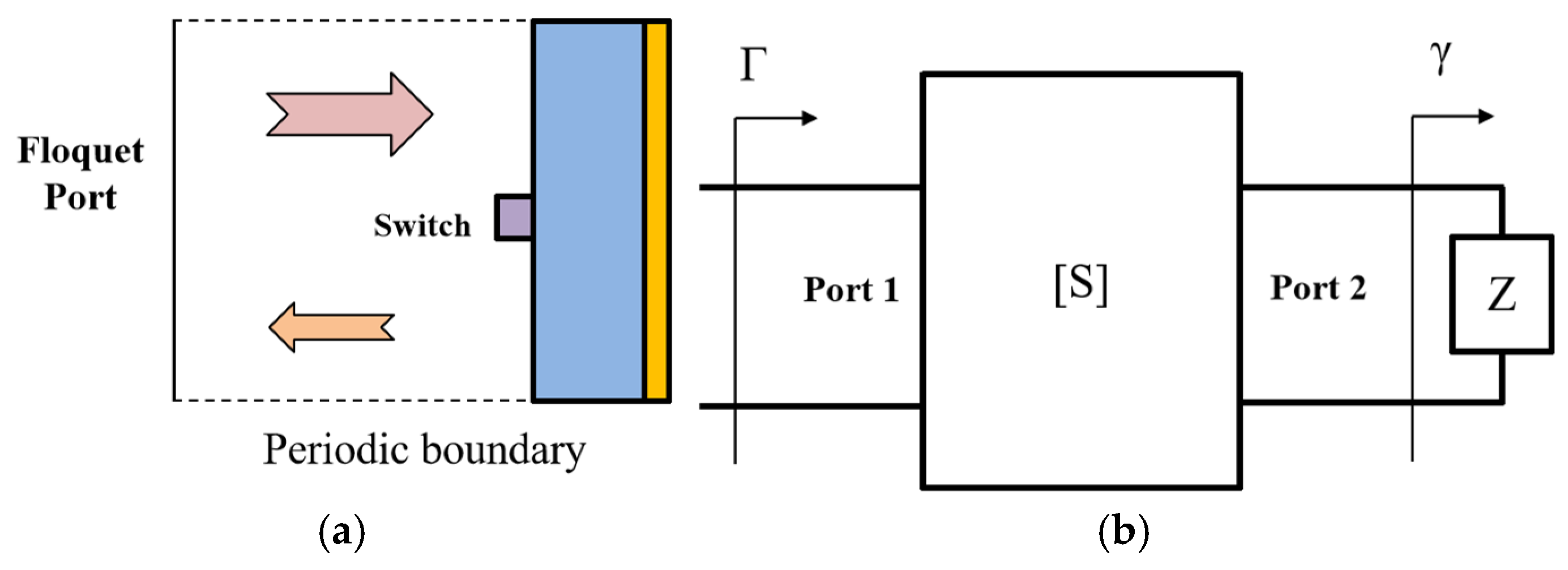
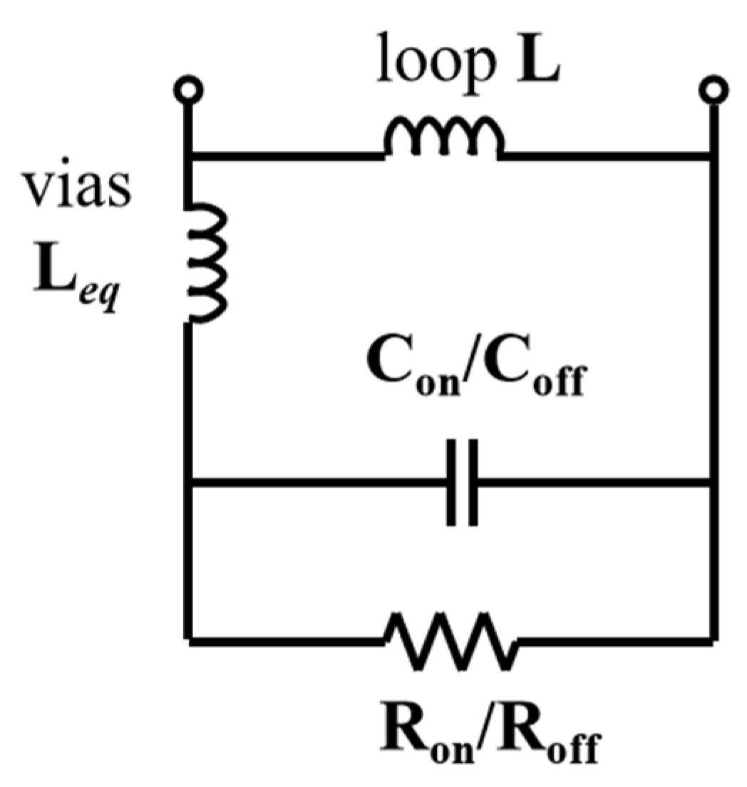
3.1.3. Switch Parameter Extraction

Terahertz switches applied on metasurfaces are equivalent to single-port devices, as shown in Figure 4. The parasitic capacitance values of the transistor are named Con and Coff, which are in a parallel configuration with the channel resistances Ron and Roff. Since the transistor is located under the bottom of the metal interconnect layer in a silicon-based process, while the inductor is at the top layer, the inductance value of the metal via is also equivalent to an inductance Leq. Additionally, a custom-designed inductive loop with an inductance value of L is connected in parallel between the source and drain of the transistor.
The terahertz switch can obtain a two-port S-parameter matrix through probe testing and TRL calibration testing. The two ground nodes of this two-port matrix are connected to a common ground. By extracting the equivalent impedance parameters between the two signal nodes, the single-port equivalent parameters of the terahertz switch can be obtained. The inductance value L of the inductive loop can be extracted by comparing the parameters with and without the inductive loop. The via inductance Leq can be determined by performing full-wave simulations using electromagnetic simulation software (ANSYS HFSS 2020 R2) to find the ratio between the via inductance and the inductive loop inductance, followed by proportional calculations based on the extracted inductance values from the test results. After subtracting the inductance portion from the switch’s single-port parameters, the remaining impedance parameters’ real and imaginary parts can be used to calculate the values of the parasitic capacitance and channel resistance, respectively.
The equivalent parameters of the switch extracted from the measured results at 300 GHz are shown in Table 1. Using the switch parameters, the insertion loss and isolation of the switch are calculated, and the fitting results are compared with the measured results, as shown in Figure 5. A relatively good fitting effect is achieved within a wide frequency band ranging from 260 GHz to 310 GHz. These switch parameters can offer a precise basis for the design of terahertz elements.

3.2. Amplitude-Control RRA Element

According to the design concept described in Section 2, after obtaining the equivalent impedance parameters of the THz switch in Section 3.1.3, the task of this section is to make the characteristic impedance of Port 2 equal to the equivalent impedance of the switch in either ON or OFF state. To realize this characteristic in a CMOS process, we selected a split-ring antenna instead of a patch antenna. This is because a patch antenna struggles to meet the metal density requirements of the CMOS process, and the distance between the ground and the patch is less than 10 μm, which can easily lead to a cavity resonance effect, effectively functioning as a terahertz wave absorber.

3.2.1. RRA Element Design

The split-ring resonator had structures with metallic ground as the RRA element, as illustrated in Figure 6. The split-ring element primarily consists of the metal ground provided by the Printed Circuit Board (PCB) board, a silicon substrate from chip manufacturing, a split-ring from metal interconnect layer M9, and a terahertz switch. The element period p is valued as 260 μm. The silicon substrate is equivalent to a low-resistivity silicon with a thickness of 220 μm, an equivalent permittivity of 11.9, and a conductivity of 13.5 S/m. The outer diameter D of the split-ring is 138.6 μm, and a thickness w1 of 3.4 μm. The NMOS transistor, sized 20 μm/65 nm in the 65 nm CMOS process library, is paired with the custom-designed inductive loop. The parallel inductive loop has a diameter d of 21.8 μm and a width w2 of 2 μm. The gap length g between the source and drain is valued as 6 μm.
Due to the limitations of the CMOS process, design parameters such as the dielectric constant of the various dielectric layers in the RRA element, as well as the thickness and relative height of the metal layers, are difficult to modify. Among these, only the thickness of the back silicon can be slightly adjusted through polishing, and the line width and pattern of the metal layer can be designed and optimized. Since the element structure adopts a split-ring form, the metal line width has a relatively minor impact on resonance performance. Therefore, the key design parameters for the RRA element are the diameter of the split-ring and the thickness of the silicon substrate. The diameter of the split-ring directly affects the resonance frequency of the RRA element. A larger diameter results in a lower resonance frequency. Similarly, a thicker back silicon also leads to a slight decrease in resonance frequency.

3.2.2. Validation of the Design Concept for the Passive Part in the RRA Element

To validate the proposed design concept, the passive part of the element is simulated, and the impedance parameters of the two-port network are extracted at 290 GHz as presented in Table 2. Here, Z11, Z21, Z12, and Z22 represent the impedance parameters of the two-port network. η₀ denotes the free-space impedance at Port 1.
For a lossless network, it is sufficient to directly calculate the input impedance at Port 2 and conjugate-match it to the switch impedance, as derived in [38]. The formulas are shown below:
Z in 2 = Z 22 Z 12 Z 21 Z 11 + η 0 ,
Z in 2 = Z ¯ ON / OFF ·
Here, Zin1 and Zin2 denote the input impedances at Ports 1 and 2, respectively. ZON/OFF corresponds to the switch impedance in ON or OFF state.
Assume that the switch parameter ZON/OFF equals the conjugate of Zin2, as shown in Equation (4). This implies conjugate matching at Port 2, while the spatial wave Port 1 is also matched. At this point, the design of the lossless element can be considered complete. However, at terahertz frequencies, losses are significant, and element designs often involve highly lossy networks. If this method is blindly applied to lossy networks, severe errors will occur. To verify this, the two-port network impedance parameters listed in Table 2 are substituted for validation.
After calculations using Equations (3) and (4), we obtain ZON/OFF = 11.95 − 57.16 × i Ω. Assuming this lossy network is loaded with this impedance, the input impedance at Port 1 can be calculated as follows:
Z in 1 = Z 11 Z 12 Z 21 Z 22 + Z ON / OFF ·
The calculated input impedance (Zin1) at Port 1 is valued as 217.59 − 98.73 × i Ω, which mismatches the free-space impedance (η₀), leading to design failure.
To ensure Port 1 remains matched in the lossy network, set Z02 as the characteristic impedance of Port 2 and equate the characteristic impedance (Zin1) of Port 1 to the free-space impedance (η₀). This yields the following equation:
Z in 1 = Z 11 Z 12 Z 21 Z 22 + Z 02 ,
Z in 1 = η 0 ·
The calculation method for the characteristic impedance (Z02) of Port 2 can now be derived and set equal to the switch impedance ZON/OFF, as follows:
Z 02 = Z 12 Z 21 Z 11 η 0 Z 22 ,
Z 02 = Z ON / OFF
The calculated characteristic impedance (Z02) of Port 2 is valued as 3.80 − 51.24 × i Ω.
It is evident that this proposed design concept differs from the previous method in calculating switch parameters. However, it maintains Port 1 matching even in lossy networks. Matching at Port 1 ensures a low reflection coefficient for the final element. This methodology effectively enables the design of amplitude-control elements, even in THz bands.

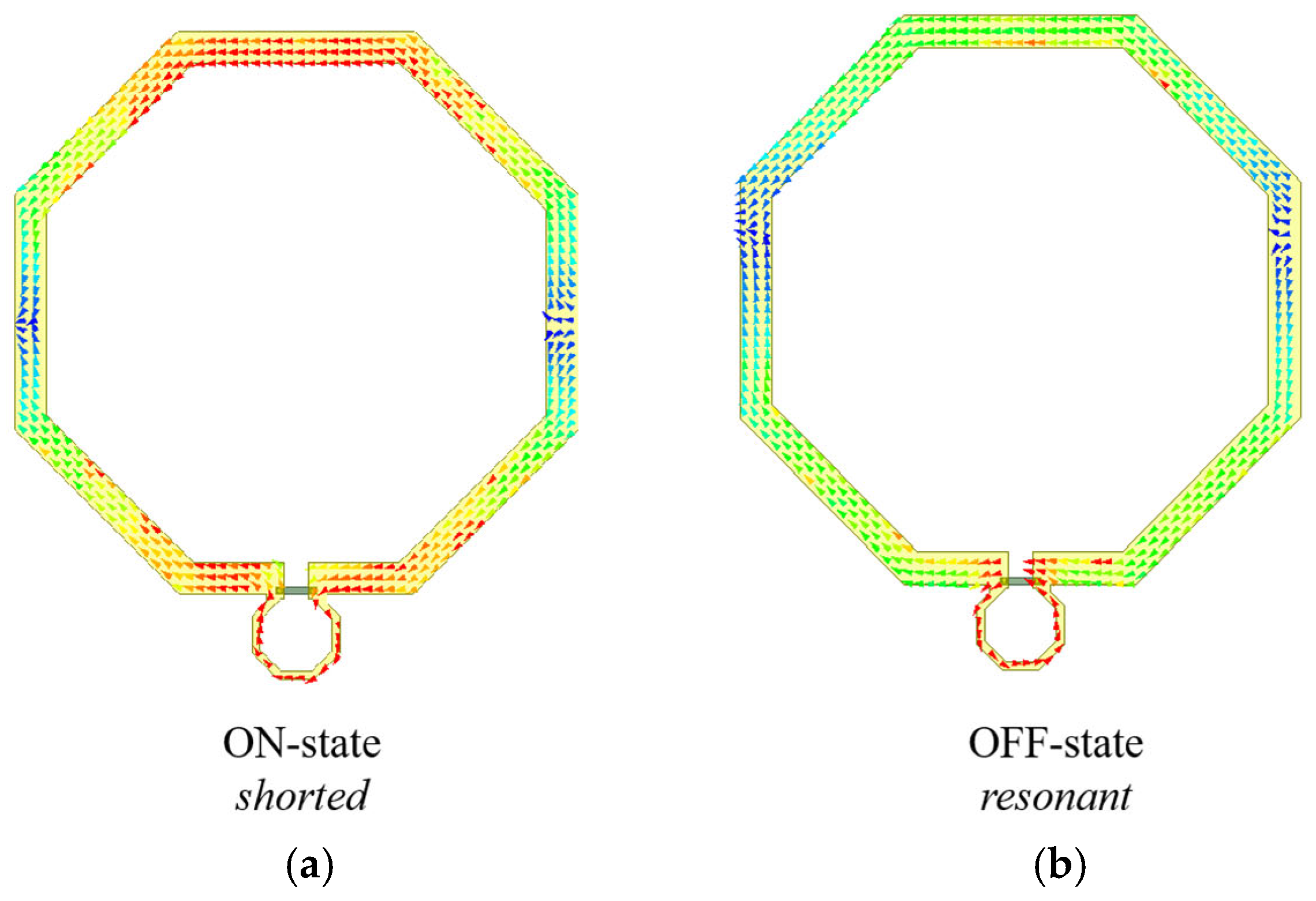
3.2.3. RRA Element Operation Principle and Simulation Results

The surface current distribution of the element under different switch states is shown in Figure 7, illustrating the working principle of the split-ring RRA element. The horizontally polarized electromagnetic wave is normally an incident for exciting the RRA element. In the ON state of the switch, horizontal surface currents are successfully excited on the split-ring structure. The currents smoothly pass through the switch, which acts as a short circuit, enabling the element to exhibit two λ₀/2 resonant modes. In the OFF state of the switch, the current in the entire loop decreases significantly. The two current null points on the loop move closer to each other, thereby reducing the resonant length. Since the effective resonant length in the ON state becomes longer than that in the OFF state, the element exhibits a lower resonant frequency in the ON state compared to the OFF state.
The simulation results shown in Figure 8 validate this operational principle. It can be observed that the resonance frequency of the element changes with the switching state: when the switch is in the ON state, the resonance frequency is 271 GHz; when the switch is in the OFF-state, the resonance frequency increases to 290 GHz. The amplitude-control RRA element exhibits an amplitude response of −4.3 dB in the ON state and −17.0 dB in the OFF state at 290 GHz.

4. Experimental Verification

To validate the performance of the terahertz amplitude-control RRA element, the split-ring resonator structure of the element is fabricated into an array employing the standard 65 nm CMOS processes, followed by tape-out, interconnects, and packaging, to construct a terahertz on-chip amplitude-control RRA prototype. Unit-level performance characterization is conducted on the prototype to extract its amplitude and phase response characteristics.

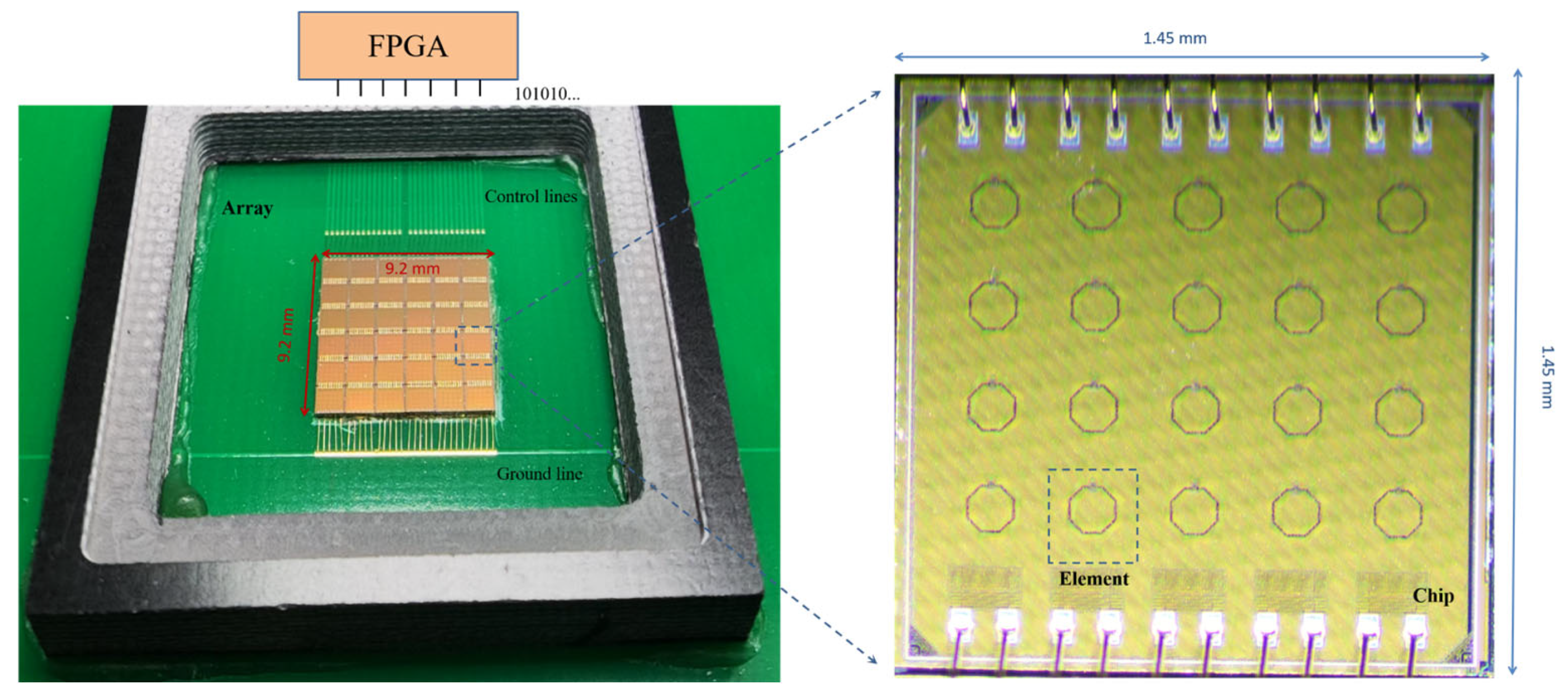
4.1. Antenna Prototype

As illustrated in Figure 9, the prototype consists of a 6 × 6 array of chip sub-arrays, with each sub-array comprising 4 × 5 unit cells. To protect the internal switches from electrostatic breakdown, electrostatic discharge (ESD) protection modules are integrated into the bonding pads located on the lower side of each sub-array. The sub-arrays measure 1.45 mm × 1.45 mm in size, with an element period of 0.26 mm. The spacing between adjacent chip sub-arrays is set to one element period, resulting in an overall phased electromagnetic surface antenna size of 10 mm × 10 mm.
The control methodology for the array adopts a column-wise addressing scheme. Specifically, the gate voltages for the switches in the 30 columns of elements are routed through bonding jumpers to the bonding pads on the upper section of the PCB, enabling external control. Meanwhile, the Direct Current (DC) ground lines for all switches are uniformly connected via bonding jumpers to the lower bonding pads on the PCB.

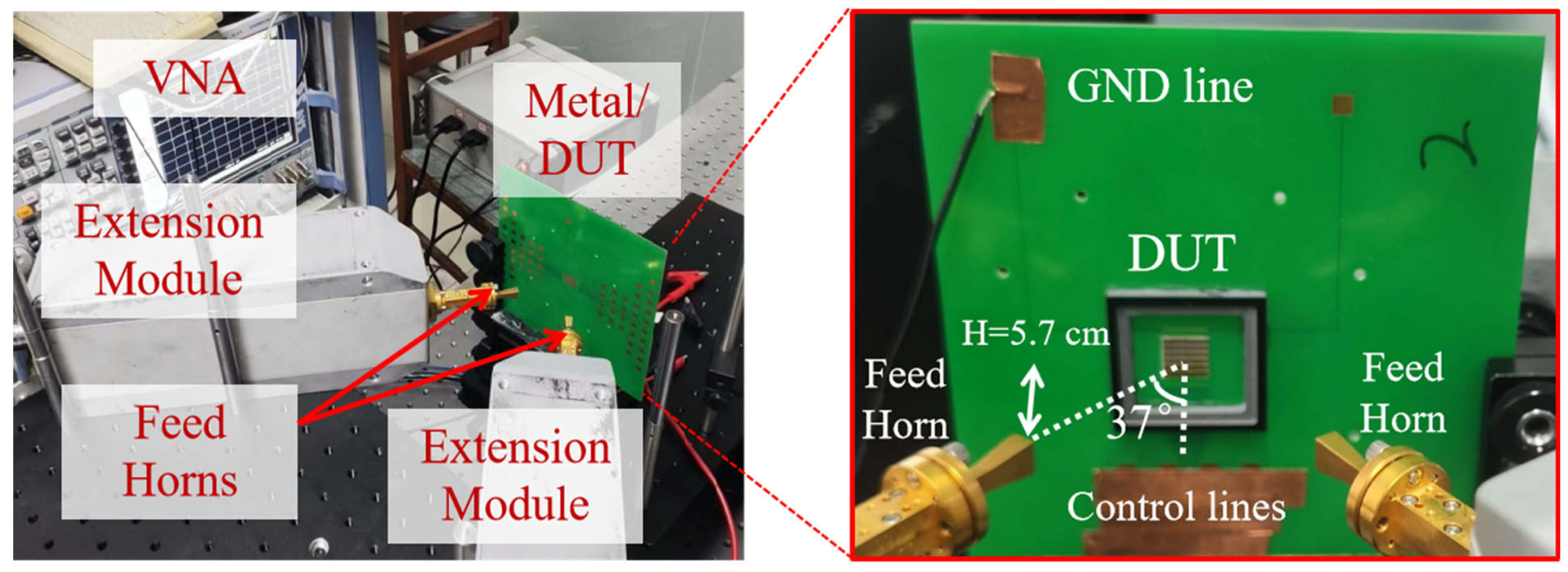
4.2. Measurement Setup and Test Results

The measurement setup for element performance testing is shown in Figure 10. The excitation feed horn illuminates the RRA or a metal plate at a 37° oblique incidence angle, while the receiving feed horn captures the terahertz waves at the same angle. The vertical distance H between the feed sources and the RRA plane is valued as 5.7 cm. By comparing the amplitude differences between the RRA and the metal plate, the element loss of the RRA can be determined.
The test results are shown in Figure 11. At 290 GHz, the RRA exhibits an amplitude of −5 dB with all switches in the ON state and −8 dB with switches in the OFF state, revealing a 3 dB amplitude control capability.
The RRA prototype successfully demonstrates amplitude control capability and low-loss performance within the target terahertz frequency range of 250–300 GHz. Experimental results not only validated the effectiveness of the terahertz switch but also confirmed the design concept. Although there were discrepancies in amplitude between the array test results and simulation results of the element, these differences were primarily due to interconnected jumpers and pads occupying too much space in the array, resulting in a fill factor of only 60.5%. This means that 39.5% of the array space was actually composed of the metal ground on the chip backside and the silicon substrate. These issues resulted in the energy from the feed horn being transmitted to the receiving horn through mirror reflection in the experiment. Consequently, the amplitude of terahertz waves in the experiments was higher than in simulations.
To validate the influence of mirror reflection on test results, the numerical calculations can be employed to demonstrate their feasibility. Specifically, we model each center of an element as an equivalent Huygens source, where the amplitude is equal to the incident feed source amplitude minus the element losses. For positions without elements, the Huygens source amplitude is equal to the incident feed source amplitude. The calculation results are shown in Figure 11.
Both test results and simulation results show an amplitude control performance of approximately 3 dB. The test results’ amplitude is lower than the simulation results because the loss of the silicon medium in the mirror reflection area was not accounted for. Thus, there is good agreement between the test results and the calculated results, which implies that improving the element fill factor can make the array test results closer to the element simulation results. We will optimize the size of the bonding pad in future designs to minimize the unoccupied space between arrays and enhance the overall performance of the RRA prototype.

4.3. Comparison and Discussion

In order to demonstrate the advantages of the proposed amplitude-control RRA, it is compared with other published works in terms of element performance in Table 3. The proposed element enables terahertz amplitude control, whereas previous studies [14,15,16,17] focused on phase/frequency shift implementations. Featuring a single-switch topology, this work minimizes THz energy loss in switches while simplifying the theoretical analysis and extending low-frequency design methodologies to THz frequencies. The measured results of the proposed element demonstrate the lowest insertion loss among [14,15,16,17]. Based on this topology, further optimization is expected to achieve better amplitude control performance for CMOS-based RRAs in THz applications.

5. Conclusions

This work presents a CMOS-based reconfigurable reflectarray element designed for terahertz (THz) applications. A custom-designed inductive loop is employed in the THz switch to resonate with parasitic capacitance. Through probe testing, TRL calibration, and parameter extraction, the switch’s equivalent impedance is obtained for the element design. By using a single switch, the proposed split-ring element design achieves low-loss amplitude control. A 30 × 24-element prototype is fabricated and tested. The test results demonstrate an amplitude difference of 3 dB at 290 GHz. The study validates the feasibility of applying low-frequency RRA design principles to THz regimes using CMOS technology, offering a scalable, low-cost pathway for future high-performance THz beam-steering systems.

Author Contributions

Conceptualization, F.Y. and S.X.; validation, Y.R. and M.L., writing and methodology, Y.W.; review and editing, F.Y. and Y.R. All authors have read and agreed to the published version of the manuscript.

Funding

This work is supported by the National Key Research and Development Program of China under Grant No. 2023YFB2905000.

Institutional Review Board Statement

Not applicable.

Informed Consent Statement

Not applicable.

Data Availability Statement

The original contributions presented in this study are included in the article. Further inquiries can be directed to the corresponding author.

Acknowledgments

We thank Guo Cheng for assistance in the probe test.

Conflicts of Interest

The authors declare no conflicts of interest.

Abbreviations

The following abbreviations are used in this manuscript:
RRAReconfigurable Refelctarray Antenna
CMOSComplementary Metal-Oxide-Semiconductor
THzTerahertz
HEMTHigh Electron Mobility Transistor
MEMSMicro-Electro-Mechanical Systems
RTAReconfigurable Transmitarray Antenna
FinFETFin Field-Effect Transistor
TRLThru-Reflect-Line
NMOSN-channel Metal-Oxide-Semiconductor
PCBPrinted Circuit Board
DCDirect Current
GSGGround–Signal–Ground
ESDElectrostatic Discharge

References

  1. Lan, F.; Wang, L.; Zeng, H.; Liang, S.; Song, T.; Liu, W.; Mazumder, P.; Yang, Z.; Zhang, Y.; Mittleman, D.M. Real-Time Programmable Metasurface for Terahertz Multifunctional Wave Front Engineering. Light Sci. Appl. 2023, 12, 191. [Google Scholar] [CrossRef] [PubMed]
  2. Malevich, Y.; Ergoktas, M.S.; Bakan, G.; Steiner, P.; Kocabas, C. Video-Speed Graphene Modulator Arrays for Terahertz Imaging Applications. ACS Photonics 2020, 7, 2374–2380. [Google Scholar] [CrossRef]
  3. Zhao, Y.; Wang, L.; Zhang, Y.; Qiao, S.; Liang, S.; Zhou, T.; Zhang, X.; Guo, X.; Feng, Z.; Lan, F.; et al. High-Speed Efficient Terahertz Modulation Based on Tunable Collective-Individual State Conversion within an Active 3 Nm Two-Dimensional Electron Gas Metasurface. Nano Lett. 2019, 19, 7588–7597. [Google Scholar] [CrossRef] [PubMed]
  4. Sensale-Rodriguez, B.; Rafique, S.; Yan, R.; Zhu, M.; Protasenko, V.; Jena, D.; Liu, L.; Xing, H.G. Terahertz Imaging Employing Graphene Modulator Arrays. Opt. Express 2013, 21, 2324. [Google Scholar] [CrossRef]
  5. Rasilainen, K.; Phan, T.D.; Berg, M.; Pärssinen, A.; Soh, P.J. Hardware Aspects of Sub-THz Antennas and Reconfigurable Intelligent Surfaces for 6G Communications. IEEE J. Sel. Areas Commun. 2023, 41, 2530–2546. [Google Scholar] [CrossRef]
  6. Wang, Y.; Zhu, K.; Xiao, Y.; Sun, H.; Li, S. A Cassegrain Antenna Design for Terahertz Focal Plane Imaging System. In Proceedings of the 2021 International Applied Computational Electromagnetics Society (ACES-China) Symposium, Chengdu, China, 28 July 2021; IEEE: Piscataway, NJ, USA, 2021; pp. 1–2. [Google Scholar]
  7. Elkhouly, M.; Holyoak, M.J.; Hendry, D.; Zierdt, M.; Singh, A.; Sayginer, M.; Shahramian, S.; Baeyens, Y. D-Band Phased-Array TX and RX Front Ends Utilizing Radio-on-Glass Technology. In Proceedings of the 2020 IEEE Radio Frequency Integrated Circuits Symposium (RFIC), Los Angeles, CA, USA, 4–6 August 2020; IEEE: Piscataway, NJ, USA, 2020; pp. 91–94. [Google Scholar]
  8. Ahmed, A.; Li, L.; Jung, M.; Rebeiz, G.M. A 140 GHz Scalable On-Grid 8×8-Element Transmit-Receive Phased-Array with Up/Down Converters and 64QAM/24 Gbps Data Rates. In Proceedings of the 2023 IEEE Radio Frequency Integrated Circuits Symposium (RFIC), San Diego, CA, USA, 11 June 2023; IEEE: Piscataway, NJ, USA, 2023; pp. 93–96. [Google Scholar]
  9. Kang, C.; Seo, J.; Jang, I.; Chung, H. Adjoint Method-Based Fourier Neural Operator Surrogate Solver for Wavefront Shaping in Tunable Metasurfaces. iScience 2025, 28, 111545. [Google Scholar] [CrossRef]
  10. Wang, Y.; Cui, D.; Wang, Y.; Yang, G.; Zhang, B.; Zhang, Y.; Wang, C. All-Solid-State Terahertz Phased Array Based on Graphene Metasurface for Ultra-Wide-Angle Beam Steering. J. Light. Technol. 2022, 40, 3814–3822. [Google Scholar] [CrossRef]
  11. Li, W.; Chen, B.; Hu, X.; Guo, H.; Wang, S.; Wu, J.; Fan, K.; Zhang, C.; Wang, H.; Jin, B.; et al. Modulo-Addition Operation Enables Terahertz Programmable Metasurface for High-Resolution Two-Dimensional Beam Steering. Sci. Adv. 2023, 9, eadi7565. [Google Scholar] [CrossRef]
  12. Zhang, Y.; Zhao, Y.; Liang, S.; Zhang, B.; Wang, L.; Zhou, T.; Kou, W.; Lan, F.; Zeng, H.; Han, J.; et al. Large Phase Modulation of THz Wave via an Enhanced Resonant Active HEMT Metasurface. Nanophotonics 2018, 8, 153–170. [Google Scholar] [CrossRef]
  13. Wu, J.; Shen, Z.; Ge, S.; Chen, B.; Shen, Z.; Wang, T.; Zhang, C.; Hu, W.; Fan, K.; Padilla, W.; et al. Liquid Crystal Programmable Metasurface for Terahertz Beam Steering. Appl. Phys. Lett. 2020, 116, 131104. [Google Scholar] [CrossRef]
  14. Liu, Y.; Sun, T.; Xu, Y.; Wu, X.; Bai, Z.; Sun, Y.; Li, H.; Zhang, H.; Chen, K.; Ruan, C.; et al. Active Tunable THz Metamaterial Array Implemented in CMOS Technology. J. Phys. D Appl. Phys. 2021, 54, 085107. [Google Scholar] [CrossRef]
  15. Venkatesh, S.; Lu, X.; Saeidi, H.; Sengupta, K. A High-Speed Programmable and Scalable Terahertz Holographic Metasurface Based on Tiled CMOS Chips. Nat. Electron. 2020, 3, 785–793. [Google Scholar] [CrossRef]
  16. Monroe, N.M.; Dogiamis, G.C.; Stingel, R.; Myers, P.; Chen, X.; Han, R. Electronic THz Pencil Beam Forming and 2D Steering for High Angular-Resolution Operation: A 98 × 98-Unit 265GHz CMOS Reflectarray with In-Unit Digital Beam Shaping and Squint Correction. In Proceedings of the 2022 IEEE International Solid- State Circuits Conference (ISSCC), San Francisco, CA, USA, 20 February 2022; IEEE: Piscataway, NJ, USA, 2022; pp. 1–3. [Google Scholar]
  17. Chen, X.; Monroe, N.M.; Dogiamis, G.C.; Stingel, R.A.; Myers, P.; Han, R. A 265-GHz CMOS Reflectarray with 98×98 Elements for 1°-Wide Beam Forming and High-Angular-Resolution Radar Imaging. IEEE J. Solid-State Circuits 2024, 59, 3655–3669. [Google Scholar] [CrossRef]
  18. Nie, X.; Hu, T.; Lan, F.; Yang, M.; Song, T.; Zhang, Y.; Yang, Z. Dual-Layer Coupling Enhanced Complementary Metasurfaces for 1-Bit Terahertz Beam Steering. In Proceedings of the 2024 International Applied Computational Electromagnetics Society Symposium (ACES-China), Xi’an, China, 16 August 2024; IEEE: Piscataway, NJ, USA, 2024; pp. 1–3. [Google Scholar]
  19. Shen, D.; Lan, F.; Wang, L.; Song, T.; Yang, M.; Hu, T.; Li, Y.; Nie, X.; Yang, J.; Liang, S.; et al. Sub-Terahertz Transmissive Reconfigurable Intelligent Surface for Integrated Beam Steering and Self-OOK-Modulation. Light Sci. Appl. 2025, 14, 13. [Google Scholar] [CrossRef]
  20. Pan, X.; Yang, F.; Liu, F.; Jiang, C.; Xu, S. A 220GHz Reconfigurable Reflectarray Antenna Using GaN HEMT Device. IEEE Trans. Terahertz Sci. Technol. 2025, 1–11. [Google Scholar] [CrossRef]
  21. Song, T.; Lan, F.; Wang, L.; Zeng, H.; Liang, S.; Yang, M.; Shen, D.; Liu, W.; Jin, S.; Zhu, Z.; et al. Terahertz Coding Metasurface with Low-Switch-Ratio for Rapid 1-Bit Phase Modulation and Beam Steering. ACS Photonics 2025, 12, 952–962. [Google Scholar] [CrossRef]
  22. Song, T.; Lan, F.; Wang, L.; Zeng, H.; Liang, S.; Yang, M.; Shen, D.; Liu, W.; Mazumder, P.; Zhang, Y.; et al. Programmable Beam Steering and Quasi-Continuous Phase Shift on a 2-Bit Terahertz Coding Metasurface with HEMT-Switched Multimodal Modulation. Opt. Express 2025, 33, 2980. [Google Scholar] [CrossRef]
  23. Liu, Z.; Guo, L.; Zhang, Q. Analytical Method for Designing Tunable Terahertz Absorbers with the Desired Frequency and Bandwidth. Opt. Express 2021, 29, 39777. [Google Scholar] [CrossRef]
  24. Zhao, F.; Xu, J.; Song, Z. Terahertz Multiple Beam Steering Using Graphene Pancharatnam-Berry Metasurfaces. IEEE Photonics J. 2022, 14, 1–6. [Google Scholar] [CrossRef]
  25. Sharma, A.; Vishwakarma, D.K. Beam Steering of Graphene-Based Terahertz Antenna Array with Circular Polarization. In Proceedings of the 2023 IEEE 7th Conference on Information and Communication Technology (CICT), Jabalpur, India, 15 December 2023; IEEE: Piscataway, NJ, USA, 2023; pp. 1–3. [Google Scholar]
  26. Liu, Z.; Guo, L.; Zhang, Q. Analytical Modeling of Terahertz Graphene Metasurfaces. Results Phys. 2024, 57, 107334. [Google Scholar] [CrossRef]
  27. Wang, P.-Y.; Rennings, A.; Erni, D. An Electronically Beam Steering Array Based on Liquid Crystals Operating in W-Band. In Proceedings of the 2022 Fifth International Workshop on Mobile Terahertz Systems (IWMTS), Duisburg, Germany, 4 July 2022; IEEE: Piscataway, NJ, USA, 2022; pp. 1–3. [Google Scholar]
  28. Xu, L.; Li, K.; Zhang, G.; Yang, J.; Yin, Z.; Zhong, M.; Lu, H.; Deng, G.; Li, Y. Fully Electrically Driven Liquid Crystal Reconfigurable Intelligent Surface for Terahertz Beam Steering. IEEE Trans. Terahertz Sci. Technol. 2024, 14, 708–717. [Google Scholar] [CrossRef]
  29. Liu, C.X.; Yang, F.; Fu, X.J.; Wu, J.W.; Zhang, L.; Yang, J.; Cui, T.J. Programmable Manipulations of Terahertz Beams by Transmissive Digital Coding Metasurfaces Based on Liquid Crystals. Adv. Opt. Mater. 2021, 9, 2100932. [Google Scholar] [CrossRef]
  30. Fu, X.; Shi, L.; Yang, J.; Fu, Y.; Liu, C.; Wu, J.W.; Yang, F.; Bao, L.; Cui, T.J. Flexible Terahertz Beam Manipulations Based on Liquid-Crystal-Integrated Programmable Metasurfaces. ACS Appl. Mater. Interfaces 2022, 14, 22287–22294. [Google Scholar] [CrossRef]
  31. Zhao, Y.; Zhang, Y.; Shi, Q.; Liang, S.; Huang, W.; Kou, W.; Yang, Z. Dynamic Photoinduced Controlling of the Large Phase Shift of Terahertz Waves via Vanadium Dioxide Coupling Nanostructures. ACS Photonics 2018, 5, 3040–3050. [Google Scholar] [CrossRef]
  32. Wang, L.; Yang, Y.; Li, S.; Deng, L.; Hong, W.; Zhang, C.; Zhu, J.; McGloin, D. Terahertz Reconfigurable Metasurface for Dynamic Non-Diffractive Orbital Angular Momentum Beams Using Vanadium Dioxide. IEEE Photonics J. 2020, 12, 1–12. [Google Scholar] [CrossRef]
  33. Wang, W.; Lv, E.; Hou, Y.; Yang, D. Broadband Beam Steering Based on Programmable VO2 Metasurface at Terahertz Frequencies. In Proceedings of the 2022 Asia Communications and Photonics Conference (ACP), Shenzhen, China, 5 November 2022; IEEE: Piscataway, NJ, USA, 2022; pp. 50–52. [Google Scholar]
  34. Chen, B.; Wang, X.; Li, W.; Li, C.; Wang, Z.; Guo, H.; Wu, J.; Fan, K.; Zhang, C.; He, Y.; et al. Electrically Addressable Integrated Intelligent Terahertz Metasurface. Sci. Adv. 2022, 8, eadd1296. [Google Scholar] [CrossRef]
  35. Long, W.-X.; Tian, Z.; Chen, R.; Moretti, M. MEMS-Based Hybrid Mechanical-Electronic Beam Steering for THz OAM Communication Chips. In Proceedings of the 2023 IEEE International Conference on Communications Workshops (ICC Workshops), Rome, Italy, 28 May 2023; IEEE: Piscataway, NJ, USA, 2023; pp. 356–360. [Google Scholar]
  36. Sun, Z.; Liang, C.; Mei, Z.; Zhou, E.; Xie, R.; You, R.; Bian, X.; Zhao, X.; Zhao, J. A MEMS Reconfigurable Air-Spaced Metamaterial Enabled Dynamic Terahertz Beam Steering. In Proceedings of the 2024 IEEE 37th International Conference on Micro Electro Mechanical Systems (MEMS), Austin, TX, USA, 21 January 2024; IEEE: Piscataway, NJ, USA, 2024; pp. 1114–1117. [Google Scholar]
  37. Zhang, Z.; Zhang, J.W.; Wu, J.W.; Liang, J.C.; Wang, Z.X.; Cheng, Q.; Cheng, Q.S.; Cui, T.J.; Yang, H.Q.; Liu, G.B.; et al. Macromodeling of Reconfigurable Intelligent Surface Based on Microwave Network Theory. IEEE Trans. Antennas Propag. 2022, 70, 8707–8717. [Google Scholar] [CrossRef]
  38. Liu, C.; Wu, Y.; Zhou, S.; Yang, F.; Ren, Y.; Xu, S.; Li, M. A Radiation Viewpoint of Reconfigurable Reflectarray Elements: Performance Limit, Evaluation Criterion, and Design Process. IEEE Trans. Antennas Propag. 2023, 71, 7881–7891. [Google Scholar] [CrossRef]
  39. Wu, Y.; Jin, Y.; Liu, C.; Yang, F.; Xu, S.; Li, M. A THz Reconfigurable Reflectarray Element Design Based on CMOS Technique. In Proceedings of the 2024 International Symposium on Antennas and Propagation (ISAP), Incheon, Republic of Korea, 5 November 2024; IEEE: Piscataway, NJ, USA, 2024; pp. 1–2. [Google Scholar]
  40. Liu, C.; Wu, Y.; Yang, F.; Xu, S.; Li, M. Can Series or Parallel Switches Improve the Performance of Reconfigurable Reflectarray Elements? In Proceedings of the 2024 IEEE International Symposium on Antennas and Propagation and INC/USNC-URSI Radio Science Meeting (AP-S/INC-USNC-URSI), Firenze, Italy, 14 July 2024; IEEE: Piscataway, NJ, USA, 2024; pp. 1181–1182. [Google Scholar]
  41. Lai, W.-C.; Chuang, H.-R. A 40–110 GHz High-Isolation CMOS Traveling-Wave T/R Switch by Using Parallel Inductor. In Proceedings of the 2015 IEEE MTT-S International Microwave Symposium, Phoenix, AZ, USA, 17–22 May 2015; IEEE: Piscataway, NJ, USA, 2015; pp. 1–3. [Google Scholar]
  42. Wu, W.; Liu, B.; He, P.; Wen, X.; Yang, H.; Cao, Y.; Wang, Z.; Shi, G.; Yang, Q.; Zhang, A.; et al. A W-Band GSG Probe Fabricated by Metal Additive Manufacturing. IEEE Trans. Instrum. Meas. 2022, 71, 1–10. [Google Scholar] [CrossRef]
Figure 1. Model and microwave network equivalence of the single-switch RRA element. (a) Model of the element. (b) Network equivalence of the single-switch element.
Applsci 15 06638 g001
Figure 2. Circuit schematic of the THz switch and small signal model of transistor employed in the switch.
Applsci 15 06638 g002
Figure 3. Switch test and TRL calibration.
Applsci 15 06638 g003
Figure 4. The single port equivalent circuit model of the THz switch.
Applsci 15 06638 g004
Figure 5. Comparison between the measured and fitted insertion loss of the switch with inductive loop.
Applsci 15 06638 g005
Figure 6. Element of the amplitude-control RRA in 3D view.
Applsci 15 06638 g006
Figure 7. Simulated current distribution of the RRA element at 290 GHz (a) ON-state and (b) OFF-state.
Applsci 15 06638 g007
Figure 8. Simulated amplitude of the RRA element.
Applsci 15 06638 g008
Figure 9. RRA and element chip tile structure.
Applsci 15 06638 g009
Figure 10. Measurement setups for the element performance.
Applsci 15 06638 g010
Figure 11. Measured and calculated amplitude change in the proposed amplitude-control RRA and the simulation results of the RRA element.
Applsci 15 06638 g011
Table 1. Equivalent parameters of the switch.
ParametersValue
L15.95 pH
Leq1.37 pH
OFF-stateRoff198.7 Ω
Coff16.61 fF
ON-stateRon48.6 Ω
Con12.29 fF
Table 2. Impedance parameters of the two-port network.
ParametersValue
Z1191.57 − 290.08 × i Ω
Z1220.86 − 67.60 × i Ω
Z2120.86 − 67.60 × i Ω
Z228.26 + 48.86 × i Ω
η0377 Ω
Table 3. Element performance comparison for CMOS-based RRA in THz frequency band.
Ref.TechnologyFrequencySwitch NumberElement TypeElement Loss
[14]180 nm300 GHz1Transmit/
Frequency shift
15 dB
(Δφ = 4°)
[15]65 nm300 GHz8Transmit/
Phase shift
5~30 dB
(* Δφ = 240°)
[17]22 nm265 GHz2Reflect/
Phase shift
14.7 dB
(Δφ = 180°)
This Work65 nm290 GHz1Reflect/
Amplitude control
5~8 dB
* Simulated results.
Disclaimer/Publisher’s Note: The statements, opinions and data contained in all publications are solely those of the individual author(s) and contributor(s) and not of MDPI and/or the editor(s). MDPI and/or the editor(s) disclaim responsibility for any injury to people or property resulting from any ideas, methods, instructions or products referred to in the content.

