Article

Bessel Picosecond Laser Cutting Glass-Ceramics: Optimization of Processing Point Spacing, Incident Power, and Burst Mode

1
Zhongshan Branch of State Key Laboratory of Electronic Thin Films and Integrated Devices, Zhongshan Institute, College of Electronic and Information, University of Electronic Science and Technology of China, Zhongshan 528402, China
2
Shenzhen Key Laboratory of Micro/Nano Photonics and Information Technology, Optoelectronic Devices and Systems, College of Physics and Optoelectronic Engineering, Ministry of Education/Guangdong Province, State Key Lab Radio F, Shenzhen University, Shenzhen 518060, China
*
Author to whom correspondence should be addressed.
Appl. Sci. 2025, 15(11), 6172; https://doi.org/10.3390/app15116172
Submission received: 16 February 2025 / Revised: 13 May 2025 / Accepted: 27 May 2025 / Published: 30 May 2025

Abstract

Recent advances in glass-ceramics research have expanded their applications in astronomy, optoelectronics, and laser systems. However, precision cutting technology remains challenging. This study optimized picosecond laser processing parameters for 600 nm-thick glass-ceramics, revealing critical influences of point spacing, laser energy, and pulse number. Atomic force microscopy showed that 1 µm processing spacing enabled uniform ablation grooves with optimal roughness. Two-pulse configurations achieved the most consistent surface improvement. At 12.5 W incident power, samples exhibited minimized average roughness (219 nm) with localized values reaching 208 nm, alongside 1.2 N breaking stress.

1. Introduction

Glass-ceramics [1,2,3,4,5] represent an innovative substance that combines a specific amount of crystalline structure with leftover glassy material, resulting from the thermal processing of base glass. This material exhibits properties such as transparency to visible light, robust mechanical durability, and the ability to modify its thermal expansion rate. It is widely utilized in various sectors, including aerospace, electronics, machinery, chemical manufacturing, laser technology, and more [6,7,8]. Looking ahead, it is anticipated to continue being a focal point in the realm of materials science and engineering for an extended duration. Hard and brittle properties are one of the characteristics of microcrystalline glass, and there are still some problems with its processing. When hard and brittle materials are processed using conventional metalworking techniques [9], the workpiece is susceptible to fracture. For instance, during diamond blade cutting, the blade’s direct contact with the wafer can result in issues such as splash residue, surface damage, tool wear, microcracks, and residual stress [10]. These issues can potentially lead to product defects. Additionally, these methods often suffer from low processing efficiency, high energy consumption, suboptimal processing quality, and an inability to meet numerous design specifications. Consequently, many researchers are investigating efficient and high-quality methods for processing hard and brittle materials [11].
In recent years, ultra-short pulse lasers [12,13] have emerged as a prominent research focus in the machining field due to their high precision, non-contact operation, and high energy density. Pulsed lasers utilizing Bessel beams [14,15,16,17,18] have found extensive application in the micro- and nano-processing of hard and brittle materials. Studies have validated the beneficial impact of laser space-time shaping on the processing of glass materials. Research indicates that processing parameters, including image point spacing, laser incident power, and pulse mode, significantly influence the quality of fiber processing [19,20,21,22,23]. Many experts concur that the roughness of the sample cross-section serves as a critical indicator of laser cutting quality [24,25]. Hoyo et al. [26] investigated nanoscale energy deposition in glass using dual ultrafine Bessel pulses; however, they did not examine the effect of pulse count on glass processing. Chen and Liao et al. [27,28] employed ultrafine laser Bessel beams for cutting both glass and sapphire, optimizing energy deposition to minimize the heat-affected zone and enhance the sidewall quality of the cut specimens; nevertheless, the influence of processing point spacing was not thoroughly explored. Wang et al. [29] utilized femtosecond laser Bessel beams to cut thin glass through internal scratches and mechanical fractures, analyzing how pulse energy and processing point spacing affected the strength and edge cross-sectional morphology of samples, although surface roughness was not addressed in their study. Liao and Jiang et al. [27,30] examined the effects of laser incident power, processing point spacing, and defocusing distance on quartz glass.
This study takes the picosecond pulsed laser cutting of microcrystalline glass as the object of re-study and uses Bessel beams to conduct experiments, utilizing the roughness of the separation surface and the mechanical stress required for the separation, quantitatively analyzing the influence of laser power, processing spacing, and pulse train mode on the laser cutting effect, systematically investigating the influence of different ultra-fast laser processing parameters on the quality of hard and brittle material processing under the processing condition using the Bessel beam, and providing a reference for the precise control process of pulsed laser cutting of microcrystalline glass. The effects of different ultrafast laser processing parameters on the quality of hard and brittle materials are systematically investigated under the condition of Bessel beam processing.

2. Test Materials

The sample employed in the experiment was an experimental glass-ceramic sheet with a thickness of 600 nm and dimensions of 50 × 50 mm. The pre-treatment size of the glass sheet prior to the experiment measured 7.5 × 5 mm, with an allowable error range of ±0.2 mm. The mechanical properties of the glass-ceramics are detailed in Table 1.

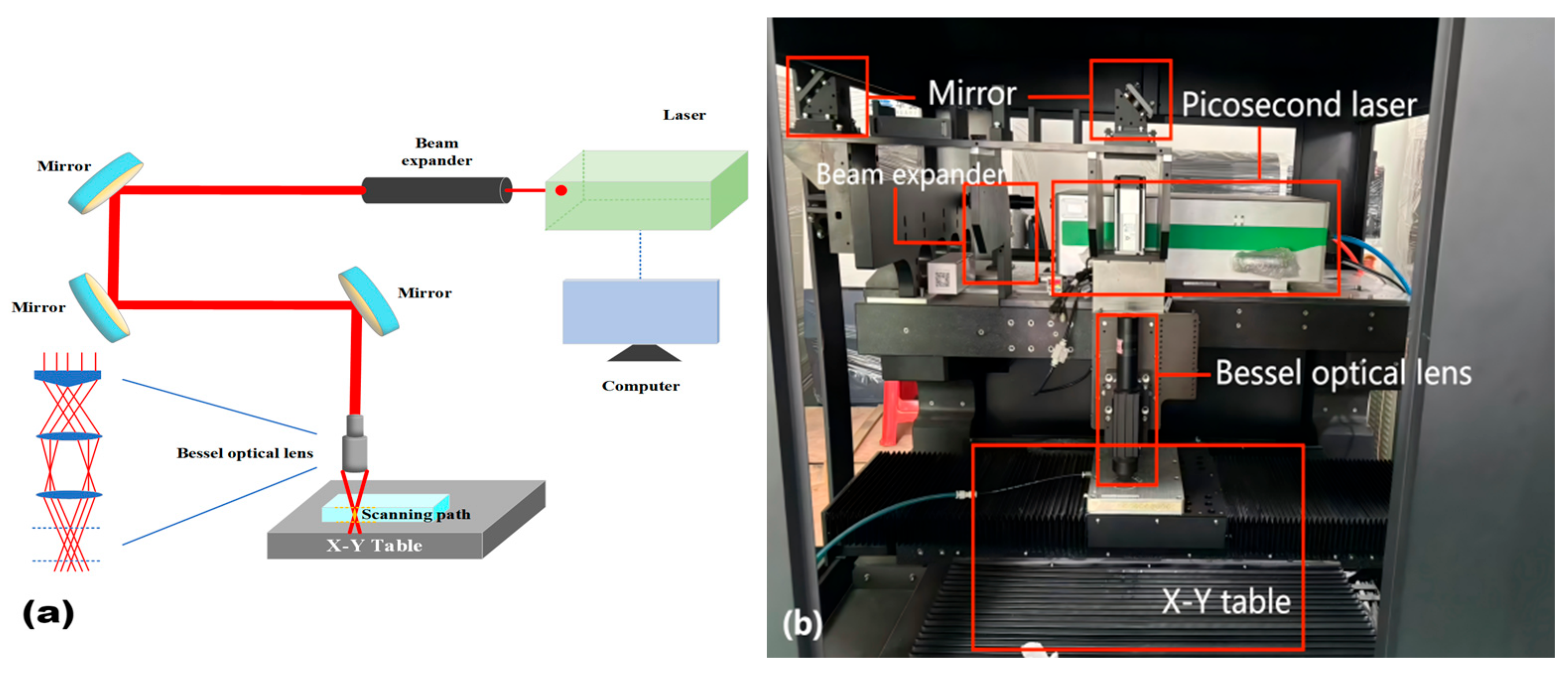
2.1. Test Instruments

In this experiment, a picosecond pulsed laser with a wavelength of 1064 nm and a fixed frequency of 100 kHz is utilized. The operational principles of the experimental system for Searle beam cutting glass-ceramics using the selected picosecond laser (YP-IR-30, Huakuai, Dongguan, China) are illustrated in Figure 1. The positioning accuracy of the 3D mobile platform (CE4550-I-PG, Huayi Laser, Dongguan, China) is ±5 µm, with a repetition accuracy of ±2 µm. The X-Y direction facilitates the planar motion of the table, whereas the Z direction controls the focal depth of the Bessel beam to encompass the entire cross-section of the sample. In Position Synchronous Output (PSO) mode, the laser can be applied at all stages along its trajectory and can perform acceleration, deceleration, and curved motions to achieve uniform pulse energy irradiation across the processed object. The burst mode involves selecting multiple sub-pulses that share the same repetition rate as that of the seed source through a controllable optical switch to generate a pulse train output.
The cutting section and the top ablation hole of the glass-ceramics were examined using a metallographic microscope (BX51M, OLYMPUS, Tokyo, Japan). The local morphology of the glass cross-section was characterized through scanning electron microscopy (SEM-VEGA3, TESCAN, Brno, Czech Republic). The surface morphology and roughness of the cross-section were assessed with an atomic force microscope (AFM-DSM14049BF1, Bruker, Billerica, MA, USA). The fracture strength at the cutting point of the glass-ceramics was measured using a pointer-type push tension meter (NK-50, AIGU, Dongguan, China). The relevant parameter table of the processing system is shown in Table 2.

2.2. Test and Analysis Methods
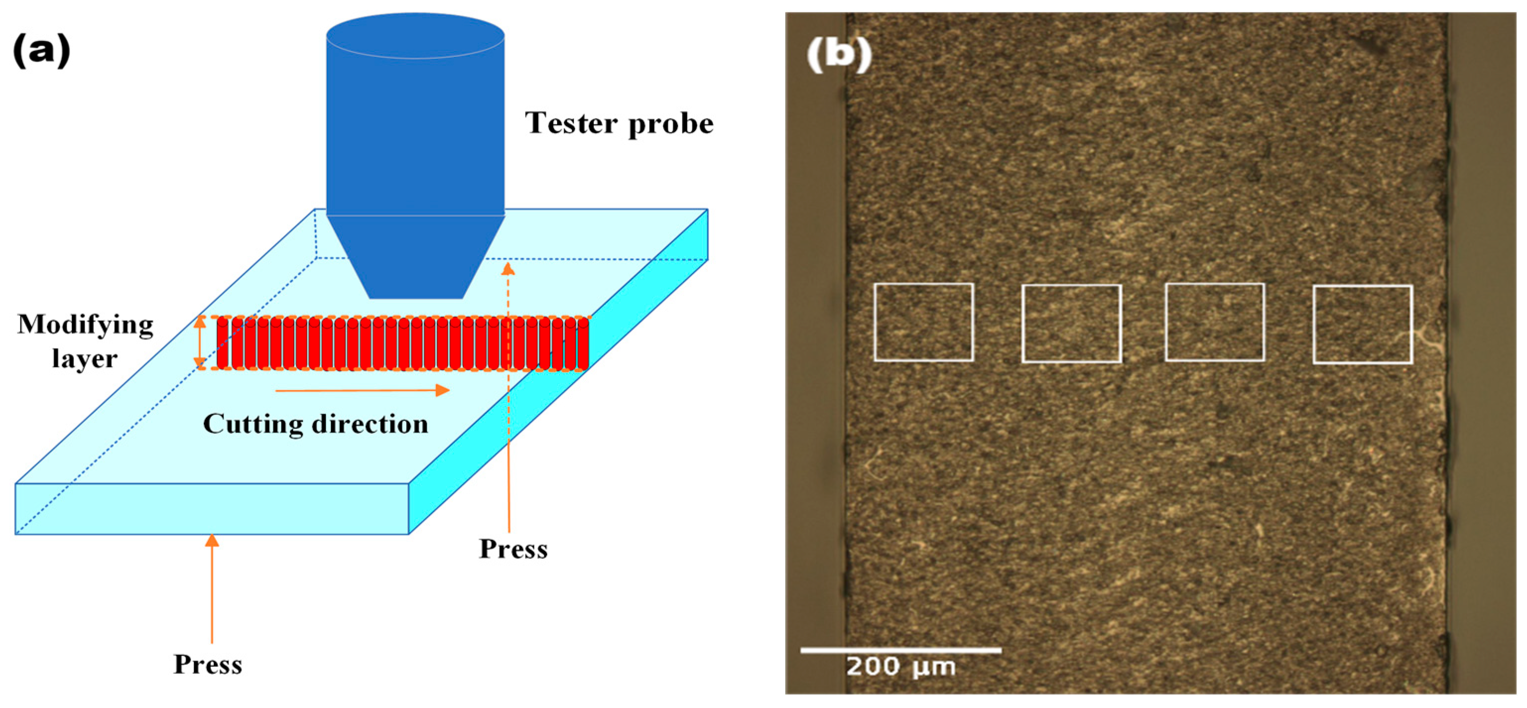
2.2.1. Test Methods

The laser generated by the picosecond laser passes through a telephoto lens to produce a Bessel beam, which is characterized by its extended focusing depth of approximately 1 mm. By adjusting the Z-axis of the cutting platform, the beam can be focused to cover the sample section effectively. This focused beam is then utilized to modify and cut into the microcrystalline glass sheet. The X-Y platform is maneuvered along a specified path, allowing for varying machining point spacings that yield different aperture shapes.
Additionally, stress was applied to both sides of the machining aperture path, as illustrated in Figure 2a, promoting crack propagation from small apertures and facilitating separation of the glass-ceramics post-cutting. The cross-section resulting from this process was subsequently examined. Given an AFM detection range of 50 × 50 µm, four repeated observations were conducted on the cross-section, with an average value calculated thereafter; this average roughness serves as an indicator of the cutting effect achieved by the Bessel beam on glass-ceramics. The results of these observations are presented in Figure 2b.

2.2.2. Analysis Method

The picosecond laser produces a Gaussian beam with a radius of 3 mm through a laser beam extension mirror and a Gaussian beam through a Bessel lens. In this paper, the basic Angle α inside the Bezier lens is selected as 5°, the axial cone refractive index n = 1.45, and the main Bezier beam cone Angle θ are calculated as follows according to equation (1):
θ = arcsin n × sin α α
The primary Bessel beam produces a secondary Bessel beam through a telescope system using a scaling factor M = 8 (4f system). The conical Angle φ, diameter D, and length l of a secondary Bessel beam are calculated by the following Equations (2)–(4):
φ = arctan tan θ × M
D = 4.8096 k sin θ
l = w 0 M tan θ
where ω0 = 3 mm is the waist radius of the incident Gaussian beam and k is the dielectric wave number. The intensity distribution of the second-order Bessel beam can be calculated by Equation (5), where is the zero order Bessel function and is the incident laser energy.
I = I 0 z l J 0 2 4.8096 r D exp 2 z 2 l 2
The zero-order Bessel beam, also referred to as a non-diffracting beam, is characterized by its perpendicular orientation to the transmission direction of the transverse light intensity distribution. This configuration features a central bright spot (main lobe) surrounded by multiple concentric rings (sidelobes). Each sidelobe carries approximately equal energy, resulting in a highly concentrated light intensity at the center of the main lobe. Notably, the transverse light intensity distribution remains invariant over non-diffracting propagation distances. In this study, Zmax (ANSYS Zemax OpticStudio 2023 R1) and MATLAB (MATLAB R2024a) were employed to simulate both the spot and intensity distribution of the Bessel beam. The central spot and surrounding interference rings collectively form what is known as a Bessel spot. Figure 3a illustrates the simulated Bessel spot generated using Zmax, while Figure 3b presents the results of intensity distribution obtained through MATLAB simulation. It can be observed that the intensity of the central main lobe is maximized, whereas the intensities of sidelobes diminish with an increase in beam diameter.

3. Results and Discussion

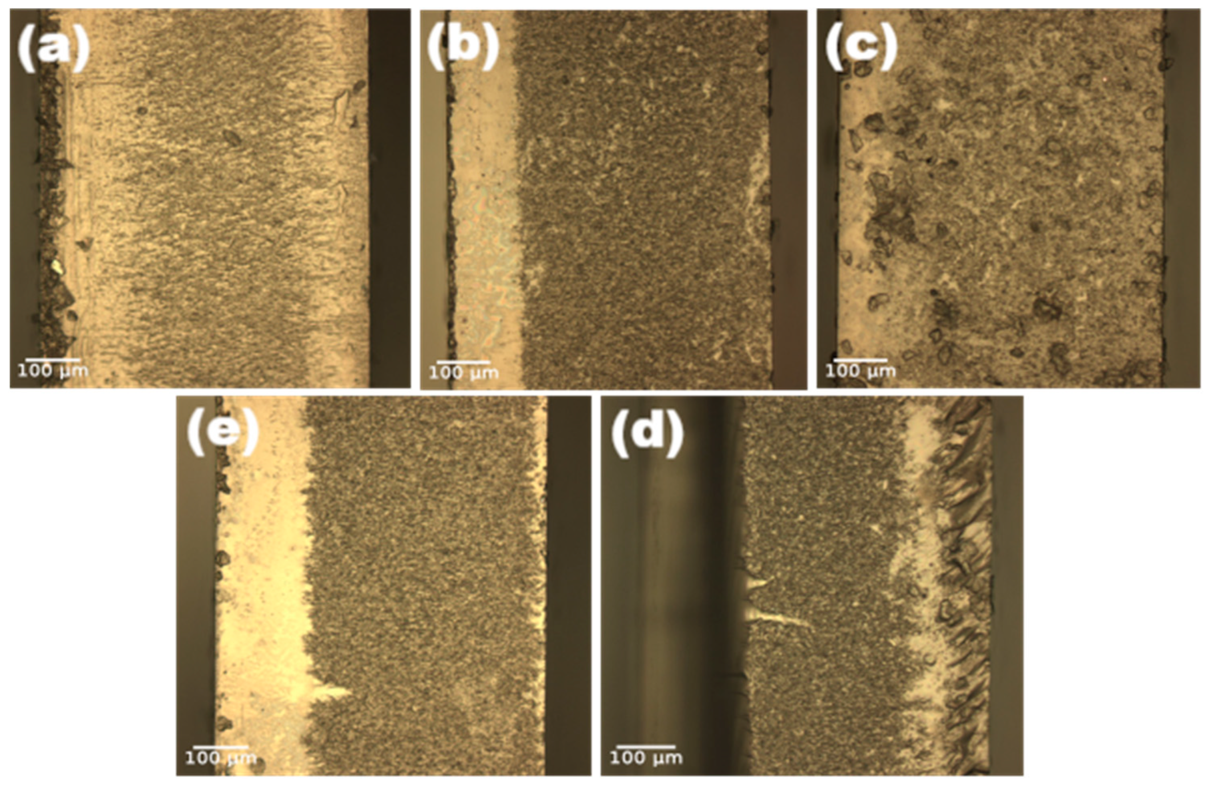
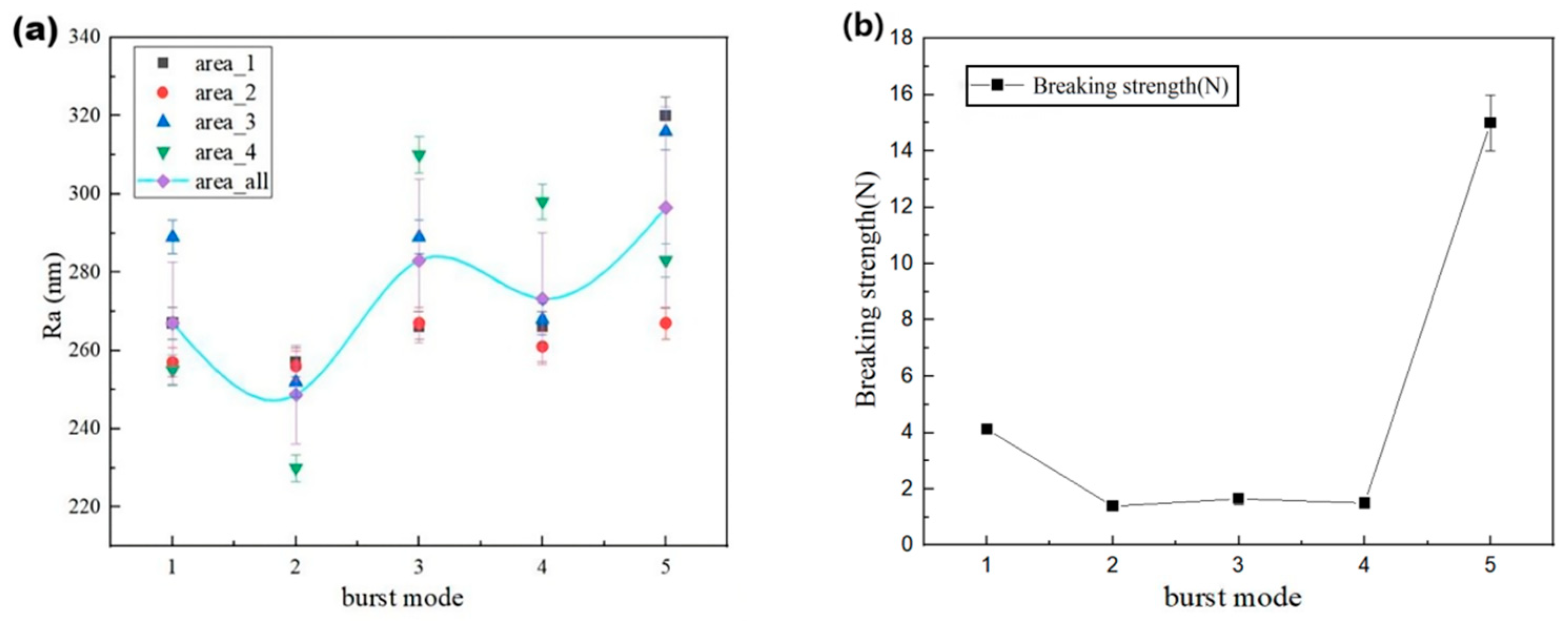
3.1. The Influence of the Number of Processing Pulses on the Cutting Effect

The samples were laser cut with 1, 2, 3, 4, and 5 pulse train patterns at a laser frequency of 100 kHz. The test results are shown in Figure 4. The concentration of energy from a single pulse results in incomplete, reforming near the upper and lower surfaces of the sample, where transition ablation can be seen on the upper surface and areas of melt sputtering can be seen after the ablation. The overall correction was observed to be the most uniform and effective when using the dual pulse string mode. This is due to the fact that the first sub-pulse in the pulse string ionizes a large number of free electrons when it reaches the surface of the sample, and the free electrons interact with the lattice to produce a good melting effect; then, when the second sub-pulse is injected, the energy is redistributed, which affects the distribution of the electron density and optimizes the melting effect of the first sub-pulse. As the number of pulse trains increases, it is clear that the unmodified area of the sample also increases, which is attributed to the fact that too many pulse trains dispersed the energy, resulting in incomplete modification of the microcrystalline glass.
Atomic force microscopy (AFM) morphology was performed on localized areas of the sample cross-section with pulse string modes of 1, 2, 3, 4, and 5, as shown in Figure 5. The local topographic analysis shows that the area of the unmodified region is larger when the pulse pattern is set to 1. In contrast, when the number of pulses was 2, the overall retexturization appeared to be the most uniform and fine. At pulse number 3, due to the decrease in energy contained in each individual pulse, a few localized untextured areas appeared, as evidenced by the increase in the height of the columns with the maximum roughness in the textured area and the appearance of lagging areas. When we further adjusted the pulse pattern to 4, these hysteretic regions expanded more in the unmodified region and the roughness risers were seen to be more concave and inconsistent; however, when the pulse pattern number was 5, the blocky risers began to appear in the unmodified region, when the roughness reached its maximum.
When the laser injection power is set at 10 W and the processing point spacing is 1 µm, the relationship between breaking strength and the number of pulses is illustrated in Figure 6b. As depicted in Figure 6b, when the pulse count reaches 2, the fracture strength of the sample is observed to be at its minimum. However, as the number of pulses continues to increase beyond this point, an enhancement in fracture strength can be noted. The trend regarding stress variation with respect to fracture mode aligns consistently with that of surface roughness. Additionally, modifications made within the correction area significantly influence both the fracture strength and roughness characteristics of the specimen section.
In summary, when the pulse number is 2, the processing effect is the best.

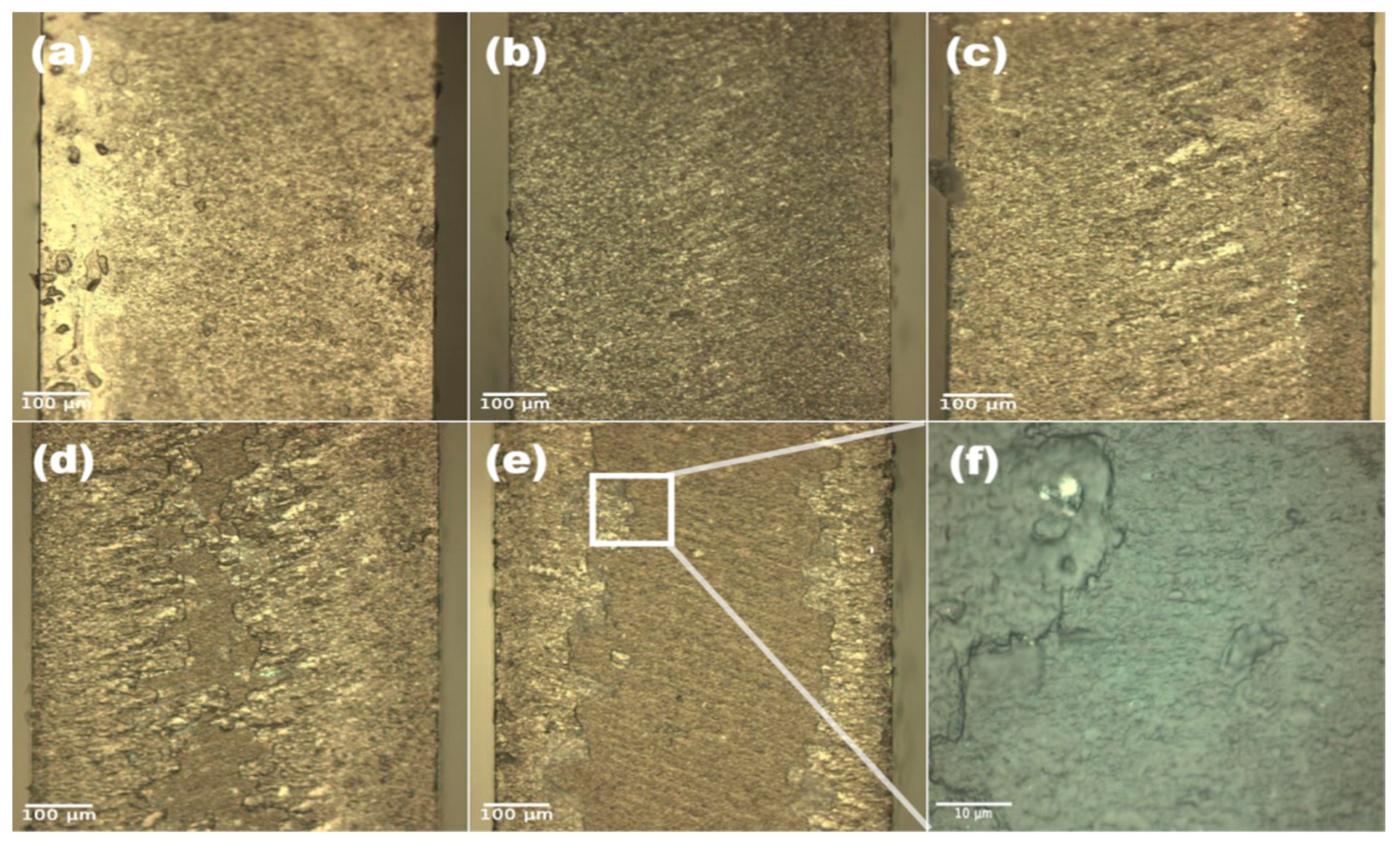
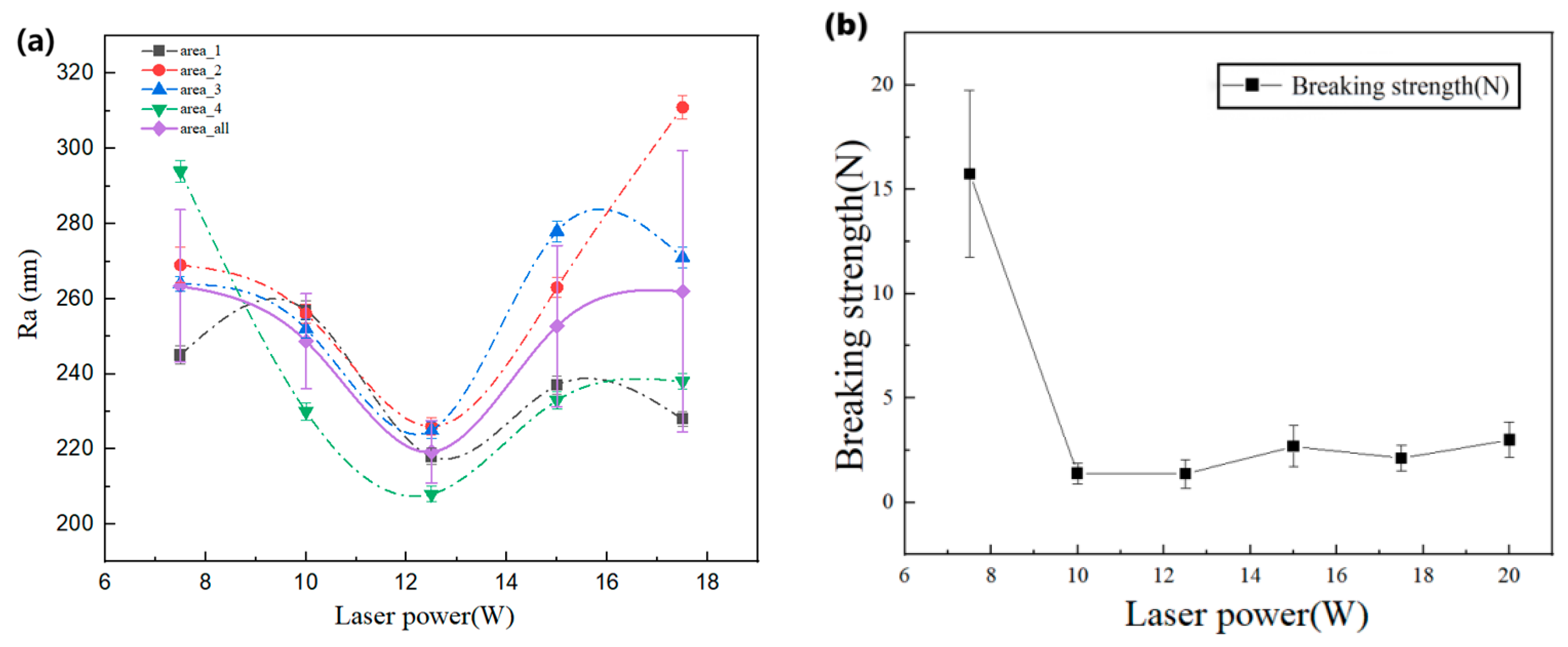
3.2. Influence of Incident Laser Power on the Cutting Effect

When the incident laser power changes, the intensity distribution of the Bessel beam will also be affected. As shown in Figure 7, when the processing point spacing is 1 µm and the number of burst modes is 2, the defocusing distance is adjusted so that the focal depth covers the entire section. When the incident laser power is too high, such as greater than 12.5 W, the Bessel beam may cause excessive crystallization of the material during sample processing. This excessive crystallization cannot improve the machining quality but may lead to increased section roughness.
The roughness of the sample section under different energies was characterized, and the results are shown in Figure 8a below. The test results of different power roughness are as follows: when the incident power is 12.5 W, the average roughness is the lowest and the ablation is the most uniform; when the incident energy is less than this value, the ablation is not uniform, and the focal depth of the Bezier beam cannot cover the whole section, resulting in high roughness; when the incident energy is greater than 12.5 W, with the increase in the incident energy, the section roughness further increases, and the section roughness uniformity decreases; and when the incident energy is greater than 15 W, the standard deviation of roughness decreases. The average roughness of the section is the lowest, and the standard deviation of the roughness decreases with the increase in the incident energy, and the standard deviation of the average roughness also increases.
This recrystallization phenomenon increases the roughness in the region where the Bezier beam energy distribution is large. In this paper, it is suggested that the local electron density changes lead to several potential changes, and the local high temperature leads to this phenomenon. As shown in Table 3, when the laser injection power is 17.5 W and 20 W, the maximum roughness difference in different regions reaches 202.05 nm and 373.3 nm, respectively. Therefore, it is assumed that with the further increase in the laser injection power, the internal crystallization will increase, resulting in a further increase in the roughness difference between different regions.
The fracture strength of laser incident power is characterized by the average roughness of the cross section and the maximum difference in each region under different incident powers in Table 3. The results are shown in Figure 8b. In Figure 8b, when the laser frequency is set to 100 kHz, the processing point spacing is 1 µm, and the laser injection power is 7.5 W; it is observed that the modification effect is incomplete and the breaking strength is greater than 20 N. With the increase in laser power, the energy of the Bessel beam increases correspondingly, and it can cover a larger modified area. When the laser injection power reaches 12.5 W, the modified layer completely covers the whole section, and the fracture strength decreases significantly. After the laser injection power is further increased, the fracture strength is stable at about 2 N, which shows the effect of high power on the modification effect.
In summary, when the laser power is 12.5 W, the best processing effect can be obtained.

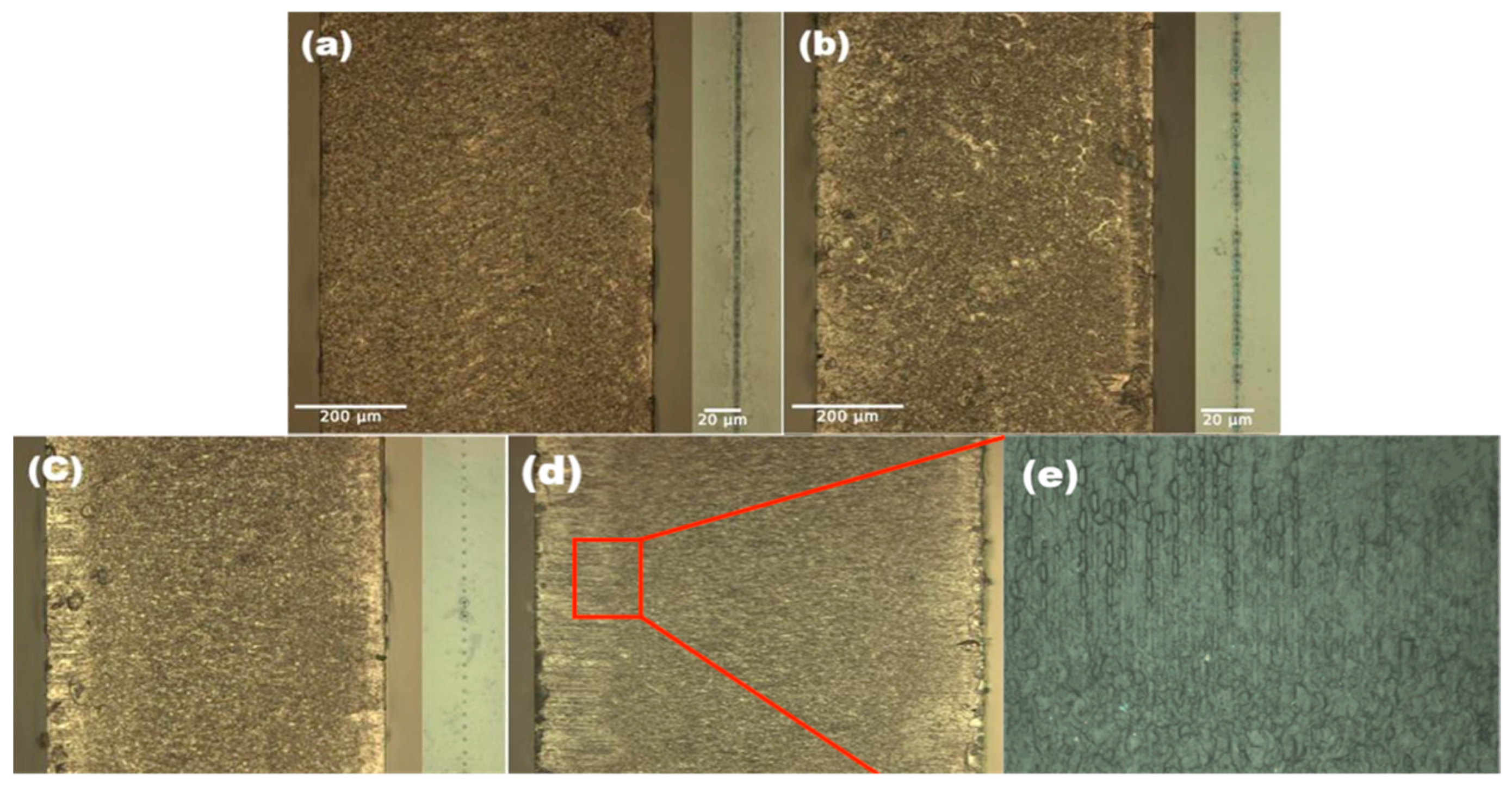
3.3. Influence of Machining Point Spacing on Cutting Quality

When the pulse repetition rate is set to 100 kHz, the incident laser frequency is at 12.5 W and the pulse mode is configured to 2; the cutting results of varying processing point spacings are illustrated in Figure 9. The laser irradiation on the linear shape of the microholes results in molten sputtering. As the processing point spacing increases, the melting area surrounding the microholes gradually decreases. At a processing point spacing of 1 µm (Figure 9a), the microholes coalesce into an ablative tank. When the processing point spacing exceeds 3 µm, the microholes become separated, with more pronounced cracks connecting them. At a spacing of 5 µm, the micropores are more widely dispersed, forming independently. This phenomenon is depicted in Figure 9c. With a treatment interval of 5 µm, the unaltered area increases, making sample separation challenging. As shown in Figure 9d, intermittent laser ablation cavities can be observed in both the upper and lower layers of the cross-section of the glass-ceramics. These cavities form micron channels with an ablative diameter of approximately 1.88 µm and a gap between channels of about 3.6 µm. Similar micron channels were observed at point spacings less than 3 µm. However, when the distance between processing points is too small, the micron channel influence regions overlap, leading to no distinct channel morphology at a point spacing of 1 µm.
The characterization of sample cross-sectional roughness generated by different machining point spacings is presented in Figure 10a. The roughness increases with increasing machining point spacing, particularly near the middle of the sample, which aligns with the variation trend of Bessel beam energy along the z-axis in this experiment. At a point spacing of 1 µm, there is minimal difference in roughness between regions. As the point spacing increases, the section area of the sample exhibits varied correction forms, resulting in greater regional roughness differences. At a point spacing of 5 µm, the average roughness difference between region 3 and region 4 reaches 130 nm.
Additionally, the fracture strength of specimens with different processing point spacings was measured using a hand press tester. The stress variation with the distance between laser processing points is shown in Figure 10b. As the point spacing increases, so does the unmodified zone area, leading to higher stress required for specimen fracture. Combining this with Figure 4, it is evident that increased point spacing results in wider micron channel spacing and larger unmodified areas within the channels, contributing to increased sample roughness. The trends in roughness and fracture strength correlate with changes in point spacing.
In summary, the optimal processing quality is achieved at a processing point spacing of 1 µm, where the overall shape remains uniform.

4. Conclusions

In this study, we innovatively combined the multi-pulse sequence mode with the Bessel beam, which can cover the whole modified cross-section with its long focal depth compared with the traditional multi-focus Gaussian beam processing. A picosecond laser cutting system was established according to the experimental requirements, and a picosecond pulsed laser (YPP-IR-30, HUAKUAI, China) with a wavelength of 1064 nm and a fixed frequency of 100 kHz was selected to cut the microcrystalline glass samples with high quality. The experimental results show that when the number of pulse sequence modes is 2, the laser power is 12.5 W, and the processing point spacing is 1 μm; the processing quality of the microcrystalline glass reaches the optimal level, the average roughness of its cross-section is reduced to 219 nm, and the mechanical stress required by the blade is only 1.2 N, which provides an important theoretical basis and a process optimization strategy for the high-precision and low-damage processing of microcrystalline glass.

Author Contributions

Conceptualization, Y.D. and Y.S.; methodology, X.P. and Y.D.; software, C.P.; validation, X.P. and J.L.; formal analysis, X.P. and J.Y.; investigation, Z.Z.; resources, Y.S.; data curation, Z.L.; writing—original draft preparation, X.P.; writing—review and editing, X.P. and Y.D.; visualization, C.D.; supervision, Q.G. and Z.Z.; project administration, Y.C.; funding acquisition, X.P. All authors have read and agreed to the published version of the manuscript.

Funding

The authors acknowledge the funding from the National Natural Science Foundation of China (62241502, 62105042); Guangdong Natural Science Foundation (2018A030310662); Key Scientific Research Project of the Department of Education of Guangdong Province (2024ZDZX3064, 2022ZDZX3040, 2023ZDZX1042); and Zhongshan Social Public Welfare Science and Basic Research Project (2023B2012).

Institutional Review Board Statement

Not applicable.

Informed Consent Statement

Not applicable.

Data Availability Statement

The original contributions presented in the study are included in the article; further inquiries can be directed to the corresponding author.

Conflicts of Interest

The authors declare no conflicts of interest.

References

  1. Deubener, J.; Allix, M.; Davis, M.J.; Duran, A.; Höche, T.; Honma, T.; Komatsu, T.; Krüger, S.; Mitra, I.; Müller, R.; et al. Updated definition of glass-ceramics. J. Non Cryst. Solids 2018, 501, 3–10. [Google Scholar] [CrossRef]
  2. Kartopu, G.; Oklobia, O.; Tansel, T.; Jones, S.; Irvine, S.J.C. A facile photolithography process enabling pinhole-free thin film photovoltaic modules on soda-lime glass. Sol. Energy Mater. Sol. Cells 2023, 251, 112112. [Google Scholar] [CrossRef]
  3. Kwon, O.; Takahashi, Y.; Miyazaki, T.; Terakado, N.; Fujiwara, T. Nanostructure and photocatalytic behavior of glass-ceramics in system. J. Ceram. Soc. Jpn. 2020, 128, 839–842. [Google Scholar] [CrossRef]
  4. Ma, Y.; Guo, C.; Meng, X.; Yang, S.; Kou, S.; Deng, J.; Fan, S.; Liu, X. Corrosion resistance and microstructural evolution of y-al-si-o glass-ceramics environmental barrier coating candidate in the presence of cmas. Mater. Charact. 2025, 220, 114685. [Google Scholar] [CrossRef]
  5. Ibrahim, S.; El-Kheshen, A.A.; Abdel-baki, M.; Fayad, A.M.; Hamdy, Y.M.; Ibrahim, M.M.; Marzouk, M.A. Synthesis and characterization of erbium silica glass and glass-ceramics for potential low-emissivity coating applications. Ceram. Int. 2025, 51, 458–472. [Google Scholar] [CrossRef]
  6. Kažukauskas, E.; Butkus, S.; Jukna, V.; Paipulas, D. Surface roughness control in deep engraving of fused silica using femtosecond laser ablation. Surf. Interfaces 2024, 50, 104471. [Google Scholar] [CrossRef]
  7. Sugioka, K.; Cheng, Y. Ultrafast lasers—Reliable tools for advanced materials processing. Light Sci. Appl. 2014, 3, e149. [Google Scholar] [CrossRef]
  8. Xiong, S.; Wang, R.; Tao, H. Ultrafast laser micromachining the ultra-low expansion glass-ceramic: Optimization of processing parameters and physical mechanism. J. Eur. Ceram. Soc. 2021, 41, 5990–5999. [Google Scholar] [CrossRef]
  9. Zhao, J.; Xu, X.; Li, W.; Hang, W. Material removal modes and processing mechanism in microultrasonic machining of ball ceramic tool. Ceram. Int. 2024, 50, 28844–28856. [Google Scholar] [CrossRef]
  10. Feng, J.; Wang, J.; Liu, H.; Sun, Y.; Fu, X.; Ji, S.; Liao, Y.; Tian, Y. A review of an investigation of the ultrafast laser processing of brittle and hard materials. Materials 2024, 17, 3657. [Google Scholar] [CrossRef]
  11. Jedrkiewicz, O.; Kumar, S.; Sotillo, B.; Bollani, M.; Chiappini, A.; Ferrari, M.; Ramponi, R.; Di Trapani, P.; Eaton, S.M. Pulsed bessel beam-induced microchannels on a diamond surface for versatile microfluidic and sensing applications. Opt. Mater. Express 2017, 7, 1962–1970. [Google Scholar] [CrossRef]
  12. Jia, X.; Vrijburg, F.; Zhang, W.; Groenendijk, M.; Pei, Y. Ultrasmooth micromilling of stainless steel by ultrashort pulsed laser ablation using mhz bursts. ACS Appl. Mater. Interfaces 2025, 17, 7989–8002. [Google Scholar] [CrossRef]
  13. Yildirim, K.; Nagarajan, B.; Tjahjowidodo, T.; Castagne, S. Review of in-situ process monitoring for ultra-short pulse laser micromanufacturing. J. Manuf. Process. 2025, 133, 1126–1159. [Google Scholar] [CrossRef]
  14. Courvoisier, F.; Zhang, J.; Bhuyan, M.K.; Jacquot, M.; Dudley, J.M. Applications of femtosecond bessel beams to laser ablation. Appl. Phys. A 2012, 112, 29–34. [Google Scholar] [CrossRef]
  15. Guilberteau, T.; Balage, P.; Lafargue, M.; Lopez, J.; Gemini, L.; Manek-Hönninger, I. Bessel beam femtosecond laser interaction with fused silica before and after chemical etching: Comparison of single pulse, mhz-burst, and ghz-burst. Micromachines 2024, 15, 1313. [Google Scholar] [CrossRef]
  16. Liang, G.; Sun, S.; Wang, J.; Qu, Z.; Wei, T.; Liu, X.; Sun, H.; Monka, P.P.; Hamza, A. Application of array bessel beam generated by superposition method in electronic glass cutting. Opt. Lasers Eng. 2024, 181, 108384. [Google Scholar] [CrossRef]
  17. Marx, J.; Seefeldt, M.; Haske, D.; Lutz, C.; Hellmann, R.; Esen, C.; Ostendorf, A. Holographic freeform micro hole processing using bessel beams. Opt. Laser Technol. 2025, 183, 112287. [Google Scholar] [CrossRef]
  18. Praharaj, P.; Stoian, R.; Bhuyan, M.K. Aberration and self-reconstruction of zero-order bessel beams in isolated and array format generated using positive and negative axicon lenses. Opt. Lasers Eng. 2025, 186, 108823. [Google Scholar] [CrossRef]
  19. Jaeggi, B.; Neuenschwander, B.; Meier, T.; Zimmermann, M.; Hennig, G. High precision surface structuring with ultra-short laser pulses and synchronized mechanical axes. Phys. Procedia 2013, 41, 319–326. [Google Scholar] [CrossRef]
  20. Neuenschwander, B.; Jaeggi, B.; Schmid, M.; Hennig, G. Surface structuring with ultra-short laser pulses: Basics, limitations and needs for high throughput. Phys. Procedia 2014, 56, 1047–1058. [Google Scholar] [CrossRef]
  21. Wang, Y.; Dai, Y.; Mumtaz, F.; Luo, K. Advanced techniques in quartz wafer precision processing: Stealth dicing based on filament-induced laser machining. Opt. Laser Technol. 2024, 171, 110474. [Google Scholar] [CrossRef]
  22. Yang, S.; Wang, B.; Zeng, R.; Liu, Z.; Xie, Y.; Lu, L. Effect of laser-assisted heat treatment on material removal behavior of sapphire in indentation and scratching. Mater. Sci. Semicond. Process. 2024, 181, 108630. [Google Scholar] [CrossRef]
  23. You, K.; Yan, G.; Luo, X.; Gilchrist, M.D.; Fang, F. Advances in laser assisted machining of hard and brittle materials. J. Manuf. Process. 2020, 58, 677–692. [Google Scholar] [CrossRef]
  24. Pham, T.-H.; Luyen, T.-T.; Nguyen, D.-T. Investigating the correlation between surface roughness and degree of chip segmentation in a7075 aluminum alloy milling across varied cutting speeds. Sādhanā 2024, 49, 193. [Google Scholar] [CrossRef]
  25. Yuqin, W.; Wei, Z.; Jinyuan, T. Research on the correlation between roughness parameters and contact stress on tooth surfaces and its dominant characteristics. Measurement 2024, 238, 115399. [Google Scholar] [CrossRef]
  26. del Hoyo, J.; Meyer, R.; Furfaro, L.; Courvoisier, F. Nanoscale confinement of energy deposition in glass by double ultrafast bessel pulses. Nanophotonics 2021, 10, 1089–1097. [Google Scholar] [CrossRef]
  27. Liao, K.; Wang, W.; Mei, X.; Liu, B. High quality full ablation cutting and stealth dicing of silica glass using picosecond laser bessel beam with burst mode. Ceram. Int. 2022, 48, 9805–9816. [Google Scholar] [CrossRef]
  28. Chen, S.; Luo, Y.; Fan, X.; Wu, C.; Zhang, G.; Huang, Y.; Rong, Y.; Chen, L. Thick glass high-quality cutting by ultrafast laser bessel beam perforation-assisted separation. Micromachines 2024, 15, 854. [Google Scholar] [CrossRef]
  29. Wang, W.; Mei, X.; Jiang, G. Control of microstructure shape and morphology in femtosecond laser ablation of imprint rollers. Int. J. Adv. Manuf. Technol. 2008, 41, 504–512. [Google Scholar] [CrossRef]
  30. Jiang, J.; Oliveira, J.P.; Yang, J.; Zheng, M.; Li, H.; Xu, W.; Wu, L.; Dou, T.; Wang, R.; Tan, C.; et al. Effect of defocusing distance on interfacial reaction and mechanical properties of dissimilar laser al/steel joints with a porous high entropy alloy coating. Mater. Charact. 2024, 210, 113751. [Google Scholar] [CrossRef]
  31. ISO 9385:1990; Glass and Glass-Ceramics—Knoop Hardness Test. ISO: Geneva, Switzerland, 1990.
Figure 1. Schematic diagram of the picosecond laser Bessel beam cutting glass-ceramics experimental system. (a) Cutting system structure drawing, (b) physical drawing of the system.
Applsci 15 06172 g001
Figure 2. Sample separation scheme and sample cross-section scheme. (a) Sample separation force application scheme, (b) sample cross-section diagram, the white box in the figure is the AFM test area.
Applsci 15 06172 g002
Figure 3. Bessel beam simulation results. (a) Bezier spot pattern; (b) Bezier beam intensity distribution.
Applsci 15 06172 g003
Figure 4. Sample cross sections with different pulse numbers when the laser incident power is 10 W and the interval is 1 µm. (ae) are the cross sections of samples when the number of burst modes is 1–5.
Applsci 15 06172 g004
Figure 5. When the distance between the processing points is 1 μm and the laser incident power is 10 W, the local AFM morphology of the sample section under the number of 1–5 pulse trains is shown as (ae) respectively.
Applsci 15 06172 g005
Figure 6. (a) Local AFM topography of the sample section under different pulse numbers when the processing point spacing is 1 µm and the laser incident power is 12.5 W. (b) Fracture strength diagram under different pulse numbers when the processing point spacing is 1 µm and the laser incident power is 12.5 W.
Applsci 15 06172 g006
Figure 7. Schematic diagram of the sample under different laser incident power when the processing point spacing is 1 µm and the burst mode is 2. (ae) is the cross section under different laser incident energies, and (f) is the enlarged image of the local ablative crystal position when the laser incident power is 20 W.
Applsci 15 06172 g007
Figure 8. (a) Sample section roughness variation with laser incident power when the processing point spacing is 1 µm and the burst mode is 2. (b) Diagram of fracture strength variation with laser incident power when the processing point spacing is 1 µm and the burst mode is 2.
Applsci 15 06172 g008
Figure 9. Laser repetition frequency is 100 kHz, incident laser power is 10 W, and burst mode is 2. (ac) is the cross section and upper surface of the sample when the processing point spacing is 1 µm, 3 µm, and 5 µm, respectively; (d) is the cross section of the sample when the processing point spacing is 5 µm. (e) is the SEM image of the edge of the modified layer when the processing point spacing is 5 µm.
Applsci 15 06172 g009
Figure 10. (a) When the incident laser power is 10 W and the burst mode is 2, the variation in section roughness with the distance occurs between processing points. (b) When the incident laser power is 10 W and the burst mode is 2, the breaking strength varies with the distance between processing points.
Applsci 15 06172 g010
Table 1. Related mechanical parameters of glass-ceramics.
Mechanical PropertyStandard Value
density2.53 g/cm3
Poisson’s ratio0.24
Thermal conductivity (20 °C)1.46 W/(m·K)
Knoop hardness HK 0.1/20 (ISO9385) [31]620
Refractive index1.54
Thermal diffusion coefficient (20 °C)0.72 10−6 m2/s
Young’s modulus (20 °C)84.7 GPa
Specific heat capacity (20 °C)0.80 J/(g·K)
Table 2. Machining system-related parameters table.
Machining System Related ParametersStandard Value
Laser operating frequency50 kHz~1000 kHz
Pulse width≤8 ps
Maximum output power30 W
Wave length1064 nm
Positioning accuracy of the platform±5 μm
repeatability±2 μm
The scaling factor of the mirror system8
Refractive index of the axial cone1.45
Table 3. Average roughness of the cross section and maximum difference in each region under different incident powers.
Incident Laser Power (W)Mean Roughness of Section (nm)Regional Maximum Difference (nm)
7.5234.35439.6
10239.7563
12.5219.2518
15225.75115
17.5248.5168
Disclaimer/Publisher’s Note: The statements, opinions and data contained in all publications are solely those of the individual author(s) and contributor(s) and not of MDPI and/or the editor(s). MDPI and/or the editor(s) disclaim responsibility for any injury to people or property resulting from any ideas, methods, instructions or products referred to in the content.

