Article

A Fast, Simple, and Approximate Method for a Minimal Unit Cell Design of Glide-Symmetric Double-Corrugated Parallel-Plate Waveguides

by
Fatih Çolak
1,† and
Agah Oktay Ertay
2,*,†
1
Graduate School of Natural and Applied Sciences, Erzincan Binali Yildirim University, Yalnizbag Campus, Erzincan 24002, Türkiye
2
Faculty of Engineering and Architecture, Department of Electrical and Electronics Engineering, Erzincan Binali Yildirim University, Yalnizbag Campus, Erzincan 24002, Türkiye
*
Author to whom correspondence should be addressed.
These authors contributed equally to this work.
Appl. Sci. 2025, 15(11), 5876; https://doi.org/10.3390/app15115876
Submission received: 18 April 2025 / Revised: 17 May 2025 / Accepted: 20 May 2025 / Published: 23 May 2025

Abstract

:
Glide-symmetric double-corrugated parallel-plate waveguides (GS-DCPPWs) have essential technical properties such as an electromagnetic bandgap, lower dispersion, and the ability to control the equivalent refractive index. For this reason, a fast and simple analysis and design of GS-DCPPW structures have great importance to improve related microwave systems. This paper introduces a novel design methodology based on the auxiliary functions of generalized scattering matrix (AFGSM) for the dimensional synthesis of GS-DCPPWs. We test the applicability of the AFGSM method on a variety of numerical examples to determine the passband/stopband regions of single and GS-DCPPWs before applying the design procedure. Certain design specifications are chosen, and unit cell dimensions are constructed in accordance with the proposed design technique. Three design scenarios are considered to assess the success of how well the design criteria can be met with the proposed method. The designed unit cells have been periodically connected in a various finite numbers to create periodic filters as a test application for adjusting the electromagnetic bandgap. The success of the periodic GS-DCPPW filters obtained with the proposed design strategy in meeting the specified design requirements has been tested using full-wave electromagnetic simulators (CST Microwave Studio and HFSS). The results indicate that the combined use of the equivalent transmission line circuit and the root-finding routine provided by the proposed method facilitates rapid, efficient, versatile, and approximate designs for corrugated parallel-plate waveguides. Moreover, the design methodology provides the viability of developing a minimal unit cell and a compact periodic filter performance with respect to the literature counterparts.

1. Introduction

Electromagnetic propagation properties of periodic structures have been the subject of extensive investigation for decades [1,2,3,4,5,6,7,8,9,10]. These structures include properties like how waves move forward and backward and how fast and slow they are, as well as the presence and effect of bandgaps [11,12,13,14]. The examination and elucidation of these characteristics of periodic structures across many geometric models maintain the relevance of this subject [5,7,9,11,12,13]. These significantly higher technical properties have established their role in critical applications, which include antennas, frequency-selective surfaces, filters, and metasurfaces [14,15,16,17,18,19]. Essentially, periodic structures can be employed in filters to establish stopbands and attain multiple pass and stopband characteristics through the exploitation of degrees of freedom [14,15,16]; in antennas to facilitate wide-angle scanning and enhance radiation efficiency across an extensive frequency range [17]; in metasurfaces to direct electromagnetic waves and transform them into various wave configurations with specified attributes [18]; and in frequency-selective surfaces to generate passband and stopband regions, expand operational bandwidth, and improve polarization converter performance [19]. These components are indispensable to various devices utilized in microwave and millimeter-wave applications.
In recent years, the analysis, design, and investigation of periodic structures with higher symmetries in microwave applications have gained prominence [20,21,22,23,24,25]. The utilization of these symmetries in periodic structures began 50–60 years ago [1,26,27,28]. Glide-symmetric periodic structures, applicable to various geometries [21,26,29,30,31,32,33,34,35,36,37], have been extensively studied by researchers due to their outstanding performance in reducing dispersion, controlling bandgaps and bandwidth, and adjusting the equivalent refractive index for particular applications [22,27]. One of the geometries that implement glide symmetry comprise corrugated parallel-plate waveguides (CPPWs). These structures are frequently employed in the development of broadband microwave devices [17,28,38,39]. When making microwave devices with CPPW periodic structures that have glide-symmetric corrugations, it is important to first figure out the structure’s dispersion diagram. A dispersion diagram provides critical insights into the attenuation and phase connection of the structure [40].
Recent analyses of dispersion diagrams for these structures have been extensively performed through mode-matching techniques, method of moments, frequency domain, and eigenmode solvers of full-wave electromagnetic simulators, as well as their corresponding designs [29,32,36,41,42,43,44]. Mode-matching formulations have been used in [29,41] to investigate the dispersion characteristics of glide-symmetric periodic structures. Conversely, these methodologies are inadequate for elucidating the physical comprehension of the impact of glide symmetry on the periodic structure. In frequency domain solvers, network parameters (scattering (S)-parameters, ABCD parameters) of the unit cell of the periodic structure are determined using multimodal excitation, and the dispersion diagram of the periodic structure is derived by substituting the obtained parameters into the eigenvalue equation [4,5,45]. Despite the complex geometry of the periodic structure, it is feasible to precisely derive the dispersion diagram by analyzing the behavior of the eigenvalues using these methods. Nevertheless, full-wave simulators result in excessively prolonged calculation durations. Consequently, investigating and proposing the bandgap characteristics of glide-symmetric parallel plate waveguides using simple and effective computational techniques can drastically reduce design time.
An equivalent circuit model has been recently introduced for the analysis of CPPWs featuring glide-symmetric corrugations [36]. This equivalent circuit model allows for the assumption that in the regions excited by discontinuities, only the dominant mode is propagated inside a periodic structure among an infinite set of higher-order modes [46]. This circuit model is a rapid and effective method that calculates the ABCD parameters of the unit cell and produces dispersion results that are comparable to those of full-wave simulators for a broad spectrum of geometrical parameters [36]. By deriving the circuit model of this structure [36] and obtaining the ABCD or S-parameters from the circuit model, the dispersion diagram of the model can only be obtained by solving the eigenvalue equations specified in [5,36]. Moreover, the auxiliary functions of generalized scattering matrix (AFGSM) method [5] is an extremely successful alternative technique that identifies passband and stopband regions of periodic structures by analyzing the zero crossings of auxiliary functions. This method, explained in detail in [5], does not need to solve the eigenvalue equation (EE). A significant reduction in computation load can be achieved in this way for controlling bandgaps of periodic structures. It has been previously applied in numerous applications, including rectangular waveguides [5,14], photonic crystals [47], and helix slow-wave structures [14,48], to determine the passband/stopband regions of periodic structures and unit cell designs. To the best of our knowledge, the AFGSM method has not been applied to the analysis, design, and investigation of CPPW structures with glide-symmetric corrugations.
This study proposes a novel design procedure for one-dimensional glide-symmetric double CPPW structures based on the AFGSM method in the open literature. Firstly, we performed analyses to test the effectiveness of the AFGSM method in determining the passband/stopband regions in the considered structures. We compared the results of each analysis with the eigenvalue equation. The next stage involved selecting design requirements and obtaining unit cell designs through dimensional synthesis using the proposed method. This method can yield numerous unit cell dimensions that align with the same design requirements. We evaluated the filtering performances of final designs using finite periodic implementations to understand whether optimal unit cell dimensions determined by the AFGSM method meet the design requirements. The full-wave electromagnetic simulators (HFSS and CST Microwave Studio) were used for testing the filtering performances of unit cells designed with the AFGSM method. We compared the performance of filters designed using the proposed design procedure with the reported literature. One of the main contributions is that we provide here a different perspective to gather network parameters of CPPW structures by using the equivalent transmission line model with their scattering matrices. Graphical illustrations of EE and AFGSM methods of single and glide-symmetric double CPPW structures were compared for the analysis and design stages. Other contributions can be explained from the analysis and design results, demonstrating that the presented method can be efficiently utilized for observing the electromagnetic bandgap of CPPWs. The proposed design method that obtains the unit cell’s S-parameters using an equivalent circuit model is more fruitful than those in the literature, which utilize full-wave electromagnetic solvers for gathering S-parameters [44,45]. Another important contribution in this study is providing the ability to minimize the glide-symmetric DCPPW unit cell design for compactness via the AFGSM method. Additionally, the auxiliary functions provide a fast design advantage in determining the passband/stopband regions in the structures under examination. The next sections present important information about how to easily use single and glide-symmetric double CPPW periodic structures to find the electromagnetic bandgap and bandwidth using the AFGSM method. The sections also discuss the use of these structures to create a periodic filter using the proposed method as an example application.

2. Materials and Methods

Theory and Design Strategy

Figure 1 demonstrates single and glide-symmetric double CPPW structures. As mentioned in [36], if h 2 = h 3 and m = p / 2 , the unit cell has glide symmetry, as demonstrated in Figure 1. Full-wave electromagnetic simulators are capable of modeling these structures to derive their dispersion characteristics. On the other hand, the longitudinal transmission line model for these geometries is presented using the circuit model described in [36], as shown in Figure 2. The circuit approach developed by Marcuvitz, with detailed information provided in Appendix A and in [49], was utilized for the circuit structure pertinent to this problem. This methodology combines the circuit model from Figure 2 with the necessary parameters from Appendix A, resulting in terminals for single and double corrugations with a short circuit configuration. The phase constant of single Floquet mode supported by the unit cell of the periodic structure under consideration can be determined using the following equation [36]:
cos ( β x p ) = A ( f ) + D ( f ) 2 = A ( f ) .
The parameters β x , p, A ( f ) , and D ( f ) in Equation (1) represent the Floquet phase constant associated with the periodic structure with respect to the x direction, the unit cell’s period, and the matrix elements A and D, which is a function of frequency and of the A B C D matrix referring to the unit cell, respectively. This study will investigate the scattering matrix representation of the unit cell in both the input and output reference planes. We will determine the scattering matrix for each structure in the circuit model inside the unit cell, as illustrated in Figure 2. As shown in Figure 1, the next step is to stack the scattering matrices of these structures on top of each other to get the full set of S-parameters for the corrugated waveguides’ periodic structure. Figure 2 demonstrates the representations of subcircuits. The scattering matrices of the block structures can be seen to cascade from the first block (S1) to the last block (S5), ending with the scattering matrix of the whole structure. S matrices of all models given in Figure 2a,b are explained in the Appendix A. The phase constant for the structure’s dominant mode can be found using the eigenvalue equation given below [5] after obtaining the unit cell’s S-parameters:
cos ( β x p ) = 1 + S 11 2 + S 21 2 2 S 21 .
The two parameters S 11 and S 21 in Equation (2) indicate the scattering parameter components of the unit cell. Full-wave simulators can accomplish multimodal excitation for the unit cell. We can utilize the generalized scattering matrix elements from full-wave simulators to determine the passband and stopband regions of the periodic structure within the following equation [5]:
I S 11 0 S 12 b 1 a 1 + λ S 12 0 S 22 I b 1 a 1 = 0 .
The AFGSM method can be used for finding band edge frequencies in a symmetric unit cell structure in the case of multimode excitation, and it is described in the literature with the equation below [5]:
X ± f u l l = 2 Im ( S n , n ± S n , n + P ) k = M + 1 P | S n , k ± S n , k + P | 2 = 0 .
There are a total of P modes, with M and P M being the number of propagating and non-propagating modes in the waveguide used in Equation (4). S i , j is the generalized scattering matrix element, and n is the input port that corresponds to the dominant propagating waveguide mode. Single-mode propagation can occur when using the circuit model of the CPPW structure given in Figure 2. Furthermore, the reduced form of Equation (4) can be written taking into account the equivalent transmission line model only for P = M = 1 and n = 1 [5]:
X ± = 2 Im ( S 1 , 1 ± S 1 , 2 ) = 0 .
All notations are listed in Appendix B. Equation (5) can only be used for the dominant mode, not including higher-order mode interaction. Despite the fact that some deviations from the design objectives can occur in periodic filter design [50], the circuit model can be utilized for rapidly computing the dimensions of unit cells. The designer can significantly reduce computational burden by solving Equation (5) using the root-finding routine, as opposed to using the fine frequency sweeps of Equation (2) to derive the dispersion diagram of glide-symmetric double CPPWs. This fast approach reduces the size of the design space and provides a simple and approximate design method. Unit cell analysis is important for analyzing the dispersion diagram of the periodic structure and establishing approximate solutions. In addition, the finite number of unit cells examined gives the designer an important insight into the compatibility of the passband/stopband regions of the periodic structure and its filtering behavior. Based on this information, the applicability of the AFGSM method for the unit cell analysis of corrugated PPW structures and the dimensional synthesis of such filters will be tested. Firstly, Equation (5) is applied to determine the passband/stopband regions of a single corrugated PPW, and then the dimensional synthesis of the same structure in accordance with the design requirements is performed. A similar process will be applied for the analysis and dimensional design of glide-symmetric CPPWs. In this context, the following design strategy has been established:
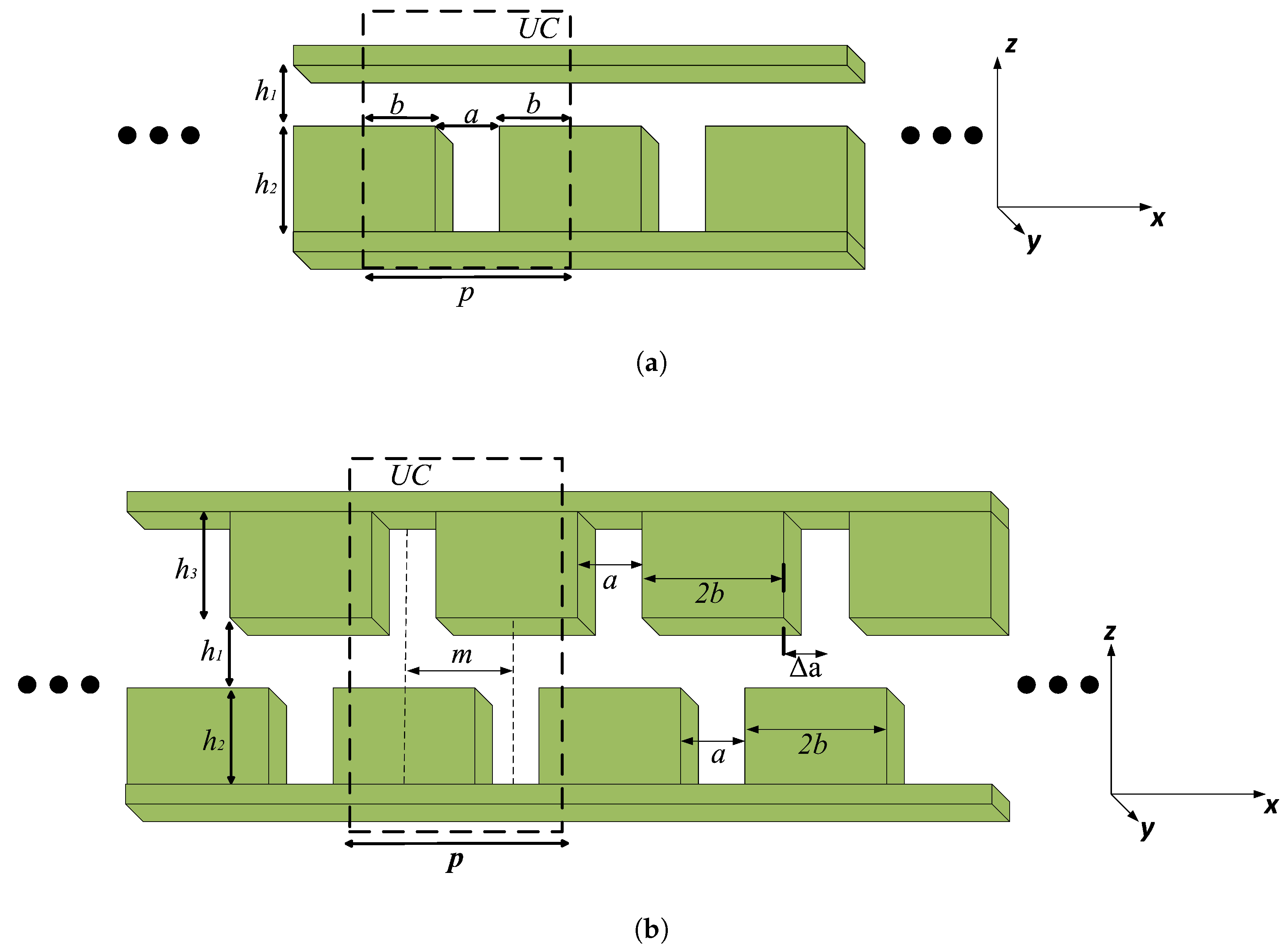
  • Step 1: Select single/glide-symmetric double CPPW model and start appropriate unit cell configuration.
  • Step 2: Constrain the design space so that the dimensional parameters of the unit cell based on the circuit model given in Figure 2 are in the appropriate range.
  • Step 3: Modify the dimensions in the limited design space obtained in Step 2, and determine the appropriate unit cell parameters satisfying the given design requirements employing Equation (5).
  • Step 4: Connect the designed unit cells back-to-back a finite number of times to meet the design requirements and obtain the filter responses with full-wave simulators.

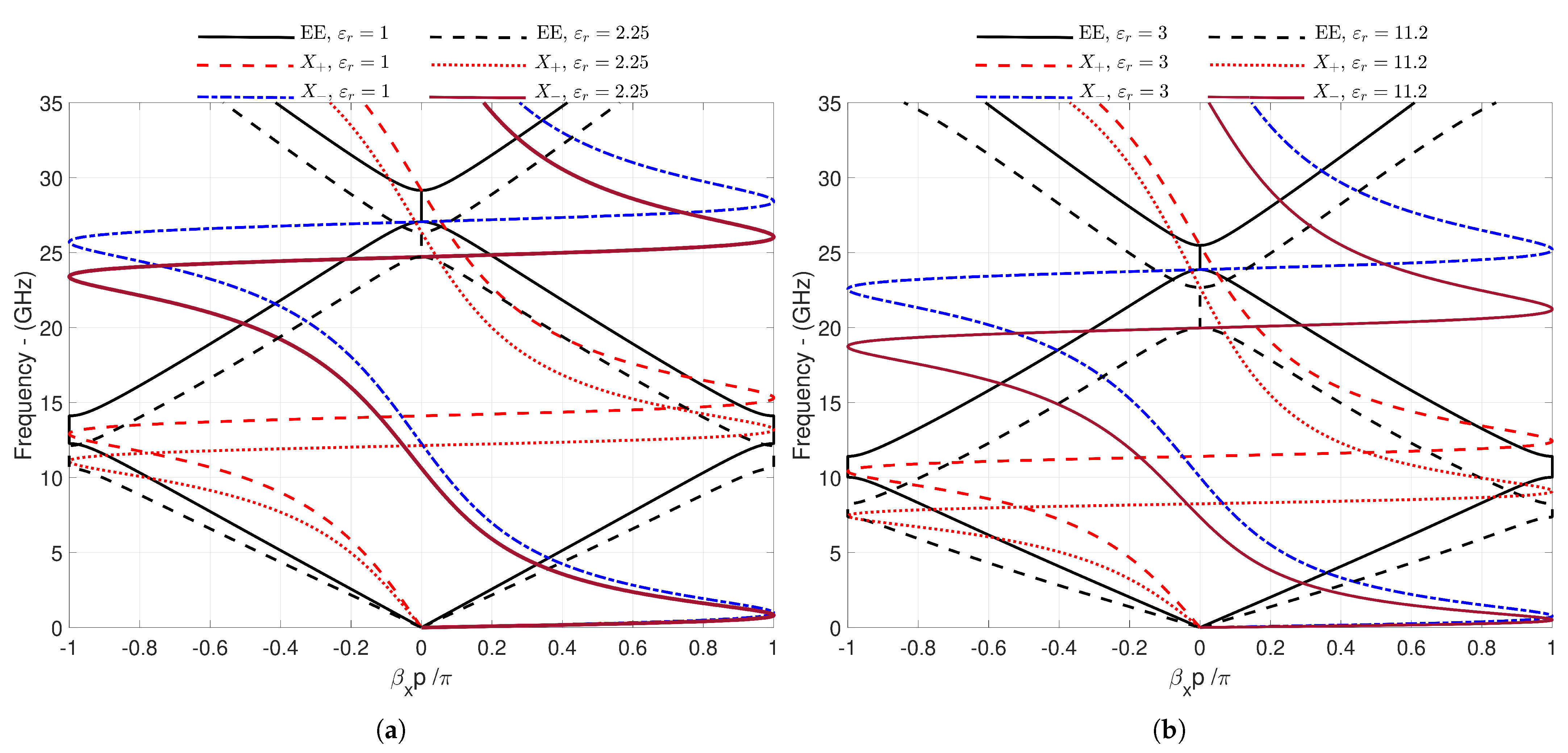
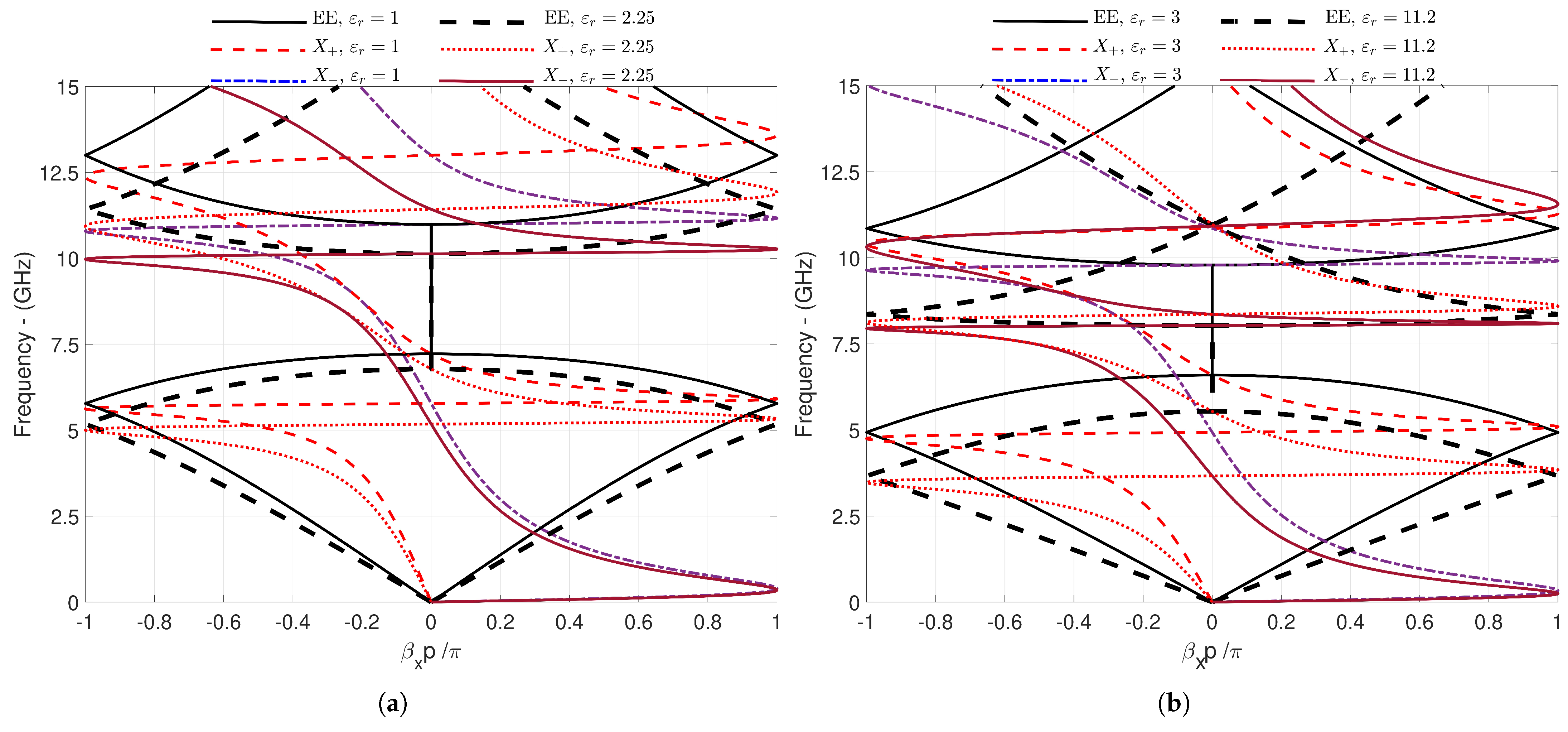
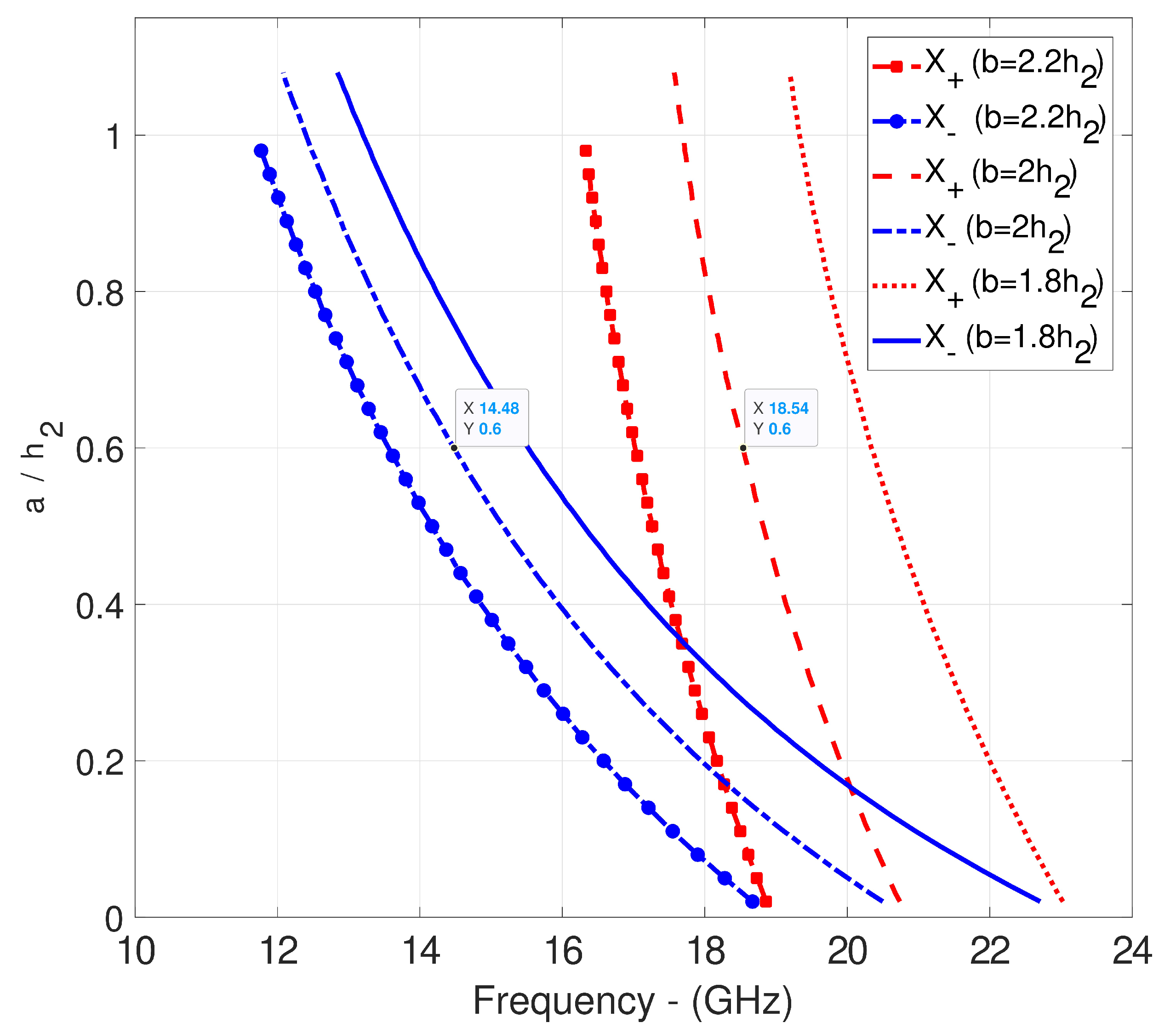
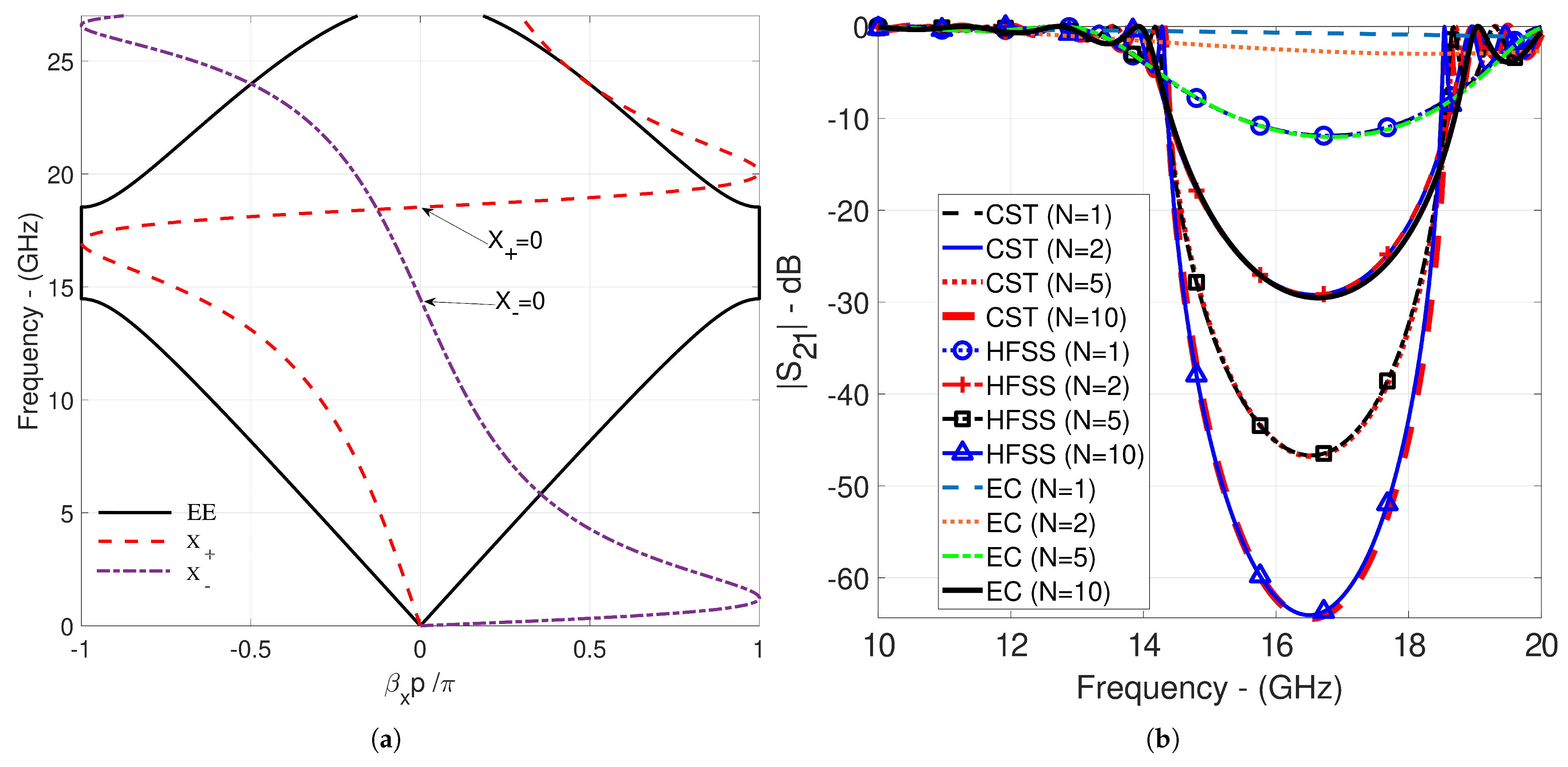
3. Results and Discussion

3.1. Numerical Examples

We first investigate the applicability of the AFGSM method for determining the passband and stopband regions of corrugated PPW structures. The final phase is dimensional synthesis in accordance with the design objectives. Figure 3 and Figure 4 serve as analysis examples to evaluate the efficacy of the AFGSM method in distinguishing passband and stopband regions including not only wide but also narrow stopbands inside single and glide-symmetric double-corrugated PPW structures. Parametric details of Figure 3a,b are given with ε r = 1 , p = 6 mm, h 1 = 3.5 mm, h 2 = 4.33 mm, a = 5.1 mm, and b = 0.45 mm and ε r = 1 , p = 9 mm, h 1 = 6 mm, h 2 = 1 mm, a = 1 mm, and b = 4 mm, respectively. All parameter values of Figure 4a,b are taken as ε r = 1 , p = 6 mm, h 1 = 3.5 mm, h 2 = h 3 = 15 mm, a = 3 mm, and b = 1.5 mm and ε r = 1 , p = 9 mm, h 1 = 10 mm, h 2 = h 3 = 1 mm, a = 0.5 mm, and b = 4.25 mm, respectively. The first and second stopbands of the periodic structure are obtained by applying the eigenvalue equation to the wide stopband example in Figure 3. These stopbands are located within the ranges of 12.14–19.58 GHz and 29.89–37.26 GHz, respectively. The AFGSM method yields the band edge frequencies of 12.136 GHz, 19.584 GHz, 29.881 GHz, and 37.263 GHz, respectively. The AFGSM method identified the band edges with a maximum difference of 6 MHz, which coincides with the results derived from the eigenvalue equation. Figure 3b presents a narrowband example, indicating the first and second stopband edges at nearly 16.33 GHz, 16.71 GHz, 32.29 GHz, and 33.43 GHz for AFGSM and EE. We achieved band edges near the eigenvalue equation in the narrow stopband scenario, with a maximum deviation of 7 MHz.
Figure 4a,b demonstrates that the zero crossings of the X + and X functions in the AFGSM method consistently align closely with the band edge frequencies in the dispersion diagrams derived from the eigenvalue equation solutions. Floquet mode transitions are observed in certain regions of the dispersion diagrams without stopbands in Figure 4a,b, with transitions occurring at 4.52 GHz and 13.49 GHz, respectively, and 16.57 GHz in Figure 4b. In these regions, the zero crossings of the X + and X functions occur at identical frequencies. Table 1 presents the band edge frequency results associated with Figure 4a,b. Based on all these analysis results, it is possible to say that Equation (5) provides an alternative method to determine the passband/stopband regions of one-dimensional corrugated PPW structures. Furthermore, the AFGSM functions clearly demonstrate the separation of the band edges, even if the stop bandwidth is narrow. The interval division root-finding routine determines the roots of the X + and X functions, eliminating the need for fine frequency sweeps and reducing the computation time by a factor of six compared to the eigenvalue equation. Figure 5 and Figure 6 illustrate the dispersion diagrams and the characteristics of auxiliary functions for single and glide-symmetric double-corrugated PPW unit cells with varying dielectric constants. Parameter values of Figure 5a,b are given as ε r = 1, ε r = 2.25, and ε r = 3, ε r = 11.2 with p = 12 mm, h 1 = 3 mm, h 2 = 0.5 mm, a = 5 mm, and b = 3.5 mm for all cases, respectively. Details of the parameters in Figure 6a,b are taken as ε r = 1, ε r = 2.25, and ε r = 3, ε r = 11.2 with p = 16 mm, h 1 = 4 mm, h 2 = h 3 = 8 mm, a = 4 mm, and b = 6 mm for all cases, respectively. The variations in the dielectric constant have evidently induced adjustments in the passband and stopband regions of the structure, and the auxiliary functions effectively demonstrate the band separation via zero crossings. We have modeled the single-corrugated and glide-symmetric double-corrugated PPW unit cell for multimode excitation (ten waveguide modes for each geometry) using the CST frequency domain solver. In the CST frequency domain solver, the S-parameters associated with the dominant mode of multimode excitation have been extracted and included in the eigenvalue equation shown in Equation (2). Furthermore, all S-parameters derived from CST have been included in Equation (4). Figure 7 and Figure 8a illustrate the dispersion diagrams for all operations and the characteristics of the auxiliary functions. These results indicate that the simulator-assisted AFGSM functions are indistinguishably identical to the eigenvalue equations derived from CST and the equivalent circuit (EC) at the band edges. In Figure 8a, the band edge frequency derived from the eigenvalue equation of EC at about 12 GHz seems higher. This variation is due to a limited level of high-order mode interaction inside the circuit model. Parametric details of Figure 7 and Figure 8 are given as ε r = 1, p = 8.28 mm, h 1 = 1 mm, h 2 = 1.8 mm, a = 1.08 mm, and b = 3.6 mm and ε r = 1, p = 26.5 mm, h 1 = 0.5 mm, h 2 = h 3 = 2 mm, a = 1.5 mm, and b = 12.5 mm, respectively. Figure 7b demonstrates that the stopband of the structure extends exclusively owing to the gradual increase in h 2 . We investigated manufacturing tolerances in Figure 8b by slowly changing the glide symmetry of the structure. The offset or gradual breaking of the glide symmetry of one corrugation results in the broadening of the structure’s stopband.
In order to apply the dimensional design approach, the following two design objectives were identified:
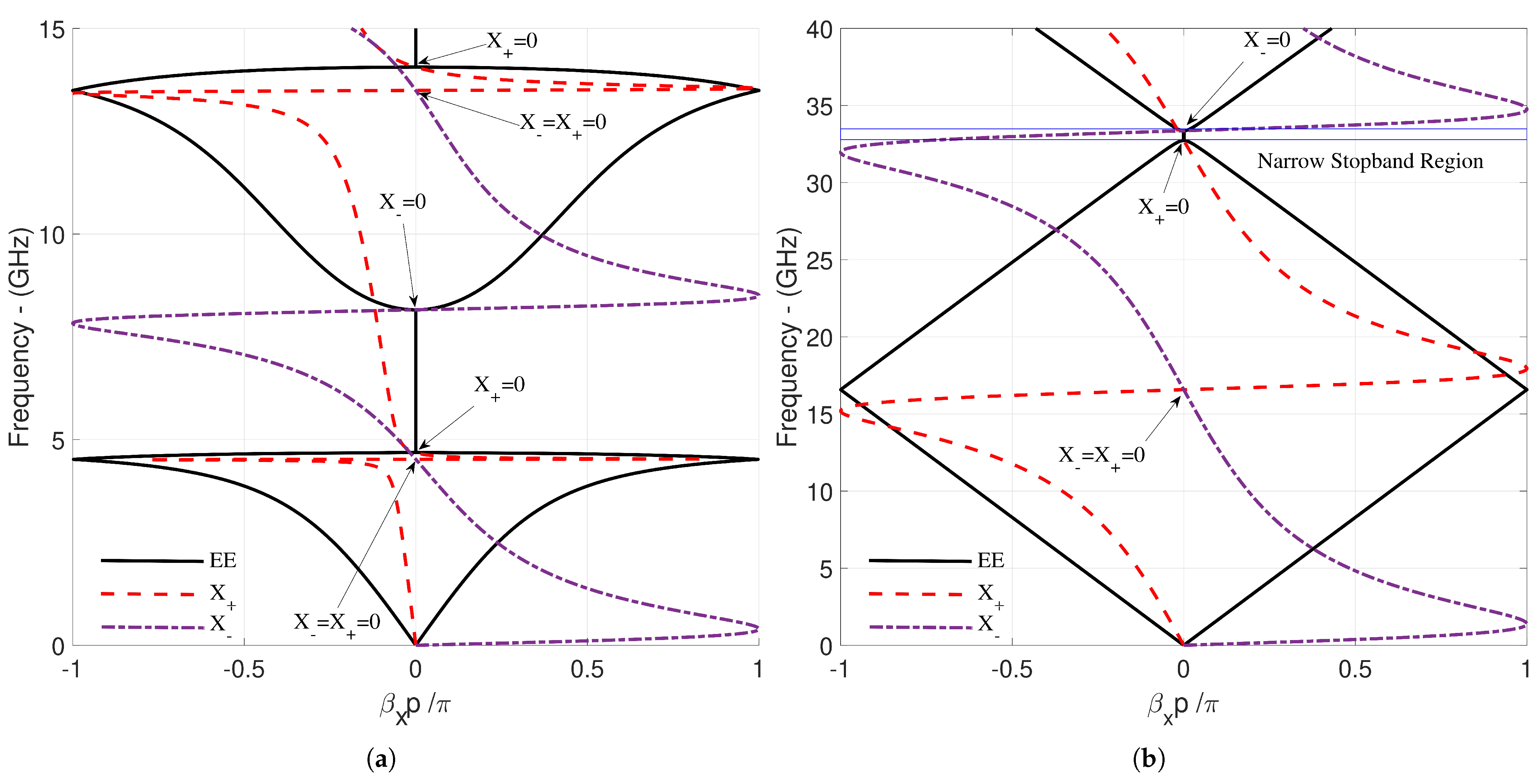
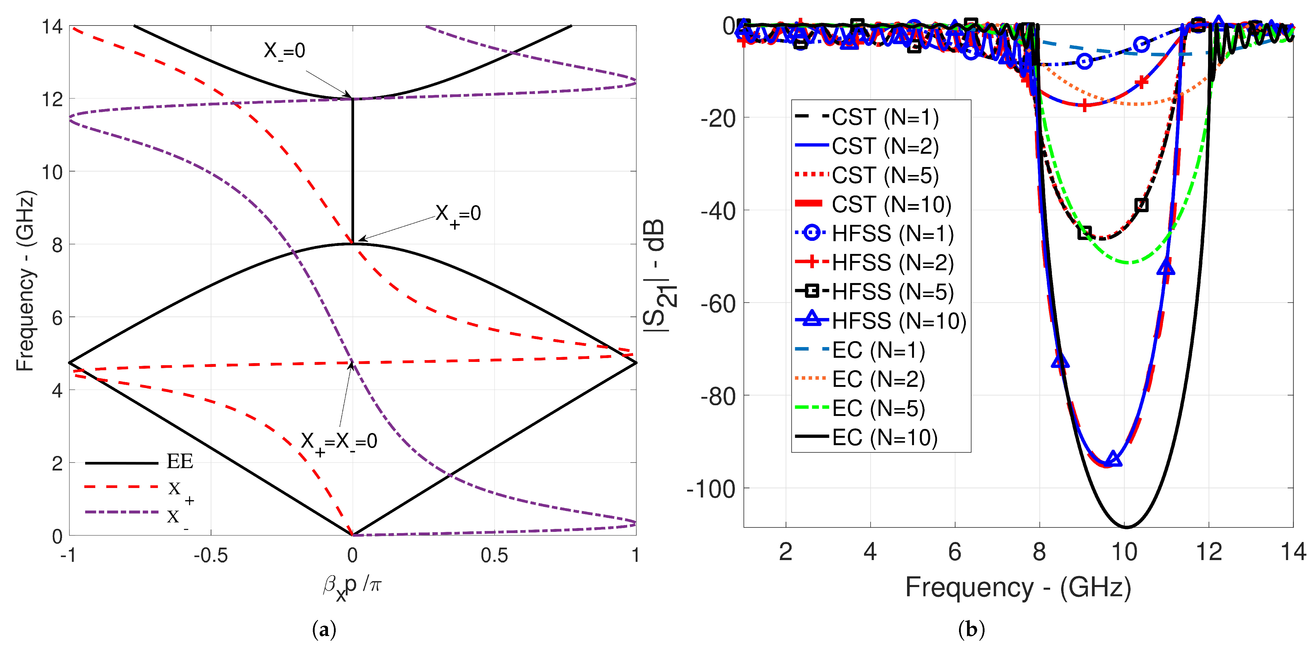
  • (a) Ku-band filter design with a suppression level of more than −50 dB in the 15.20–17.78 GHz range for a single CPPW.
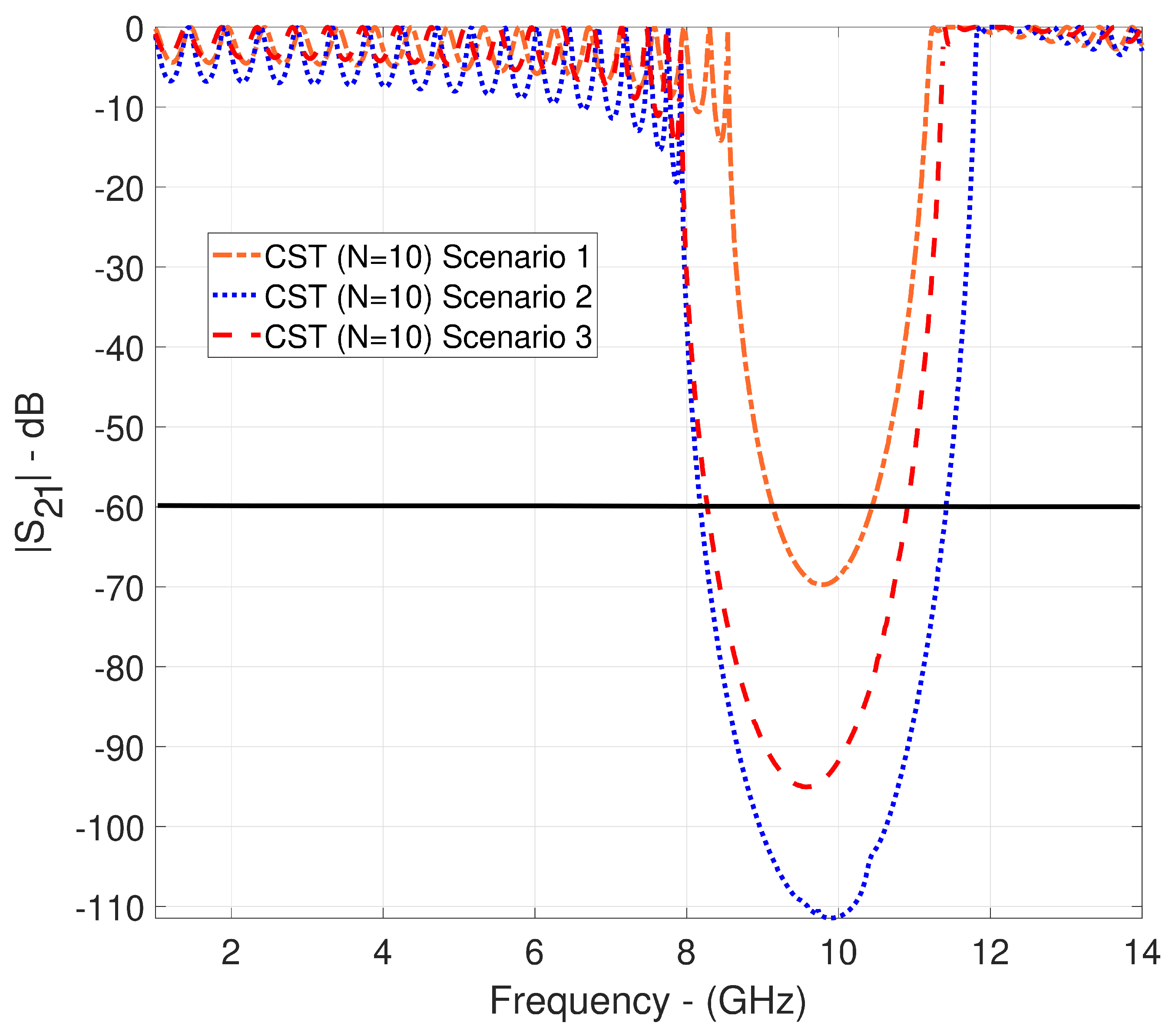
  • (b) X-band filter design with a suppression level of more than −60 dB in the 8.27–10.91 GHz range for glide-symmetric double CPPWs.

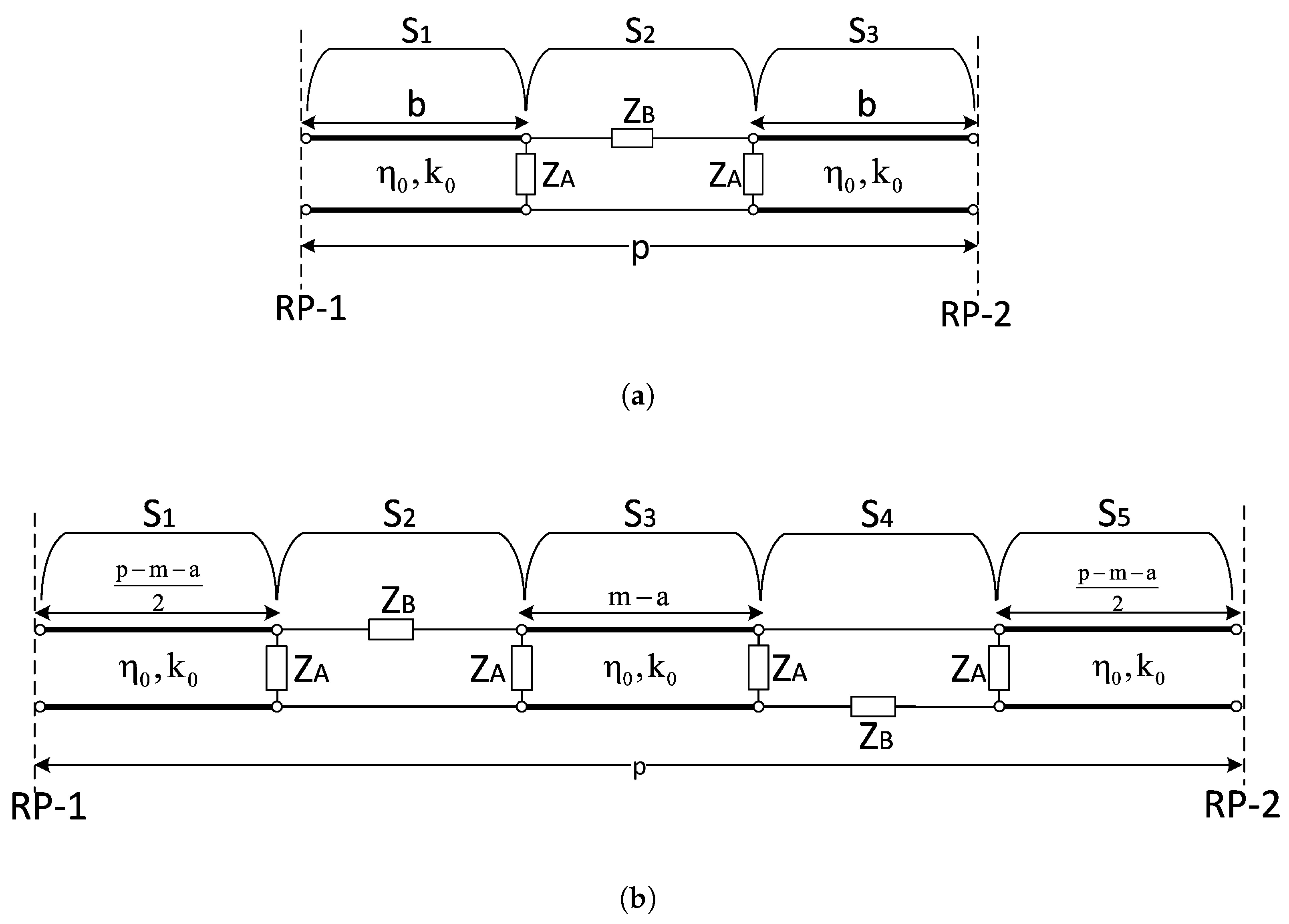
3.2. Design of Unit Cell and Cascade Connection Analysis of Corrugated PPW Structures

The design phase begins with the selection of an appropriate unit cell model. We select the initial parameters h 1 = 1 mm, h 2 = 1.8 mm, a = 0.8 h 2 , and b = 2.2 h 2 for the air-filled single-corrugated PPW model. This selection implements the design procedure as outlined in the initial step. At this point, the design of the unit cell transitions to the determination of the critical parameters of the design geometry. Figure 9 illustrates the relationship between the geometrical parameters of the AFGSM functions and the zero crossings across various frequencies. In the second step, the design procedure maintains the constrained design spaces (with respect to h 1 and h 2 for h 1 = 1 mm and h 2 = 1.8 mm) while restricting a and b to specific ranges, as illustrated in Figure 9. The variations given in this figure provide a solution for obtaining the parameters corresponding to the targeted stopband bandwidth for the parameters under investigation.
Step 3 investigates the variation in X + and X functions for the dimensions in the limited design space obtained in step 2. Figure 9 illustrates that the X + and X functions for the lines b = 2 h 2 and a = 0.6 h 2 possess a stopband that satisfies the design requirements, as depicted for X and Y point pairs. The AFGSM method enables the initial selection and simultaneous modelling of specific geometric parameters within the frequency range that meets design criteria, offering the designer precise alternatives for determining the optimal geometry of the unit cell, as demonstrated in Figure 9. In the final step, Figure 10a shows the dispersion diagram of the designed unit cell, satisfying the suppression-level design criterion. We obtained a unit cell design with a stopband of 4.06 GHz bandwidth and a center frequency of 16.51 GHz. To test the band properties, we connected unit cells back to back in varying numbers, as illustrated in Figure 10b. Figure 10b shows that the full-wave electromagnetic solver results are quite compatible. The | S 21 | -dB results of the EC model for the cascade-connected single-corrugated PPW unit cells exhibit a less deep stopband region in contrast to the | S 21 | -dB results from the full-wave electromagnetic model of the structure. The EC model is inadequate for accurately representing the discontinuities in the cross-sections for this structure. Discontinuities in the sections result in the excitation of high-order modes. Only the reactive components on the junction planes receive evaluation for high-order mode interactions in the circuit model [36]. Mode-matching methods may be used on these structures to obtain results comparable to full-wave electromagnetic simulation outcomes [31]. As it is well-known in periodic structures, increasing the number of unit cells leads to a deeper stopband in single CPPWs. In this example, we ensured adequate design requirements by increasing the number of unit cells (N) to 10.
For glide-symmetric double CPPW structures, we set the parameters to a = 1 mm, h 1 = 0.5 mm, h 2 = h 3 = 1 mm, and b = 12.4 mm. This selection implements the design procedure as outlined in the initial step. We limited the a and h 2 = h 3 parameters to 1–2.5 mm and b to 12.4–13.6 mm at intervals of 0.1 mm by creating multiple design spaces and preserving the glide-symmetry case. This limitation significantly reduces the computational burden in achieving the design requirements. In the design space, the stopband edges of the first stopband region for each parameter are found and recorded using X + and X functions. We obtained a significant dataset on a large scale, determining the band edge frequencies determined by the AFGSM functions in the constrained design space. The dataset contains a variety of selectable stopband frequencies and the stopband widths situated at these centers. We have selected a center frequency in this context that can cover the targeted stopband. From this set of data, Equation (5) pulls out the values for different dimensions with a center frequency of 10 GHz, different stop bandwidth values, and a certain frequency deviation ( δ ), as shown in Table 2. The AFGSM method offers various design dimensions for identifying appropriate unit cell parameters via multi-geometric parameter optimization, as illustrated in Table 2. The crucial aspect prior to dimensional design, as illustrated in the dataset of the second example, is to restrict the design area to a defined region. In this case, the AFGSM approach guarantees the quick and precise operation of the design algorithm. At this point, three scenarios, bold and italicized in Table 2, have been selected to meet the design requirements of the dimensional design applicability of Equation (5) for the same and different stop bandwidths.
Figure 11, Figure 12 and Figure 13 illustrate dispersion diagrams and the dominant mode of the | S 21 | frequency characteristics derived from various finite periodic configurations of designed unit cells throughout three selected scenarios. All AFGSM function behaviors and dispersion characteristics of all scenarios given in Figure 11a, Figure 12a, and Figure 13a indicate that the roots of the AFGSM functions can efficiently seperate passband/stopband regions. The analysis of the filtering characteristics obtained by cascading the unit cells was performed in CST Microwave Studio and HFSS simulation environments. In order to model one-dimensional corrugated PPWs in CST and HFSS, it was necessary to assign appropriate boundary conditions. For this purpose, in CST, electric ( E t = 0) and magnetic ( H t = 0) conditions were used; in HFSS, perfect E and perfect H boundary conditions were assigned to the top, bottom, and side walls of the considered structures, respectively. The same computer was used to run the simulations of CST, HFSS, and our code of the proposed method. The ordinary laptop had an Intel (R) Core (TM) i7-6700HQ CPU@2.6 GHz with 16 GB RAM. In the examined structures, the first ten dominant waveguide modes of excitation were satisfied to perform with the waveguide port in CST and with the waveport in HFSS, and the frequency characteristics of the first dominant mode of | S 21 | were investigated. Obtaining the dataset in the given limited design space took 360 h with CST Eigen Mode Solver, while solving the eigenvalue equation based on the circuit model took 612 s. The same dataset was generated in 20 s using the AFGSM method. We observe from Figure 11a that Scenario 1’s band edges were 8.648 GHz and 11.344 GHz. In the first scenario, we selected a stop bandwidth of 2.7 GHz and determined the dimensions using the AFGSM functions, with a deviation of 10 MHz. The filtering characteristics of the unit cell designed in Scenario 1 with different numbers of finite periodic arrays are given in Figure 11b. The periodic arrangement of the geometry considered in Scenario 1 significantly increased the passband fluctuation levels, as shown in Figure 11b. However, it is evident that the design specifications have not yet reached their target. Selecting unit cell parameters with a broader stopband would prove beneficial in terms of both size and design goals. Figure 12b unequivocally illustrates that a periodic arrangement with N = 10 adequately fulfills the design specifications, and the passband ripple levels are considerable. The specified design requirements primarily provide the starting stopband frequency for the suppression level but do not determine the required stop bandwidth in Figure 13b.
Figure 11 and Figure 12b illustrate that the results of the full-wave electromagnetic simulation and the EC model converge with an increasing number of unit cells. In Figure 13b, although an EC simulation result that aligned with the required stopband was achieved, it was noted that the full-wave electromagnetic simulation results yielded a smaller and less deep stopband region. The discrepancies occur due to the placement of the anticipated stopband region in the upper modes of the dispersion diagram, the prominence of discontinuity regions inside the structure, and the resultant increase in higher-order mode interactions. The single-corrugated and glide-symmetric double-corrugated PPW designed bandstop filters for two examples exhibit ripples outside the band. Figure 10b–Figure 13b indicate that these ripples are at lower levels in the substantially single-corrugated PPW filter. In the X-band filter designs, significant ripples have been observed, particularly in the low passbands. The characteristics of the periodic arrangement anticipate these ripples. Furthermore, Figure 11, Figure 12 and Figure 13 clearly demonstrate that the use of glide symmetry enhances the ripples generated by the periodic design. In this situation, passband ripples can be managed using a different design method that employs the AFGSM algorithm, either by adjusting the unit cell parameters of the broken glide symmetry [15,27,37,42,51,52,53] or by examining each unit cell parameter with tapering technology [15,54]. These solutions are not investigated here due to the stopband characteristics of the periodic arrangements of the GS-DCPPW unit cell only being taken into account for testing purposes. The frequency characteristics of | S 21 | , with a constant unit cell count of N = 10 for all selected scenarios, are presented in Figure 14.
Table 3 presents the design unit cell parameter values for all scenarios and the overall filter dimensions achieved for N = 10. Currently, there are trade-offs regarding filter performance and dimensions for the scenarios given in Figure 14 and Table 3. Initially, fulfilling the design specifications of Scenario 1 will evidently necessitate an increased number of unit cells. This circumstance will lead to a substantial increase in passband ripple levels. Consequently, Scenario 1 fails to satisfy the design specifications. Scenario 2 satisfies the design specifications with an identical quantity of unit cells, in contrast to the other two scenarios, which utilize varying sizes yet yield the same stopband width. Furthermore, the overall filter length of Scenario 2 is shorter than that of Scenario 3, presenting a compact design possibility. Conversely, while Scenario 3 does not entirely fulfill the design specifications, its ripple levels in the passband surpass those of Scenario 2, thereby providing a design advantage to Scenario 3. Table 3 shows that Scenario 3 provides a compact design that is advantageous in terms of filter height. In glide-symmetrical double CPPWs, the frequency characteristics of | S 21 | , illustrated by the finite periodic combinations in Figure 11b, Figure 12b, and Figure 13b, indicate that frequency behaviors of the cascaded unit cell begin to approach the center frequency of the stopband depicted in Table 2 as the number of unit cells increases. The situation is important to consider in ascertaining the designer’s requirements. Utilizing this knowledge, the designer begins the design by selecting a higher stopband center frequency, extracting the unit cell design parameters from the AFGSM functions and trying to ascertain the design requirements. The AFGSM method finds different solutions that meet the same design criteria. These solutions allow you to choose the unit cell with the smallest dimension possible, which makes it easier to create small designs.
Table 4 compares the performance of designed periodic bandstop filters with similar performances reported in the open literature. The designed filter exhibits a broader suppression level bandwidth (SLBW) and achieves more compact design according to [5]. Bandstop filter designs based on microstrip technology given in [55,56,57] have notably compact configurations. Ref. [55] has a similar suppression level as Scenario 2, whereas the designed filter demonstrates a wider stopband bandwidth. However, Refs. [56,57] show higher suppression characteristics and narrow bandwidths with respect to the developed filter. One clearly states that despite the conventional cavity BPF design given in [58] having small dimensions, the suppression level bandwidth could not be as wide as the designed filter. It can be revealed that although the BPF design based on hybrid (microstrip–stripline) technology [58] depicts compact dimensions, the developed filter has a wider suppression level. A major drawback of the developed filter is its very high fluctuation levels in the passband. Conversely, we note that the stopband slope is superior to other designs except [5,58] for the upper transition band, respectively. However, regarding the normalized circuit size, the performance of the proposed filter is slightly lower compared to other designs.
The AFGSM approach relies on the S-parameters of the unit cell, which emphasize the need to ascertain the S-parameters of the structure. One of the easiest ways to carry these calculations out is by utilizing the equivalent circuit model of the investigated periodic structure. Ref. [36] provides that the impact of glide symmetry is obviously identical to merely reducing the spatial period by half. This equivalent circuit model addresses the impact of the glide symmetry of the periodic structure within the AFGSM approach. The demonstrated equivalent circuit model, if it supports multimode excitation, enables the extraction of precise information on the passband/stopband regions of the studied geometry via Equation (4). If the model supports single-mode excitation, we can derive comprehensive information using Equation (5). Adapting the multimode equivalent circuit model [19] to glide-symmetric periodic structures like GS-DCPPWs and, in this direction, modeling 1D and 2D periodic structures such as frequency-selective surfaces [19], holey metasurfaces [29], tapered/non-tapered corrugated planar transmission lines [31,59,60], and composite FHMSIW/SSPP waveguides [61,62,63] for determining band edges using reformulated or novel AFGSM functions and comparing the results with full-wave simulators could be an important future study. Furthermore, using full-wave electromagnetic simulators provides the ability to gather scattering characteristics for all structures analyzed under multimode excitation via frequency domain analysis of the unit cell. Incorporating the scattering parameters derived from this point of origin into Equation (4) establishes the full-wave simulation-assisted AFGSM method. The investigation or design of the complex periodic structures described in [59,60,61,62,63] may be performed using the AFGSM methodology. In this context, the inclusion of higher-order modes enhances the precision of the resulting analysis or design results. This condition results in an increase in computation time. The mode-matching methodology yields the S-parameters of the unit cell, and when included in the AFGSM method, it may decrease computing time.

4. Conclusions

This study aimed to investigate the potential of the AFGSM method in analyzing and designing corrugated parallel-plate waveguide unit cells. The AFGSM method made it simple to find the passband and stopband regions of single and glide-symmetric double CPPW periodic structures. This method led to the development of a novel design procedure for filter designs with CPPW structures. We demonstrate that we can design glide-symmetric double CPPW filters using the AFGSM method. The design procedure demonstrates the ability to determine the minimum unit cell size. The proposed method and design procedure yield a bandstop filter characteristic that is more compact and has a high degree of suppression bandwidth. The AFGSM method allows for thorough studies of the bandgap in corrugated parallel-plate waveguides, no matter the mode number, and it also helps in checking initial manufacturing tolerances.

Author Contributions

Conceptualization, F.Ç. and A.O.E.; methodology, F.Ç. and A.O.E.; software, F.Ç. and A.O.E.; validation, F.Ç. and A.O.E.; analysis, F.Ç. and A.O.E.; investigation, F.Ç. and A.O.E.; resources, F.Ç. and A.O.E.; writing—original draft preparation, F.Ç.; writing—review and editing, A.O.E.; visualization, F.Ç. and A.O.E.; supervision, A.O.E.; project administration, A.O.E. All authors have read and agreed to the published version of the manuscript.

Funding

This research received no external funding.

Institutional Review Board Statement

Not applicable.

Informed Consent Statement

Not applicable.

Data Availability Statement

The data that support the findings of this study are available from the corresponding author upon request.

Conflicts of Interest

The authors declare no conflicts of interest.

Abbreviations

The following abbreviations are used in this manuscript:
MM-GSMMode Matching–Generalized Scattering Matrix
BSFBand Stop Filter
HFSSHigh-Frequency Structure Simulator
CSTComputer Simulation Technology
FHMSIWFolded Half-Mode Substrate Integrated Waveguide
SSPPSpoof Surface Plasmon Polaritons
UCUnit Cell

Appendix A. Network Representation Explanation of Expanded Version of Equivalent Circuit of Corrugations and Obtaining S-Parameters of Unit Cell with All Definitions

To find the scattering matrices of all structures belonging to the unit cells given in Figure 2, it is necessary to find the scattering matrix of each block element S i ( i = 1 , 2 , . . . , 5 ) . Since blocks S1, S3, and S5 in Figure 2 are conventional transmission lines, the scattering parameters of a lossless transmission line of length l are defined as follows:
[ S T L ] = 0 e j k 0 l e j k 0 l 0 .
By replacing l and k 0 = 2 π f / c (where f and c are the frequency and speed of light) with the length and phase constant of the block under consideration, the scattering parameters for blocks S1, S3, and S5 can be found. In this case, l is b for S1 and S3 in a single-corrugated PPW; in a glide-symmetric double-corrugated PPW, it is (pma)/2 for S1 and S5 and (ma) for S3. S2 and S4 circuits play a crucial role in determining the scattering parameters of the unit cells in the corrugated PPW structures under study. To clarify this situation, the open forms of the π circuits (S2 and S4) are given in Figure A1a,b, with series stubs reduced in Figure 2.
Figure A1. Full view of π circuit in (a) S2 and (b) S4 blocks given in Figure 2.
Applsci 15 05876 g0a1
The reactive elements indicated in Figure A1a,b are located at the junctions to account for higher-order mode interactions [36]. The corrugations consist of a series of stubs terminated with a short circuit. Impedance expressions ( Z A and Z B ) for the reduced forms of the π circuits mentioned in this work are given. Figure A1 presents the derivation of Z A and Z B in a sequentially numbered format. In step 1, Y A is first derived using the provided equality Y A = j B a , followed by the calculation of Z A as Z A = 1 / Y A [49].
B a = 2 a λ 0 η 0 [ tan 1 ( 1 / α ) + ln ( 1 + α 2 ) α ]
The equality in Equation (A2) is represented by α , λ 0 , and η 0 , corresponding to a / 2 h 1 , 2 π / k 0 , and 120 π , respectively. In step 2, the impedance of the transmission line Z s h i ( i = 2 , 3 ) = j η 0 tan ( k 0 h i ) ( i = 2 , 3 ) , which is terminated by a short circuit, is considered. The admittance of this structure Y s h i ( i = 2 , 3 ) = 1 / Z s h i is derived from this point. Here, η 0 is equal to η 0 a h 1 [49,64]. In step 3, the admittance Y d = j B d of the capacitor linked to Y s h i is determined using the equations shown below [49]:
B d = h 1 λ 0 η 0 ( π 3 α + A 2 )
A 2 = 2 [ α tan 1 ( 1 / α ) + tan 1 ( α ) α + ln ( 1 + α 2 4 α ) π ( 1 + α 2 ) 6 α ] A 1
A 1 = 2 α π e ( 2 tan 1 ( α ) α ) [ 1 + 5 + α 2 4 ( 1 + α 2 ) e ( 2 tan 1 ( α ) α ) + [ 4 1 + α 2 + ( 5 α 2 1 + α 2 ) 2 ] e ( 4 tan 1 ( α ) α ) 9 ]
In step 4, Z e may be computed using Y d and Y s h i derived in steps 2 and 3, as Z e = 1 / ( Y s h i + Y d ) . The admittance of the inductance specified in step 5, Y c = j B c , is calculated using the given equation, and Z c = 1 / Y c is found [49].
B c = λ 0 ( 2 π a η 0 )
In step 6, the admittance Y f = 1 / ( Z e + Z c ) is found using the impedances Z c and Z e obtained in steps 4 and 5. In step 7, the admittance of the inductance specified is found using the following equation [49]:
B b = [ B a [ ( 2 h 1 λ 0 η 0 ) ( π α 3 + A 1 ) ] ] 2
In step 8, using the admittances Y f and Y 1 found in steps 6 and 7, Z B = 1 / ( Y f + Y 1 ) is obtained. Thus, all the Z A and Z B impedances given in Figure 2 can be easily determined. The π circuits given in Figure A1a,b are symmetrical circuits, and the scattering parameters are defined below:
S 11 π = S 22 π = { [ ( η 0 | | Z A ) + Z B ] | | Z A } η 0 { [ ( η 0 | | Z A ) + Z B ] | | Z A } + η 0
S 21 π = S 12 π = ( 1 + S 11 ) η 0 | | Z A ( η 0 | | Z A ) + Z B
After the scattering matrices of each S i ( i = 1 , 2 , . . . , 5 ) block circuit are found, the scattering matrices of the blocks are cascaded as [ S A ] and [ S B ], respectively, by the following equations, and the scattering parameters of the unit cell are obtained:
S 11 = S 11 A + S 12 A S 11 B S 21 A 1 S 22 A S 11 B
S 12 = S 12 A S 12 B 1 S 11 B S 22 A
S 21 = S 21 B S 21 A 1 S 22 A S 11 B
S 22 = S 22 B + S 21 B S 22 A S 12 B 1 S 11 B S 22 A

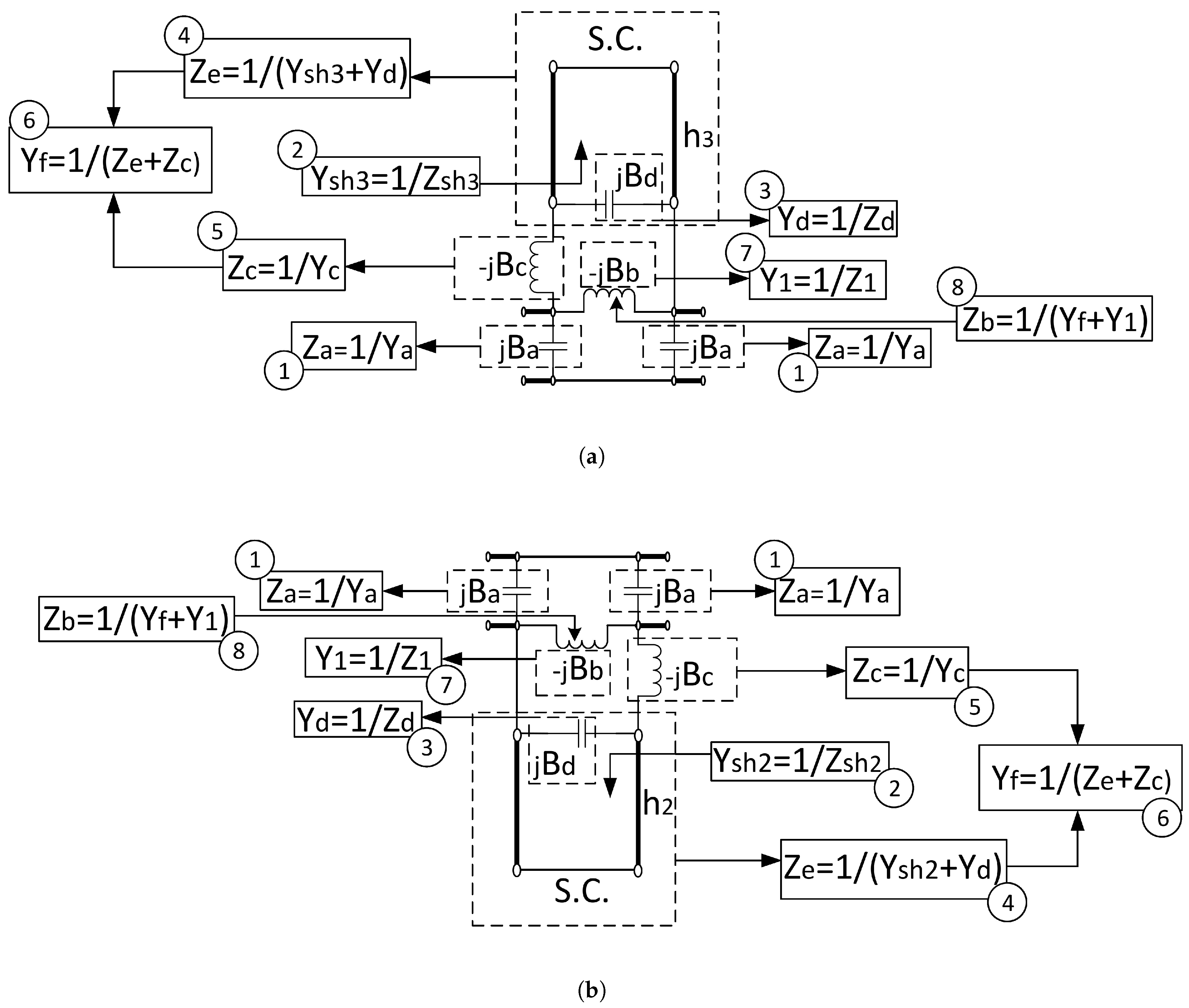
Appendix B. Notation List

A ( f ) , D ( f ) The A and D elements of ABCD parameters
aThe corrugate width of single and glide-symmetric double CPPW
a 1 , b 1 The normalized power waves used in scattering parameters
bThe length of half of each ridge in the CPPW
β x The Floquet phase factor propagating in the x direction
δ The frequency deviation
Δ f The width of the stopband
ε r The dielectric constant of the material loaded in the CPPW
E t The tangential component of the electric field
fThe frequency
f 1 The last frequency of the stopband
f 2 The first frequency of the stopband
h 1 The height between corrugated parallel plates
h 2 The height of the bottom section of corrugated parallel plates
h 3 The height of the top section of corrugated parallel plates
H t The tangential component of the magnetic field
I The block identity matrix
lThe length of any transmission line
λ The eigenvalue
mThe gliding operator
NThe number of unit cells
pThe period of the periodic structure
S 11 , S 12 , S 21 , S 22 The elements of a classical scattering matrix of a two-port network
S 11 , S 12 , S 21 , S 22 The block submatrices of the generalized scattering matrix
X ± f u l l The complete form of auxiliary functions
X ± The reduced form of auxiliary functions

References

  1. Hessel, A.; Chen, M.H.; Li, R.C.; Oliner, A.A. Propagation in periodically loaded waveguides with higher symmetries. Proc. IEEE 1973, 61, 183–195. [Google Scholar] [CrossRef]
  2. Navarro, M.S.; Rozzi, T.E.; Lo, Y.T. Propagation in a rectangular waveguide periodically loaded with resonant irises. IEEE Trans. Microw. Theory Tech. 1980, 8, 857–865. [Google Scholar] [CrossRef]
  3. Amari, S.; Vahldieck, R.; Bornemann, J.; Leuchtmann, P. Spectrum of corrugated and periodically loaded waveguides from classical matrix eigenvalues. IEEE Trans. Microw. Theory Tech. 2000, 3, 453–460. [Google Scholar] [CrossRef]
  4. Lech, R.; Mazur, J. Propagation in rectangular waveguides periodically loaded with cylindrical posts. IEEE Microw. Wirel. Compon. Lett. 2004, 14, 177–179. [Google Scholar] [CrossRef]
  5. Simsek, S.; Topuz, E. Some properties of generalized scattering matrix representations for metallic waveguides with periodic dielectric loading. IEEE Trans. Microw. Theory Tech. 2007, 11, 2336–2344. [Google Scholar] [CrossRef]
  6. Othman, M.A.K.; Pan, X.; Atmatzakis, G.; Christodoulou, C.G.; Capolino, F. Experimental demonstration of degenerate band edge in metallic periodically loaded circular waveguide. IEEE Trans. Microw. Theory Tech. 2017, 11, 4037–4045. [Google Scholar] [CrossRef]
  7. Ertay, A.O.; Simsek, S. Detection of band edge frequencies in symmetric/asymmetric dielectric loaded helix slow-wave structures. Int. J. Circuit Theory Appl. 2022, 50, 507–524. [Google Scholar] [CrossRef]
  8. Petek, M.; Rico-Fernández, J.; Vásquez, J.A.T.; Valerio, G.; Mesa, F.; Quevedo-Teruel, O.; Vipiana, F. Numerical Modelling of Higher-Symmetric Periodic Structures with Hexagonal Lattice. IEEE Trans. Antennas Propag. 2025, 73, 1650–1661. [Google Scholar] [CrossRef]
  9. Tahir, G.; Hassan, A.; Ali, S.; Bermak, A. Unit Cell Optimization of Groove Gap Waveguide for High Bandwidth Microwave Applications. Appl. Sci. 2024, 14, 10891. [Google Scholar] [CrossRef]
  10. Jimenez-Suarez, J.M.; Mesa, F.; Quevedo-Teruel, O. A Symmetry-Based Multimodal Transfer-Matrix Method for the Analysis of 2D-Periodic Structures. IEEE Trans. Microw. Theory Tech. 2025, 1–11. [Google Scholar] [CrossRef]
  11. Şimşek, S.; Topuz, E.; Niver, E. A novel design method for electromagnetic bandgap based waveguide filters with periodic dielectric loading. AEU-Int. J. Electron. Commun. 2012, 66, 228–234. [Google Scholar] [CrossRef]
  12. Coves, A.; San-Blas, A.A.; Bronchalo, E. Analysis of the dispersion characteristics in periodic Substrate Integrated Waveguides. AEU-Int. J. Electron. Commun. 2021, 139, 153914. [Google Scholar] [CrossRef]
  13. Mesa, F.; Rodríguez-Berral, R.; Medina, F. On the computation of the dispersion diagram of symmetric one-dimensionally periodic structures. Symmetry 2018, 10, 307. [Google Scholar] [CrossRef]
  14. Ertay, A.O.; Şimşek, S. A comprehensive auxiliary functions of generalized scattering matrix (AFGSM) method to determine bandgap characteristics of periodic structures. AEU-Int. J. Electron. Commun. 2018, 94, 139–144. [Google Scholar] [CrossRef]
  15. Karamirad, M.; Pouyanfar, N.; Alibakhshikenari, M.; Ghobadi, C.; Nourinia, J.; See, C.H.; Falcone, F. Low-loss and dual-band filter inspired by glide symmetry principle over millimeter-wave spectrum for 5G cellular networks. Iscience 2023, 26, 1–14. [Google Scholar] [CrossRef]
  16. Xu, S.; Wu, J.; Chen, X. Design of Broadband Highly Efficient Power Amplifier Based on Low-Pass Filtering Network with Periodic Structure. Int. J. Circuit Theory Appl. 2024. [Google Scholar] [CrossRef]
  17. Liu, Z.; Lu, H.; Liu, J.; Yang, S.; Liu, Y.; Lv, X. Compact fully metallic millimeter-wave waveguide-fed periodic leaky-wave antenna based on corrugated parallel-plate waveguides. IEEE Antennas Wirel. Propag. Lett. 2020, 19, 806–810. [Google Scholar] [CrossRef]
  18. Maci, S.; Minatti, G.; Casaletti, M.; Bosiljevac, M. Metasurfing: Addressing waves on impenetrable metasurfaces. IEEE Antennas Wirel. Propag. Lett. 2011, 10, 1499–1502. [Google Scholar] [CrossRef]
  19. Alex-Amor, A.; Mesa, F.; Palomares-Caballero, Á.; Molero, C.; Padilla, P. Exploring the potential of the multi-modal equivalent circuit approach for stacks of 2-D aperture arrays. IEEE Trans. Antennas Propag. 2021, 69, 6453–6467. [Google Scholar] [CrossRef]
  20. Quevedo-Teruel, O.; Valerio, G.; Sipus, Z.; Rajo-Iglesias, E. Periodic structures with higher symmetries: Their applications in electromagnetic devices. IEEE Microw. Mag. 2020, 21, 36–49. [Google Scholar] [CrossRef]
  21. Palomares-Caballero, Á.; Alex-Amor, A.; Padilla, P.; Valenzuela-Valdés, J.F. Dispersion and filtering properties of rectangular waveguides loaded with holey structures. IEEE Trans. Microw. Theory Tech. 2020, 68, 5132–5144. [Google Scholar] [CrossRef]
  22. Quevedo-Teruel, O.; Chen, Q.; Mesa, F.; Fonseca, N.J.; Valerio, G. On the benefits of glide symmetries for microwave devices. IEEE J. Microwaves 2021, 1, 457–469. [Google Scholar] [CrossRef]
  23. Ghasemifard, F.; Norgren, M.; Quevedo-Teruel, O. Twist and polar glide symmetries: An additional degree of freedom to control the propagation characteristics of periodic structures. Sci. Rep. 2018, 8, 11266. [Google Scholar] [CrossRef] [PubMed]
  24. Dahlberg, O.; Mitchell-Thomas, R.; Quevedo-Teruel, O. Reducing the dispersion of periodic structures with twist and polar glide symmetries. Sci. Rep. 2017, 7, 10136. [Google Scholar] [CrossRef]
  25. Arnberg, P.; Barreira Petersson, O.; Zetterstrom, O.; Ghasemifard, F.; Quevedo-Teruel, O. High refractive index electromagnetic devices in printed technology based on glide-symmetric periodic structures. Appl. Sci. 2020, 10, 3216. [Google Scholar] [CrossRef]
  26. Ebrahimpouri, M.; Quevedo-Teruel, O.; Rajo-Iglesias, E. Design guidelines for gap waveguide technology based on glide-symmetric holey structures. IEEE Microw. Wirel. Compon. Lett. 2017, 27, 542–544. [Google Scholar] [CrossRef]
  27. Tamayo-Dominguez, A.; Fernandez-Gonzalez, J.M.; Quevedo-Teruel, O. One-plane glide-symmetric holey structures for stop-band and refraction index reconfiguration. Symmetry 2019, 11, 495. [Google Scholar] [CrossRef]
  28. Quevedo-Teruel, O.; Ebrahimpouri, M.; Kehn, M.N.M. Ultrawideband metasurface lenses based on off-shifted opposite layers. IEEE Antennas Wirel. Propag. Lett. 2015, 15, 484–487. [Google Scholar] [CrossRef]
  29. Ghasemifard, F.; Norgren, M.; Quevedo-Teruel, O.; Valerio, G. Analyzing glide-symmetric holey metasurfaces using a generalized Floquet theorem. IEEE Access 2018, 6, 71743–71750. [Google Scholar] [CrossRef]
  30. Herran, L.F.; Chen, Q.; Mesa, F.; Quevedo-Teruel, O. Electromagnetic Bandgap Based on a Compact Three-Hole Double-Layer Periodic Structure. IEEE Trans. Antennas Propag. 2023, 72, 1045–1050. [Google Scholar] [CrossRef]
  31. Ghasemifard, F.; Norgren, M.; Quevedo-Teruel, O. Dispersion analysis of 2-D glide-symmetric corrugated metasurfaces using mode-matching technique. IEEE Microw. Wirel. Components Lett. 2017, 28, 1–3. [Google Scholar] [CrossRef]
  32. Valerio, G.; Ghasemifard, F.; Sipus, Z.; Quevedo-Teruel, O. Glide-symmetric all-metal holey metasurfaces for low-dispersive artificial materials: Modeling and properties. IEEE Trans. Microw. Theory Tech. 2018, 66, 3210–3223. [Google Scholar] [CrossRef]
  33. Fischer, B.; Valerio, G. Dispersion properties of glide-symmetric corrugated metasurface waveguides. Int. J. Microw. Wirel. Technol. 2024, 16, 13–20. [Google Scholar] [CrossRef]
  34. Memeletzoglou, N.; Sanchez-Cabello, C.; Pizarro-Torres, F.; Rajo-Iglesias, E. Analysis of periodic structures made of pins inside a parallel plate waveguide. Symmetry 2019, 11, 582. [Google Scholar] [CrossRef]
  35. Chen, Q.; Mesa, F.; Yin, X.; Quevedo-Teruel, O. Accurate characterization and design guidelines of glide-symmetric holey EBG. IEEE Trans. Microw. Theory Tech. 2020, 68, 4984–4994. [Google Scholar] [CrossRef]
  36. Valerio, G.; Sipus, Z.; Grbic, A.; Quevedo-Teruel, O. Accurate equivalent-circuit descriptions of thin glide-symmetric corrugated metasurfaces. IEEE Trans. Antennas Propag. 2017, 65, 2695–2700. [Google Scholar] [CrossRef]
  37. Ertay, A.O. Modeling, Analysis, and Comparison of Rectangular Waveguide Structures Having Glide Symmetrical Step Discontinuity with Periodic Dielectric Loading. Erzincan Univ. J. Sci. Technol. 2024, 17, 826–839. [Google Scholar] [CrossRef]
  38. Fischer, B.; Valerio, G. Quasi-static homogenization of glide-symmetric holey parallel-plate waveguides with ultra-wideband validity. IEEE Trans. Antennas Propag. 2022, 70, 10569–10582. [Google Scholar] [CrossRef]
  39. Lai, W.Y.; Kehn, M.N.M. Analysis of Rotated Corrugated Parallel Plate Waveguide Using Asymptotic Corrugation Boundary Conditions. In Proceedings of the 2019 IEEE International Symposium on Antennas and Propagation and USNC-URSI Radio Science Meeting, Atlanta, GA, USA, 7–12 July 2019; pp. 837–838. [Google Scholar]
  40. Mesa, F.; Valerio, G.; Rodriguez-Berral, R.; Quevedo-Teruel, O. Simulation-assisted efficient computation of the dispersion diagram of periodic structures: A comprehensive overview with applications to filters, leaky-wave antennas and metasurfaces. IEEE Antennas Propag. Mag. 2020, 63, 33–45. [Google Scholar] [CrossRef]
  41. Petek, M.; Rivero, J.; Vásquez, J.A.T.; Valerio, G.; Quevedo-Teruel, O.; Vipiana, F. Method of Moments for the Dispersion Modeling of Glide-Symmetric Periodic Structures. IEEE Trans. Antennas Propag. 2024, 72, 756–766. [Google Scholar] [CrossRef]
  42. Castillo-Tapia, P.; Mesa, F.; Yakovlev, A.; Valerio, G.; Quevedo-Teruel, O. Study of forward and backward modes in double-sided dielectric-filled corrugated waveguides. Sensors 2021, 21, 6293. [Google Scholar] [CrossRef] [PubMed]
  43. Castillo-Tapia, P.; Mesa, F.; Quevedo-Teruel, O. Multimodal Transfer Matrix Approach for the Analysis and Fundamental Understanding of Periodic Structures with Higher Symmetries. In Proceedings of the 2022 16th European Conference on Antennas and Propagation (EuCAP), Madrid, Spain, 27 March–1 April 2022; pp. 1–5. [Google Scholar]
  44. Bagheriasl, M.; Quevedo-Teruel, O.; Valerio, G. Bloch analysis of artificial lines and surfaces exhibiting glide symmetry. IEEE Trans. Microw. Theory Tech. 2019, 67, 2618–2628. [Google Scholar] [CrossRef]
  45. Castillo-Tapia, P. The Multimodal Transfer Matrix Method: And Its Application to Higher-Symmetric Periodic Structures. Ph.D. Thesis, KTH Royal Institute of Technology, Stockholm, Sweden, 2022. [Google Scholar]
  46. Mesa, F.; Rodriguez-Berral, R.; Medina, F. Unlocking complexity using the ECA: The equivalent circuit model as an efficient and physically insightful tool for microwave engineering. IEEE Microw. Mag. 2018, 19, 44–65. [Google Scholar] [CrossRef]
  47. Şimşek, S. A fast and accurate design method for broad omnidirectional bandgaps of one dimensional photonic crystals. AEU-Int. J. Electron. Commun. 2014, 68, 865–868. [Google Scholar] [CrossRef]
  48. Ertay, A.O.; Şimşek, S. Determination of stopband characteristics of asymmetrically loaded helix slow wave structures with Auxiliary Functions of Generalized Scattering Matrix (AFGSM) method. AEU-Int. J. Electron. Commun. 2018, 95, 271–278. [Google Scholar] [CrossRef]
  49. Marcuvitz, N. Waveguide Handbook; P. Peregrinus on Behalf of the Institution of Electrical Engineers: London, UK, 1986. [Google Scholar]
  50. Şimşek, S.; Rezaeieh, S.A. A design method for substrate integrated waveguide electromagnetic bandgap (SIW-EBG) filters. AEU-Int. J. Electron. Commun. 2013, 67, 981–983. [Google Scholar] [CrossRef]
  51. Padilla, P.; Herran, L.; Tamayo-Dominguez, A.; Valenzuela-Valdes, J.; Quevedo-Teruel, O. Glide symmetry to prevent the lowest stopband of printed corrugated transmission lines. IEEE Microw. Wirel. Components Lett. 2018, 28, 750–752. [Google Scholar] [CrossRef]
  52. Padilla, P.; Palomares-Caballero, A.; Alex-Amor, A.; Valenzuela-Valdes, J.; Fernández-Gonzalez, J.; Quevedo-Teruel, O. Broken glide-symmetric holey structures for bandgap selection in gap-waveguide technology. IEEE Microw. Wirel. Compon. Lett. 2019, 29, 327–329. [Google Scholar] [CrossRef]
  53. Monje-Real, A.; Fonseca, N.; Zetterstrom, O.; Pucci, E.; Quevedo-Teruel, O. Holey glide-symmetric filters for 5G at millimeter-wave frequencies. IEEE Microw. Wirel. Components Lett. 2019, 30, 31–34. [Google Scholar]
  54. Zhu, H.; Mao, J. Miniaturized tapered EBG structure with wide stopband and flat passband. IEEE Antennas Wirel. Propag. Lett. 2012, 11, 314–317. [Google Scholar]
  55. Ertay, A.O.; Şimşek, S. A compact bandstop filter design for X-band applications. In Proceedings of the 2016 International Symposium on Fundamentals of Electrical Engineering (ISFEE), Bucharest, Romania, 30 June–2 July 2016; pp. 1–6. [Google Scholar]
  56. Reines, I.; Park, S.J.; Rebeiz, G.M. Compact low-loss tunable X-band bandstop filter with miniature RF-MEMS switches. IEEE Trans. Microw. Theory Tech. 2010, 58, 1887–1895. [Google Scholar] [CrossRef]
  57. Zheng, G.; Papapolymerou, J. Monolithic reconfigurable bandstop filter using RF MEMS switches. Int. J. RF Microw. Comput.-Aided Eng. 2004, 14, 373–382. [Google Scholar] [CrossRef]
  58. Hou, F.; Li, L.; Shen, Y.; Sun, C.; Luan, H.; Hu, S. Wideband switchable sharp-rejection filter in compact 3-D heterogeneous integration. IEEE Trans. Compon. Packag. Manuf. Technol. 2022, 12, 1583–1590. [Google Scholar] [CrossRef]
  59. Cabello-Sánchez, J.; Drakinskiy, V.; Stake, J.; Rodilla, H. Analysis of the electromagnetic interaction between periodically corrugated transmission lines through the mutual capacitance and mutual inductance. IEEE Access. 2022, 10, 15818–15834. [Google Scholar]
  60. Wu, C.H.; Zhou, G.; Ma, P.; Wu, Y.; Li, K.; Shen, L.; Shen, Q.; Zhang, H.; Yan, J.; You, Y.; et al. A corrugated planar-Goubau-line termination for terahertz waves. IEEE Microw. Wirel. Technol. Lett. 2023, 33, 643–646. [Google Scholar]
  61. Wang, S.; Chung, K.L.; Du, L.; Kong, F.; Li, K. Design and analysis of a compact frequency beam-scanning antenna based on composite FHMSIW/SSPP waveguide. IEEE Antennas Wirel. Propag. Lett. 2021, 21, 546–550. [Google Scholar] [CrossRef]
  62. Yan, X.T.; Tang, W.; Liu, J.F.; Wang, M.; Gao, X.X.; Cui, T.J. Glide symmetry for mode control and significant suppression of coupling in dual-strip SSPP transmission lines. Soc. Photo-Opt. Instrum. Eng. 2021, 3, 026001. [Google Scholar] [CrossRef]
  63. Wang, S.; Chung, K.L.; Kong, F.; Du, L.; Li, K. A simple circularly polarized beam-scanning antenna using modulated slotline-spoof surface plasmon polariton slow-wave transmission line. IEEE Antennas Wirel. Propag. Lett. 2023, 22, 1109–1113. [Google Scholar] [CrossRef]
  64. Pozar, D.M. Microwave Engineering: Theory and Techniques; John Wiley & Sons: Hoboken, NJ, USA, 2021. [Google Scholar]
Figure 1. Unit cell geometries of 1D corrugated parallel-plate waveguides. (a) single CPPW; (b) glide-symmetric DCPPW.
Applsci 15 05876 g001
Figure 2. Equivalent circuit model of (a) single-corrugated and (b) glide-symmetric double-corrugated PPW structures.
Applsci 15 05876 g002
Figure 3. Dispersion diagram and X + , X frequency behavior of single-corrugated PPW for (a) wide and (b) narrow stopband region analysis.
Applsci 15 05876 g003
Figure 4. Dispersion diagram and X + , X frequency behavior of glide-symmetric double-corrugated PPW for (a) wide and (b) narrow stopband region analysis.
Applsci 15 05876 g004
Figure 5. Dispersion diagram and X + , X frequency behavior of single-corrugated PPW for different dielectric loading for (a) ε r = 1, ε r = 2.25 (b) ε r = 3, ε r = 11.2.
Applsci 15 05876 g005
Figure 6. Dispersion diagram and X + and X frequency behavior of glide-symmetric double-corrugated PPW for different dielectric loading for (a) ε r = 1, ε r = 2.25 (b) ε r = 3, ε r = 11.2.
Applsci 15 05876 g006
Figure 7. (a) CST-FD dispersion diagram. X + f u l l , X f u l l frequency behavior of the dominant mode of a single CPPW unit cell, and the dispersion diagram of the equivalent circuit model geometry under multimode excitation. (b) Tolerance analysis of single CPPW unit cell with h 2 variation using full-wave simulator assisted X + f u l l , X f u l l .
Applsci 15 05876 g007
Figure 8. (a) CST-FD dispersion diagram. X + f u l l , X f u l l frequency behavior of the dominant mode of a single CPPW unit cell, and the dispersion diagram of the equivalent circuit model geometry under multimode excitation. (b) Tolerance analysis of glide-symmetric DCPPW unit cell with Δ a variation using full-wave simulator assisted X + f u l l , X f u l l .
Applsci 15 05876 g008
Figure 9. Frequency dependence of bandgap on a / h 2 and b / h 2 computed via AFGSM functions X + and X .
Applsci 15 05876 g009
Figure 10. (a) Designed bandgap via AFGSM functions. (b) Amplitude–frequency characterization of cascading different numbers of the designed single C-PPW unit cell via CST, HFSS, and EC results.
Applsci 15 05876 g010
Figure 11. (a) Obtained passband–stopband characterization of designed glide-symmetric DCPPW with AFGSM functions and other computation methods for Scenario 1. (b) | S 21 | frequency characterization of cascading different numbers of the designed GS-DCPPW unit cell of Scenario 1 via CST, HFSS, and equivalent circuit results.
Applsci 15 05876 g011
Figure 12. (a) Obtained passband–stopband characterization of designed glide-symmetric DCPPW with AFGSM functions and other computation methods for Scenario 2. (b) | S 21 | frequency characterization of cascading different numbers of the designed GS-DCPPW unit cell of Scenario 2 via CST, HFSS, and EC results.
Applsci 15 05876 g012
Figure 13. (a) Obtained passband–stopband characterization of designed glide-symmetric DCPPW with AFGSM functions and other computation methods for Scenario 3. (b) | S 21 | frequency characterization of cascading different numbers of the designed GS-DCPPW unit cell of Scenario 3 via CST, HFSS, and EC results.
Applsci 15 05876 g013
Figure 14. Comparison of Scenario 1, Scenario 2, and Scenario 3 for obtaining design objectives.
Applsci 15 05876 g014
Table 1. Band edge frequency results for the frequency behaviors of the EE and AFGSM methods in Figure 4a,b.
Figures X +
[GHz]
X
[GHz]
EE
[GHz]
X + = X = 0
[GHz]
Figure 4a4.6818.1574.69–8.154.52, 13.49
Figure 4b32.72933.36432.73–33.36316.57
Table 2. Width of stopbands ( Δ f = f 1 f 2 ) centered 10 GHz versus a, h 2 = h 3 , and b for h 1 = 0.5 mm and ε r = 1 with a certain frequency deviation ( δ ). Frequency deviation is a quantity dependent upon the identification of band edge frequencies within a certain error frequency range and divergence from the expected center frequency.
Δ f δ a h 2 = h 3 b
[GHz][MHz][mm][mm][mm]
1.8301.11.113.6
2101.21.113.5
2.7101.51.213.2
1.7113.3
3101.21.812.9
3.2101.51.512.9
3.6101.71.512.8
2.11.113.1
3.8101.32.212.5
1.71.612.7
2.21.113.1
4201.5212.5
1.91.512.7
21.412.8
2.11.312.9
2.21.213
2.31.113.1
4.41021.612.6
102.41.213
4.8 2.41.412.8
The bold & italics cases shows selected different scenarios.
Table 3. Designed unit cell parameters for all scenarios and total filter dimensions (TFDs) for N = 10 .
Studiesa
[mm]
b
[mm]
h 1
[mm]
h 2 = h 3
[mm]
p
[mm]
h 1 + h 2 + h 3
[mm]
TFD
[mm]
Scenario 11.513.20.51.227.92.9279
Scenario 21.512.50.5226.54.5265
Scenario 32.313.10.51.128.52.7285
Table 4. A comparison table for designed bandstop fiter via the AFGSM method with the literature studies.
Works f 0 , Technology
[GHz]
PR 1 *
[dB]
PR 2 *
[dB]
SLBW
[GHz]
SS 1 *
[dB/GHz]
SS 2 *
[dB/GHz]
Physical Dimensions
[mm × mm × mm]
NCS *
λ g × λ g × λ g
[5], Figure 10, MM-GSM9, Waveguide∼1∼1@-60 dB, 0.1∼370∼3701120.14 × 22.86 × 10.16Not given
[55], Figure 6, SONNET9.7, Microstrip∼0.1∼0.1@-60 dB, 1∼33.04∼20.5612.87 × 7.04 × 0.250.65 × 0.36 × 0.01
[58], Figure 9, Conv. BSF9.3, Waveguide∼0.6∼0.6@-60 dB, 1.23∼10.57∼3786 × 74 × 18Not given
[58], Figure 9, Prop. BSF9.35, Hybrid∼0.6∼0.6@-55.5 dB, 2.67∼61.67∼37015 × 8 × 10.5 × 0.25 × 0.04
[56], Figure 10a, State (01)10.3, Microstrip∼0.15∼0.56@-20 dB, 0.215∼92.5∼46.257.3 × 7.5 × 0.5080.4 × 0.42 × 0.03
[56], Figure 10a, State (10)10.2, Microstrip∼0.15∼0.51@-20 dB, 0.22NA *NA *7.3 × 7.5 × 0.5080.4 × 0.42 × 0.03
[56], Figure 14a, V b = 25 V9.56, Microstrip∼0.10∼0.16@-20 dB, 0.192∼119.35∼84.097.3 × 7.5 × 0.5080.38 × 0.39 × 0.03
[57], Table 5, Open-short9, Microstrip∼0.5∼0.5@-10 dB, 0.7NA *NA *6.1 × 6.2 × 0.40.51 × 0.52 × 0.03
This work, Scenario 2, Figure 14, CST9.59, Waveguide∼6.6∼2.5@-60 dB, 2.64∼148∼185265 × 26.5 × 4.58.47 × 0.85 × 0.85
* P R 1 : lower region passband ripple; P R 2 : upper region passband ripple; S S 1 : low-frequency stopband slope; S S 2 : high-frequency stopband slope; NCS: normalized circuit size; NA: not available, λ g has been determined based on the frequency f 0 in this table.
Disclaimer/Publisher’s Note: The statements, opinions and data contained in all publications are solely those of the individual author(s) and contributor(s) and not of MDPI and/or the editor(s). MDPI and/or the editor(s) disclaim responsibility for any injury to people or property resulting from any ideas, methods, instructions or products referred to in the content.

