Article

A 13.44-Bit Low-Power SAR ADC for Brain–Computer Interface Applications

by
Hongyuan Yang
1,
Jiahao Cheong
2,* and
Cheng Liu
1
1
School of Microelectronics, Shanghai University, Shanghai 201800, China
2
MTRIX Corporation, Shanghai 201800, China
*
Author to whom correspondence should be addressed.
Appl. Sci. 2025, 15(10), 5494; https://doi.org/10.3390/app15105494
Submission received: 7 April 2025 / Revised: 3 May 2025 / Accepted: 5 May 2025 / Published: 14 May 2025
(This article belongs to the Special Issue Low-Power Integrated Circuit Design and Application)

Abstract

:
This paper presents a successive approximation register analog-to-digital converter (SAR ADC) specifically optimized for brain–computer interface (BCI) applications. Designed and post-layout-simulated using 180 nm CMOS technology, the proposed SAR ADC achieves a 13.44-bit effective number of bits (ENOB) and 27.9 μW of power consumption at a supply voltage of 1.8 V, enabled by a piecewise monotonic switching scheme and dynamic logic architecture. The ADC supports a high input range of ±500 mV, making it suitable for neural signal acquisition. Through an optimized capacitive digital-to-analog converter (CDAC) array and a high-speed dynamic comparator, the ADC demonstrates a signal-to-noise-and-distortion ratio (SINAD) of 81.94 dB and a spurious-free dynamic range (SFDR) of 91.69 dBc at a sampling rate of 320 kS/s. Experimental results validate the design’s superior performance in terms of low-power operation, high resolution, and moderate sampling rate, positioning it as a competitive solution for high-density integration and precision neural signal processing in next-generation BCI systems.
Keywords:
BCI; SAR ADC; low power

1. Introduction

As a cutting-edge neural engineering technology, brain–computer interface (BCI) systems have demonstrated revolutionary potential across medical rehabilitation, motor function restoration, and neuroscience research. Figure 1 illustrates representative electrophysiological signal modalities including electrocorticography (ECoG), action potentials (APs), electroencephalography (EEG), electrocardiograms (ECG), and local field potentials (LFPs) [1]. EEG-based systems not only decode neural patterns for device control, but also provide a versatile platform for brain state monitoring—enabling detection of physiological disorders (e.g., Parkinson’s disease, epilepsy [2]) and psychological conditions (e.g., depression, insomnia [3]), with emerging applications extending to sleep staging [4], emotion recognition [5], and human–computer interaction. Clinically, implantable BCI systems enable robotic arm control for spinal cord injury patients through ECoG signal decoding, while non-invasive EEG systems establish novel communication pathways for locked-in syndrome patients. The translational value of such biosignal analysis is further evidenced in ECG monitoring, where cardiovascular diseases (CVDs) accounting for 31% of global mortality (17.9 million annual deaths) [6,7] drive the demand for multimodal diagnostic platforms. These cross-domain applications impose three critical specifications on front-end circuits: (1) microwatt-scale ultra-low power consumption for implantability and continuous monitoring, (2) high quantization accuracy for neural spike detection and pathological biomarker identification, and (3) millimeter-scale miniaturized packaging to support ubiquitous health sensing.
Within the BCI signal chain (Figure 2), the ADC serves as a pivotal interface between analog biopotentials and digital processing. Typical neural signals exhibit distinctive characteristics: 0.1–10 kHz bandwidth, 10–100 μV amplitude, ±300 mV electrode offset tolerance requiring high input impedance, and <10 dB signal-to-noise ratio (SNR) in harsh environments [8]. These constraints demand ADCs achieving 14–16-bit effective resolution with sub-μW power budgets—a stringent requirement conflicting with traditional architectural paradigms.
Current BCI systems primarily evaluate three ADC topologies: SAR, Delta-Sigma (ΔΣ), and pipelined architectures. While conventional SAR ADCs achieve μW-level power efficiency through binary-search quantization, their performance in neural applications faces three fundamental limitations: First, comparator metastability, parasitic capacitance, and capacitor mismatch restrict the ENOB to below 12 bits. Second, the D flip-flop-based logic array incurs excessive power consumption due to the cumulative dynamic switching activity and clock network loading inherent in its architecture. Third, switching noise from large capacitor arrays exacerbates signal integrity challenges in multi-channel arrays [9]. ΔΣ modulators theoretically attain 16-bit resolution through oversampling, yet suffer from mW-level power dissipation due to active integrator stages, rendering them unsuitable for BCI [10]. Pipelined architectures strike favorable speed–accuracy tradeoffs, but incur significant area overhead from digital calibration circuitry [11].
This paper presents a neural signal-optimized SAR ADC with three key enhancements for BCI constraints:
  • Compared to conventional architectures, the segmented monotonic switching scheme significantly reduces the capacitor array’s footprint and power dissipation while introducing redundancy to enhance tolerance to parasitic capacitance and relax performance requirements for backend comparators.
  • The circuit design primarily employs fully dynamic comparators and a dynamic logic array with enhanced latching speed to minimize total power consumption.
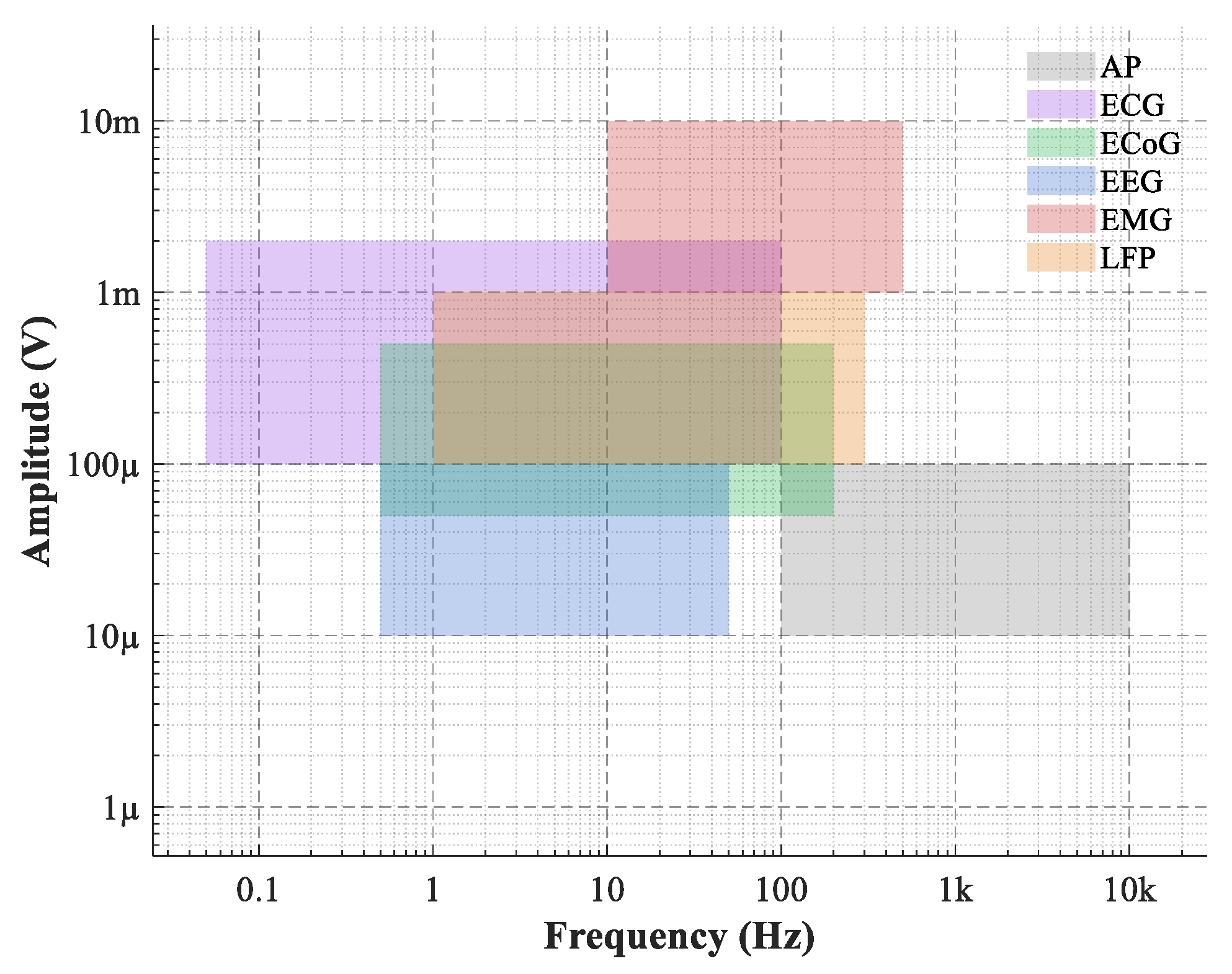
  • A relatively high ±500mV input range and a bandwidth extending up to 10 kHz enable the front-end AFE (Analog Front-End) to achieve higher amplification gain, thereby effectively reducing the system’s input-referred noise.
The remainder of this paper is organized as follows: Section 2 details the architectural innovation and circuit implementation, Section 3 presents the post-layout simulation results for the integrated circuit, and Section 4 discusses the conclusions of this work.

2. Circuit Topology

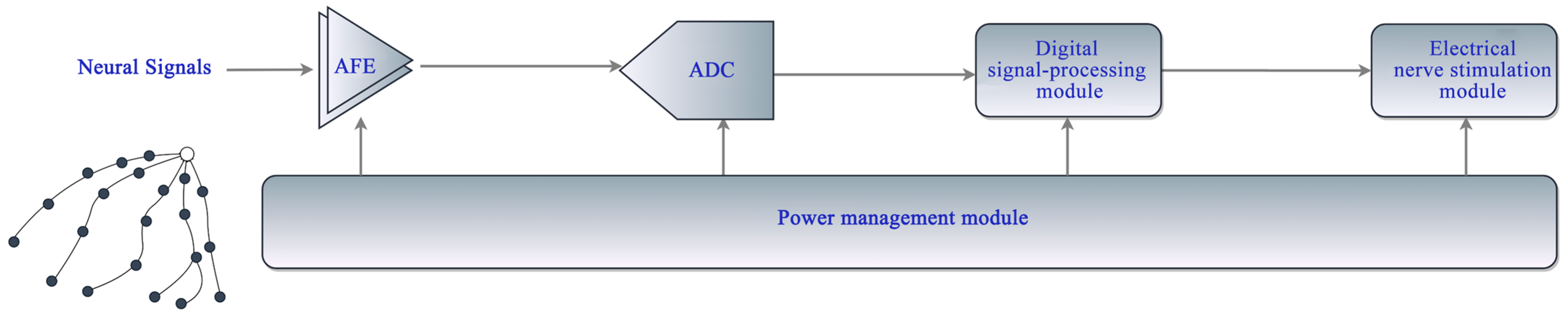
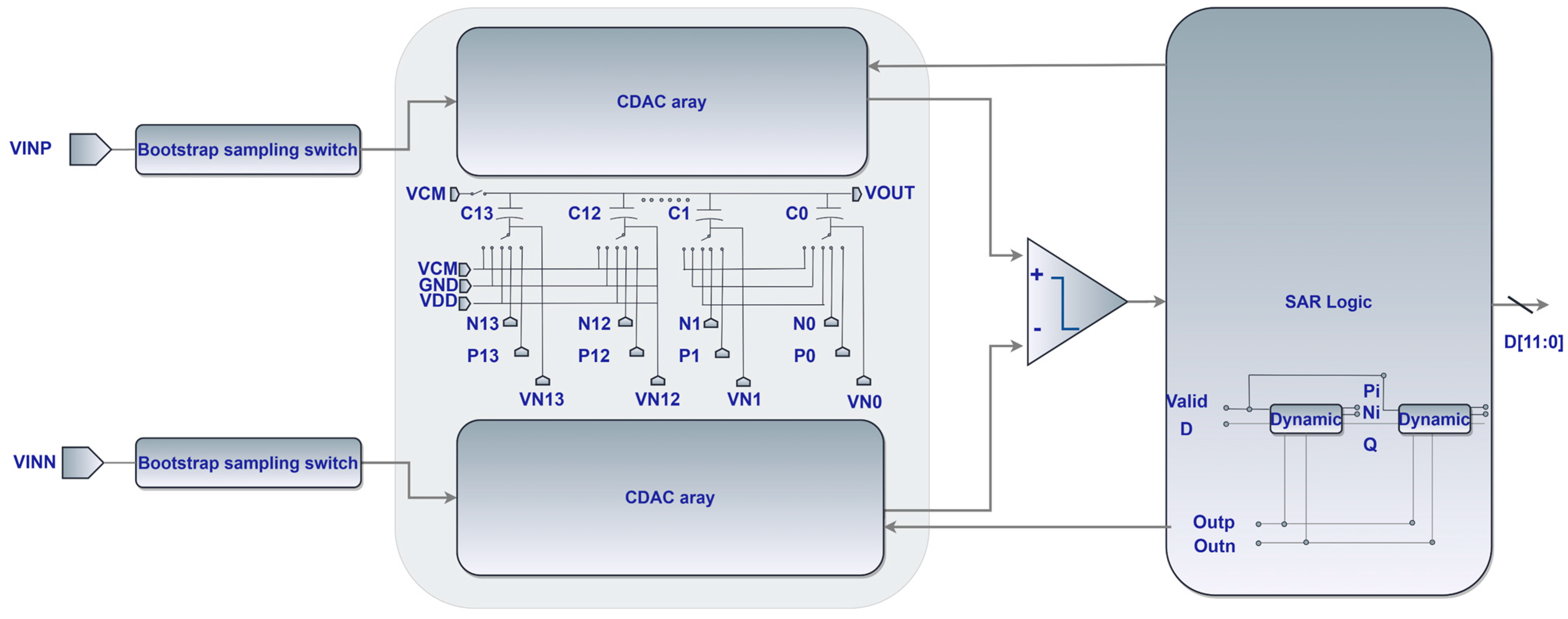
2.1. Architectural Overview

Figure 3 depicts the system architecture of the proposed SAR ADC. The circuit employs a 16 × oversampling technique. During the sampling phase, neural signals are captured using bootstrapped sampling switches and stored on the CDAC array. The SAR quantization phase involves a 12-bit successive approximation conversion, facilitated by the coordinated operation of the CDAC array, an Elzakker-type dynamic comparator, and dynamic SAR logic control.
Key functional blocks include bootstrapped sampling switches for linear signal acquisition, a segmented CDAC array with VCM-based switching to minimize power consumption, and a low-kickback Elzakker dynamic comparator to ensure high-speed and accurate decision-making. The dynamic SAR logic control unit is designed to optimize power efficiency, enabling the ADC to meet the stringent requirements of brain–computer interface applications.

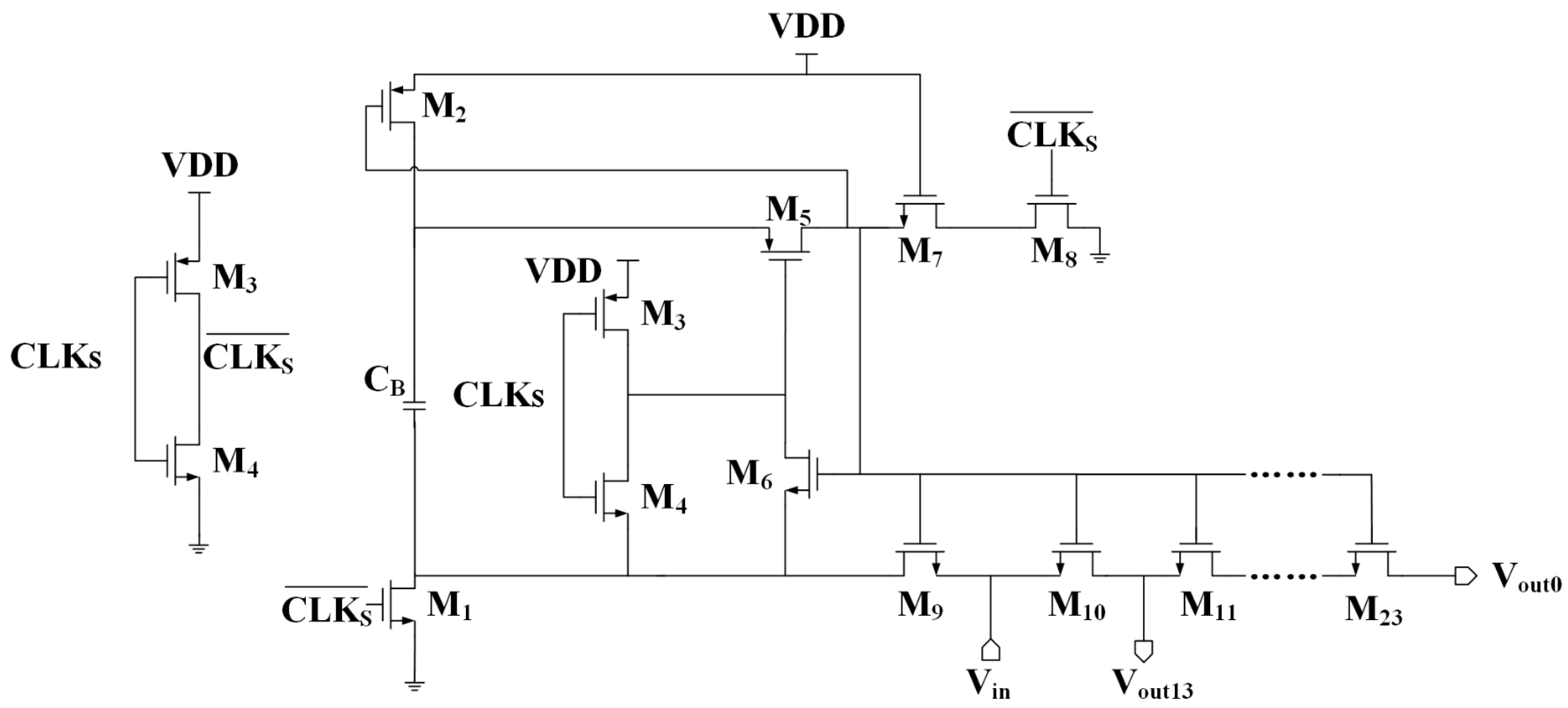
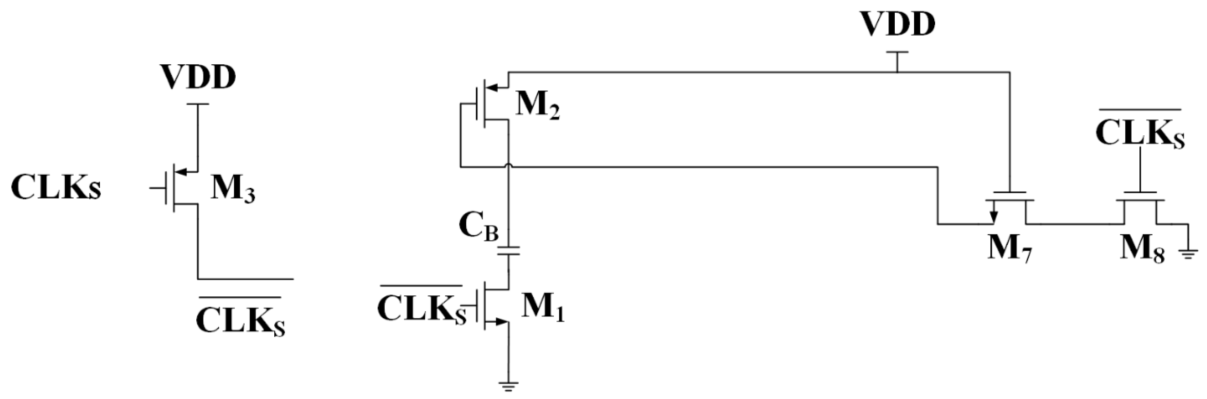
2.2. Bootstrapped Sampling Switch Design

As depicted in Figure 4, the charge-pump bootstrapped sampling circuit incorporates dynamic gate biasing technology. Compared to conventional transmission gate switches, the primary advantage of this architecture lies in its constant on-resistance (Ron): by stabilizing the gate-to-source voltage (VGS), it maintains a uniform Ron regardless of input signal amplitude variations, while simultaneously avoiding the limited input/output swing issue inherent in complementary CMOS switches and the difficulty of generating precise complementary clock signals. As illustrated in Figure 5 and Figure 6, the circuit operates in two primary phases:
  • Φ1 (Reset Phase):
The circuit enters a reset state where the top and bottom plates of the bootstrap capacitor are connected to VDD and GND, respectively. The bootstrap capacitor charges to VDD, storing the necessary charge for subsequent operation.
2.
Φ2 (Sampling Phase):
The circuit enters a pumped state, where the source terminal of the switch transistor connects to the bottom plate of the bootstrap capacitor and the gate terminal connects to the top plate of the bootstrap capacitor. Consequently, the gate-to-source voltage (VGS) is pumped to (Vin + VDD), ensuring VGS = VDD (independent of input voltage).
This implementation eliminates the inherent nonlinear Ron variation of standard CMOS switches, with its on-resistance expressed as follows:
R on , bootstrap = 1 μ n C ox W N L N V DD V THN ,
where μn represents electron mobility (a process-dependent parameter), Cox denotes the gate oxide capacitance per unit area, WN and LN correspond to the width and length of the NMOS switch transistor, VGS is the gate-to-source voltage, where VGS equals VDD., and VTHN is the threshold voltage. The critical term (VDD − VTHN) remains stabilized through the bootstrapping mechanism, ensuring immunity to input signal fluctuations.
For bootstrapped gate-voltage switch circuits, the primary sources of nonlinearity include the following:
  • The charge injection effect in switch transistors manifests when the device turns off, as the inversion layer channel charge redistributes through the source/drain terminals, inducing an error voltage ΔV on the sampled-and-held signal.
  • Clock Feedthrough Effect: when the clock signal transitions, it couples onto the sampling capacitor through the gate-drain overlap capacitance (Cgd) or gate-source overlap capacitance (Cgs) of the switch transistor, introducing nonlinear perturbations at the sampled output.
  • Body Effect (Substrate Bias Effect): in n-well processes, the body effect in NMOS switch transistors must be rigorously considered, as the threshold voltage (VTH) exhibits a nonlinear dependence on the input signal (Vin), directly contributing to sampling nonlinearity.
In addition to the aforementioned nonlinearity sources, sampling clock jitter also introduces signal distortion, as visually demonstrated in Figure 7.
δ(nT) denotes the temporal deviation between actual and ideal sampling instants at the time nT, representing clock jitter in the time domain. Δ(nT) quantifies the voltage error between the measured sample value and the ideal value at nT. The polarity of Δ(nT) is determined by the signs of δ(nT) and the input signal’s slope, where for a sinusoidal input signal x(t) = Asin(ωint), the sampling error caused by clock jitter is expressed as follows:
Δ x n T = A ω in δ n T cos ω in n T .
The random clock jitter can be modeled as a white noise source xjitter(t) that is added to the input prior to ideal sampling, where the resulting sampling error power due to clock jitter is given by the following:
x j i t t e r 2 t = [ A ω in cos ω in t ] 2 δ j i t t e r 2 t = ( 2 π f in A ) 2 2 δ j i t t e r 2 t .
Given the input sinusoidal signal power of A2/2, the resulting signal-to-noise ratio degradation caused by sampling clock jitter is as follows:
S N R j i t t e r | dB = 20 lg 2 π f in δ j i t t e r t .
The signal-to-noise ratio degradation caused by clock jitter depends not only on the jitter itself, but also on the input frequency, with empirical design practice requiring that jitter-induced noise remains below half of the quantization noise, expressed as follows:
( 2 π f in A ) 2 2 δ j i t t e r 2 t 1 2 12 ( 2 A 2 N ) 2 ,
δ j i t t e r 2 t 1 12 π 2 f in 2 2 2 N .
For a 12-bit ADC operating at 320 kS/s, the RMS jitter δjitter must be maintained at below 2.31 ns—a readily achievable specification—while the white noise introduced by clock jitter can be effectively suppressed through oversampling techniques, demonstrating how moderate-speed converters benefit from relaxed jitter requirements and noise-shaping capabilities.
According to references [12,13], the third-order harmonic distortion introduced by a constant on-resistance sampling switch is given by the following expression, indicating that linearity can be improved by reducing the on-resistance while increasing the VGS of the sampling transistor.
H D 3 1 4 A 2 V GS V TH 2 2 π f i n R C L
where A represents the input signal amplitude, fin denotes the input frequency, R is the on-resistance, and CL signifies the sampling capacitance.
The synchronous clock-controlled circuit features fixed conversion time for each bit. Through a series-connected MOSFET configuration, this design enables optimized switch transistor sizing where each bit’s capacitor employs switches with tailored on-resistance—this approach minimizes the overall device area while maintaining timing precision, as illustrated in Figure 4. The ellipsis (...) in the schematic denotes replicated MOS transistors with identical configurations.
Operating at a 320 kS/s sampling rate with a 9.6875 kHz input frequency that satisfies coherent sampling conditions, the dynamic performance characteristics of the least significant bit in the sampling circuit are demonstrated in Figure 8.

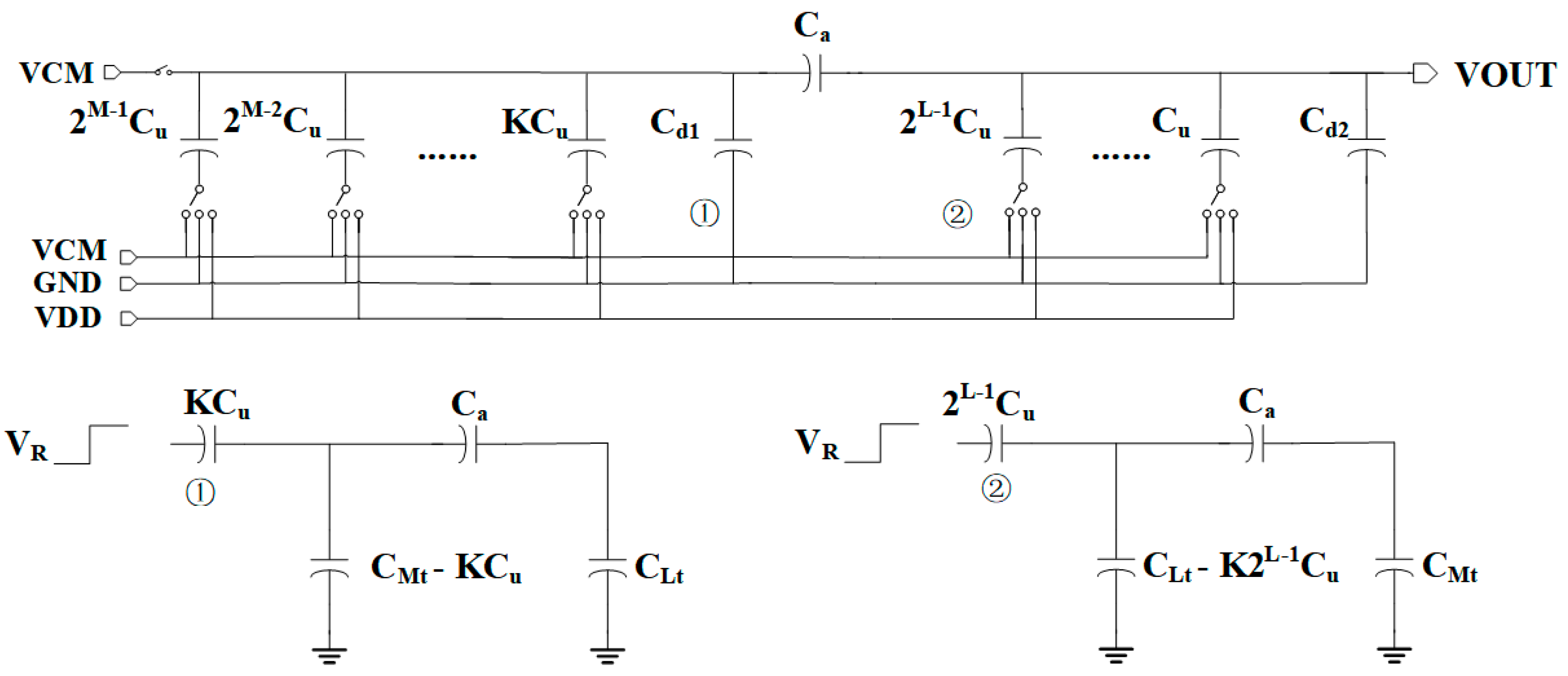
2.3. Capacitive DAC Array Design

The CDAC architecture proposed in this design is shown in Figure 9. The capacitance values in the MSB (most significant bit) section are 32 Cu, 16 Cu, 8 Cu, 4 Cu, 4 Cu, 2 Cu, and 1 Cu; those in the LSB (least significant bit) section are 32 Cu, 16 Cu, 8 Cu, 8 Cu, 4 Cu, 2 Cu, and 1 Cu. Here, Cu represents the unit capacitor. In the schematic, VN0 to VN13 denote the outputs of each stage in the preceding bootstrapped sampling switch, and N13 to N0 and P13 to P0 are signals fed back by the SAR logic array.
The CDAC architecture synergistically integrates three innovative techniques: bottom-plate sampling with a VCM reference switching protocol for charge injection cancellation, a segmented binary-weighted structure employing bridge capacitors for area-efficient impedance matching, and strategic insertion of redundant bits in both MSB and LSB sections for error correction. This optimized system architecture achieves a remarkable 87% switching energy reduction and 98.3% area savings compared to conventional implementations through novel charge redistribution pathways and switched-capacitor network optimizations.
The bottom-plate sampling technique ensures that the total charge on the capacitor’s top plate node remains constant after switch disconnection, effectively isolating the critical sampling node from charge injection and charge absorption effects during switch transitions while maintaining invariant charge conditions on the upper plate that protect comparator input pair MOSFETs from disturbance, thereby enabling the ADC to achieve a superior linearity performance through this charge-conserving architecture.
The VCM-based switching scheme incorporates an additional reference voltage at VCM = 1/2VDD = 900 mV where, during sampling, all capacitor bottom plates connect to VCM before the SAR logic array, upon completing comparison, drives each capacitor’s bottom plate to either VDD or GND based on the conversion results [14]. This methodology ensures that each capacitor switches only once per conversion cycle while maintaining a constant input common-mode voltage at the comparator through simultaneous differential capacitor switching, thereby achieving the dual advantages of power reduction during capacitor switching and a simplified comparator design by eliminating common-mode transients that would otherwise require complex auto-zeroing or offset cancellation circuitry.
The high-precision SAR ADC typically adopts a segmented capacitor array structure, as illustrated in Figure 10, where this partitioning architecture effectively reduces the number of unit capacitors needed to optimize the chip area while simultaneously lowering the performance requirements for sampling switches and accelerating the CDAC settling time through the reduced capacitive load. To ensure proper binary weighting accuracy, the smallest capacitor in the MSB array must maintain precisely twice the weight of the largest capacitor in the LSB section—this critical ratio guarantees that when applying VR step inputs at test points 1 and 2, the resulting DAC output voltage Vo exhibits correct code transition behavior meeting the d V o 1 = 2 d V o 2 relationship, and:
d V O 1 = K C u C a + C L t X V R ,
d V O 2 = 2 L 1 C a C u X V R ,
where the variables Cu, Ca, and CLt represent the unit capacitance serving as the fundamental weighting element, the bridge capacitor that couples the MSB and LSB arrays while compensating for voltage division effects, and the total LSB capacitance incorporating both designed values and parasitic components, respectively.
Hence, we derive that:
C a C u = k 2 L k C L t C u ,
C L t 2 L 1 C u ,
Simplification yields the following:
C a C u 1 , K = 1 C a C u > K , K > 1 .
The finalized bridge capacitor values under various K conditions are presented in Table 1.
Furthermore, the bridge capacitor’s value is determined solely by the parasitic capacitance associated with the LSB capacitor array while remaining independent of MSB parasitics—this critical distinction arises because the MSB parasitic components merely introduce a constant charge offset that uniformly scales the DAC’s gain factor without affecting code-to-code transition linearity, whereas LSB parasitics directly modify the inter-segment charge division ratio and, thus, must be explicitly compensated through careful bridge capacitor sizing to maintain the required Ca/CLt proportionality that ensures monotonic step progression.
The incorporation of redundancy effectively corrects comparator decision errors typically caused by four key factors: parasitic resistance and inductance in power/ground routing that induce supply voltage ripple, the limited driving capability of the VREF buffer, the excessive settling time from large RC time constants in the CDAC capacitor switch network, and intrinsic comparator noise. This redundancy creates multiple digital code representations for single analog values (e.g., value 4 mapping to both 01000 and 00111 codes) through strategically allocated decision threshold overlap, thereby establishing error tolerance margins that absorb timing uncertainties and noise-induced metastability while maintaining conversion accuracy. In the CDAC array of this design with redundancy insertion, the redundancy allocation per bit is tabulated as shown in Table 2.
The unit capacitance Cu in the CDAC is bound by two critical factors:
  • kT/C noise constraint
The quantization noise of an ADC must exceed its sampling thermal noise.
k T C u n i t V R E F 2 12 · 2 2 N C u n i t 12 · 2 24 k T V R E F 2 = 96.4   fF .
2.
Capacitor mismatch
Process variations and parasitic capacitance introduced during the layout design inevitably cause capacitor mismatch. The maximum standard deviation of integral nonlinearity (INL) in the ADC is given by the following:
σ INL , max = 2 N 1 σ u Cu LSB .
The maximum allowable standard deviation of integral nonlinearity ( σ INL , max ) in an ADC must satisfy the following:
3 σ I N L , m a x = 3 2 N 1 σ u C u L S B < 0.5 L S B .
Simplification yields:
σ u C u < 1 6 2 N 1 .
Solving the equation yields:
σ u C u < 0.37 % .
The process library’s MIM (Metal–Insulator–Metal) capacitor with a minimum value of 127.36 fF demonstrates a 0.22% mismatch (ΔC/C) under Monte Carlo simulation, as illustrated in Figure 11, comfortably meeting the matching requirement for high-precision analog design.

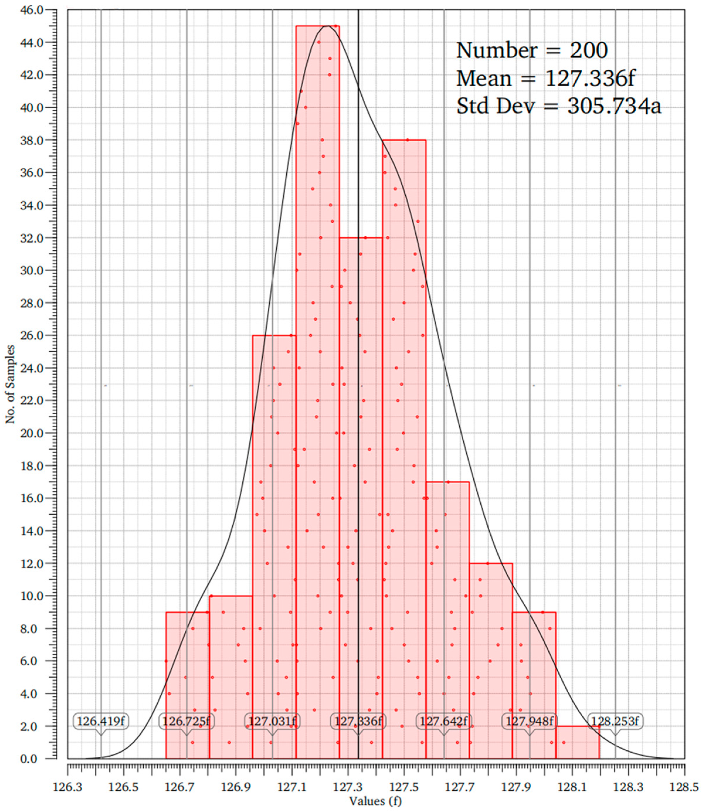
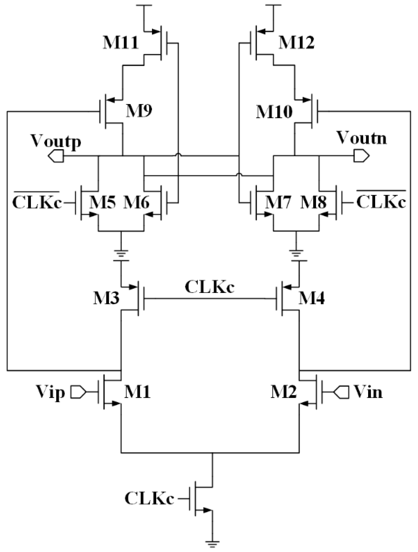
2.4. Dynamic Comparator Design

The conventional StrongARM latch employs a single-stage topology, delivering rapid response times and zero static power consumption for inherently low-power operation [15]. However, the stacked configuration of the latch and input pair introduces severe kickback noise—the complementary output transitions directly couple to the input nodes through the CGS of the input transistors, creating significant signal disturbance that degrades sampling accuracy in high-resolution ADCs [16].
The double-tail architecture decouples the preamplifier stage from the latch, significantly reducing kickback noise through two-stage isolation—yet it incurs higher power consumption as both differential load capacitors in the preamp stage discharge fully from VDD to GND during each comparison cycle.
The adopted Elzakker architecture, as illustrated in Figure 12, improves upon the double-tail design by inserting cross-coupled PMOS pairs (M9, M10) in the latch stage while eliminating the tail current source, achieving direct power savings through two key mechanisms [17]:
  • Static Current Elimination
The proposed design eliminates the constant tail current dissipation characteristic of conventional double-tail latches, converting the structure into a fully dynamic implementation with zero static power consumption.
2.
Controlled Regeneration
PMOS pairs M9/M10 accelerate decision-making during metastability, reducing dead-zone time by 30% versus passive loads. This maintains kickback isolation (comparable to double-tail) via retained preamp decoupling.
The operational sequence begins with the reset phase, where M9/M10 precharge internal nodes. In the evaluation phase, the input differential modulates the preamp outputs. Finally, during the regeneration phase, cross-coupled inverters resolve the digital level.
The designed comparator circuit achieves a 0.12 μs resolution time for discriminating 0.12 mV (½LSB @12-bit) signals, with Cadence Virtuoso transient noise simulations verifying an input-referred noise of 69.5 μV RMS—meeting the critical requirements for a 12-bit SAR ADC operating at 320 kS/s. Key validation results include the following:
  • Noise Compliance
The measured 69.5 μV noise, representing 0.58 × LSB (where LSB = 120 μV at 1 V range), ensures quantization-limited performance, with its composition dominated by the input pair thermal noise (~60%) and latch metastability-induced uncertainty (~40%).
2.
Monte Carlo Offset Analysis
As illustrated in Figure 13, the simulated offset voltage exhibits 3σ < 0.5LSB (120 μV), achieved through large input devices for mismatch reduction and auto-zeroing during the reset phase.
3.
Speed–Noise–Power Tradeoff
A delay of 0.12 μs ensures a 16× oversampling margin for 320 kS/s operation and consumes 8.982 μW @1.8 V, optimized via dynamic bias control.

2.5. SAR Logic Array Design

The proposed SAR control logic utilizes dynamic circuit techniques to enhance power efficiency, differing from conventional implementations such as ring counters with shift registers (static CMOS) or N flip-flops with combinational logic. As illustrated in Figure 14, this design incorporates event-driven operation that activates only during comparison phases, a dynamic latch array to store comparator decisions until the next reset, and non-overlapping clock control to prevent shoot-through currents.
The timing diagram of the SAR dynamic logic unit operation is shown in Figure 15. During the sampling phase, when the D signal remains at a low logic level and the Valid signal transitions to a high logic state, the CLK signal asserts a high logic level, thereby pulling the voltage at node Q to ground potential. In this configuration, both the positive input (Pi) and negative input (Ni) of the comparator remain at low logic levels, causing the comparator’s differential outputs Outn (negative output) and Outp (positive output) to settle in high-logic states. During the quantization phase, the Sample signal transitions to low logic, while the Valid signal remains highly asserted during the comparator’s comparison phase. The CLK voltage is discharged to low logic through transistors M2 and M3. Upon completion of the comparator’s comparison operation, one of the differential outputs (Outn or Outp) transitions to low logic. If Outn is driven to low logic, transistor M9 is activated, charging the Pi node to high logic, while the Ni node retains its low logic state. When the Pi node transitions to high logic, transistors M14 and M8 are activated, further charging the Pi node and discharging the Ni node, thereby latching the current comparison result. Subsequently, regardless of changes in the comparator’s outputs, the latched result remains stable until a reset signal assertion occurs. During the reset phase of the comparator, the Valid signal is de-asserted (transitioning to low logic). The voltage at node Q is charged to high logic through transistors M4 and M5. This high-logic state at node Q propagates to the subsequent logic gate, triggering a state transition in the downstream circuitry, thereby ensuring that each comparison result is latched.
The circuit augments the conventional architecture by integrating two bypass MOSFETs (M8 and M11) and two additional inverters. Upon the comparator’s decision, this configuration enables faster result latching, relaxes the requirements for enabling signal transmission circuitry, and mitigates logic errors.
Compared to static implementations, this architecture significantly reduces clock network power, decreases control signal fan-out, and minimizes parasitic capacitance at critical nodes. The absence of continuous DC paths and reduced switching activity collectively enable sub-μW power consumption while ensuring robust metastability handling.

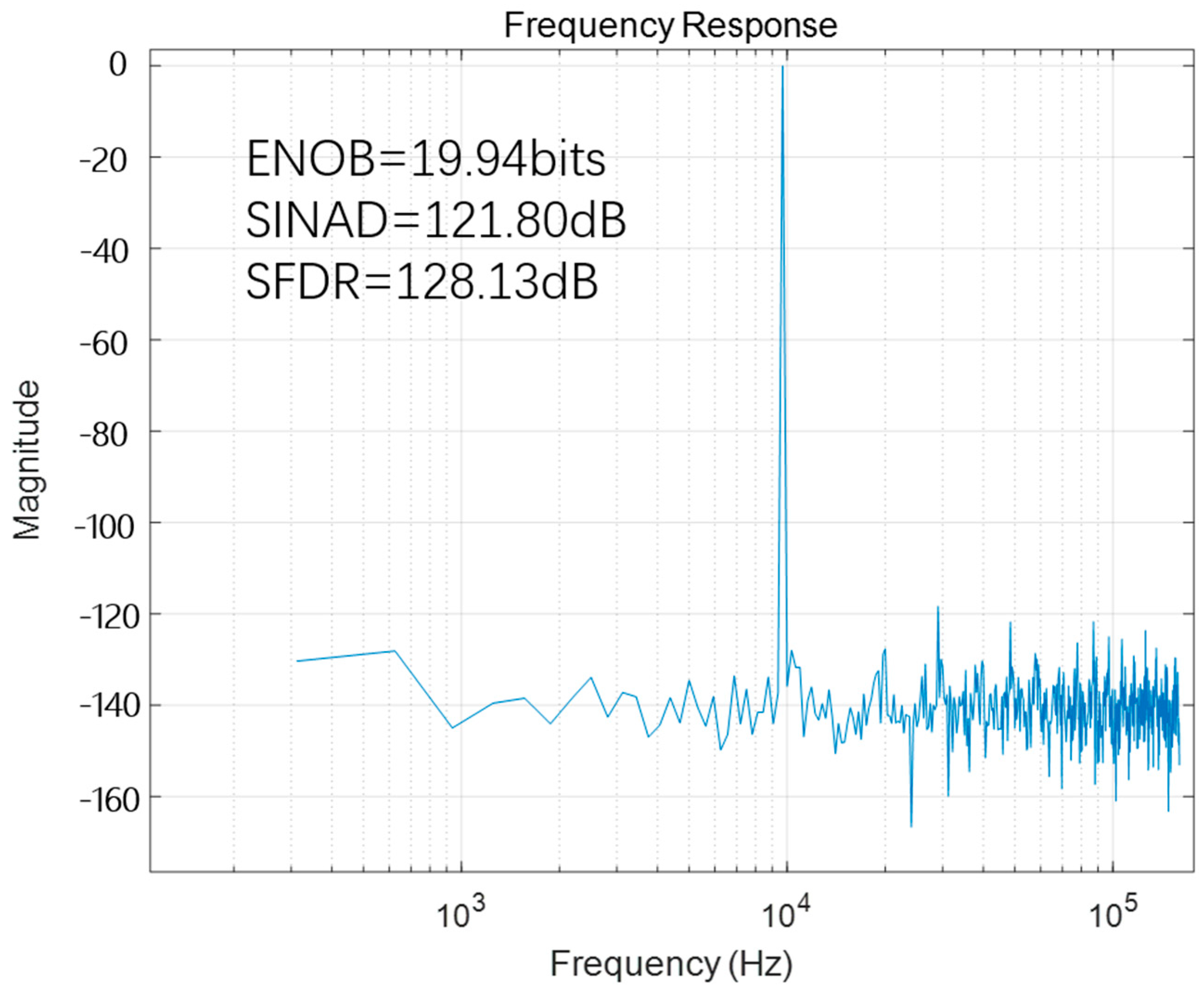
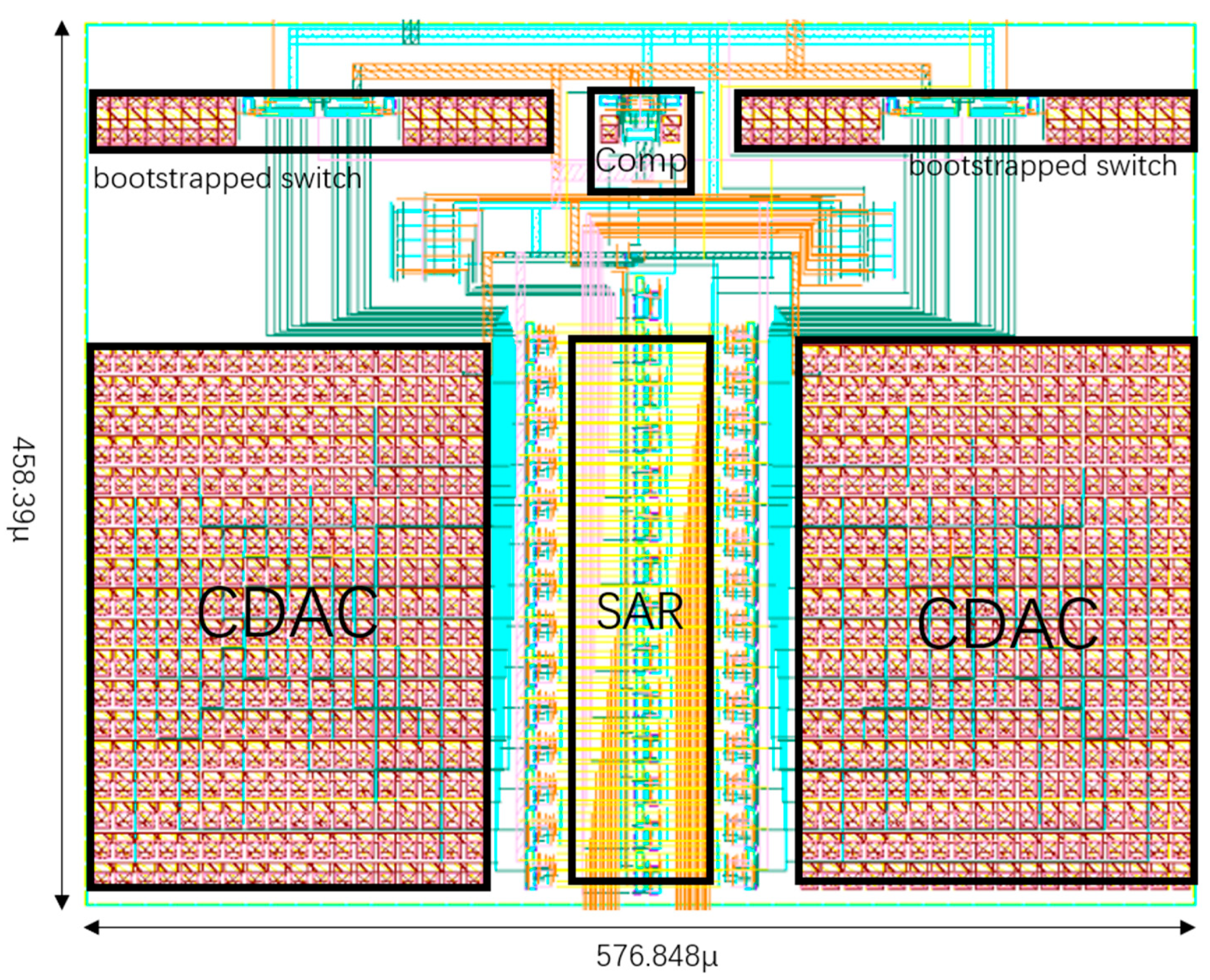
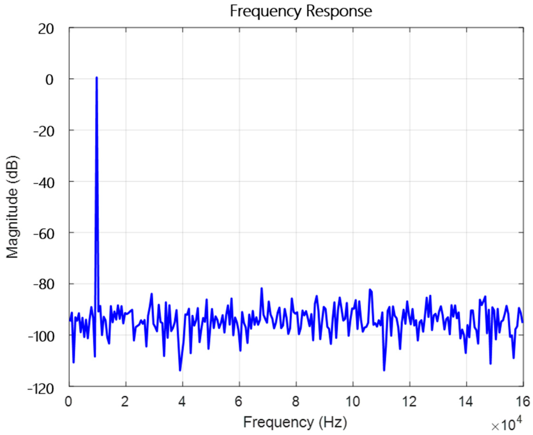
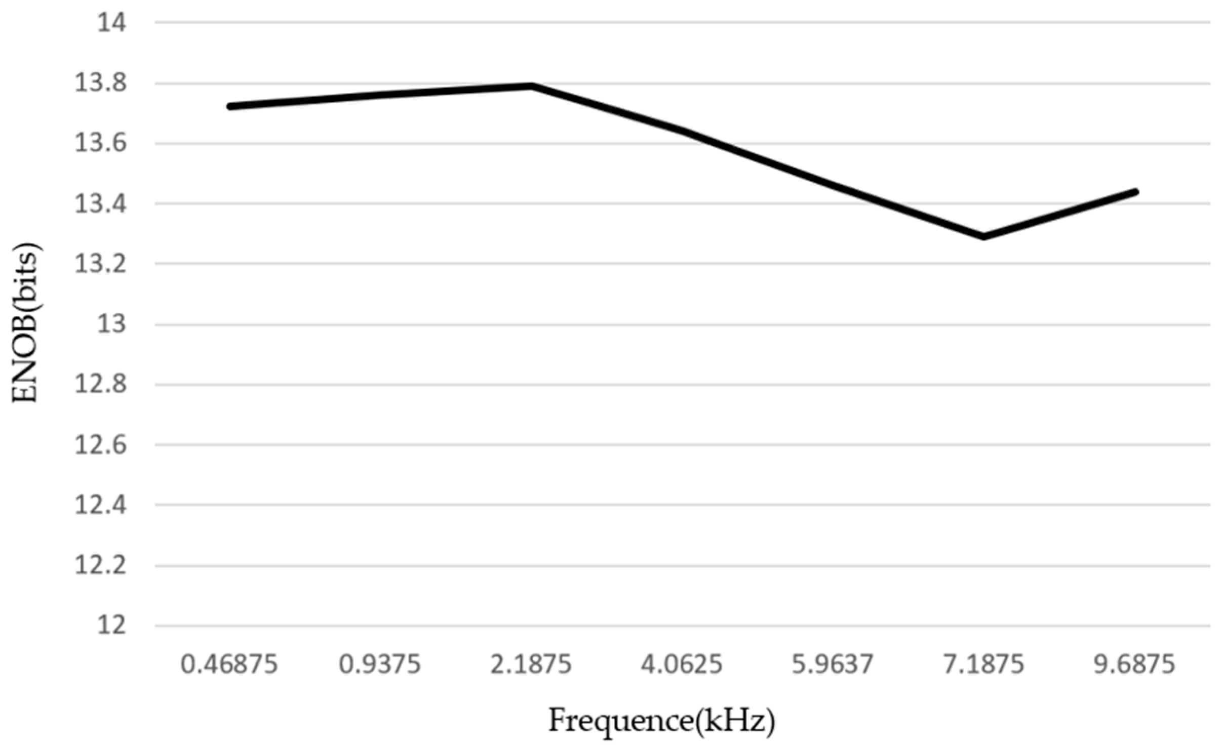
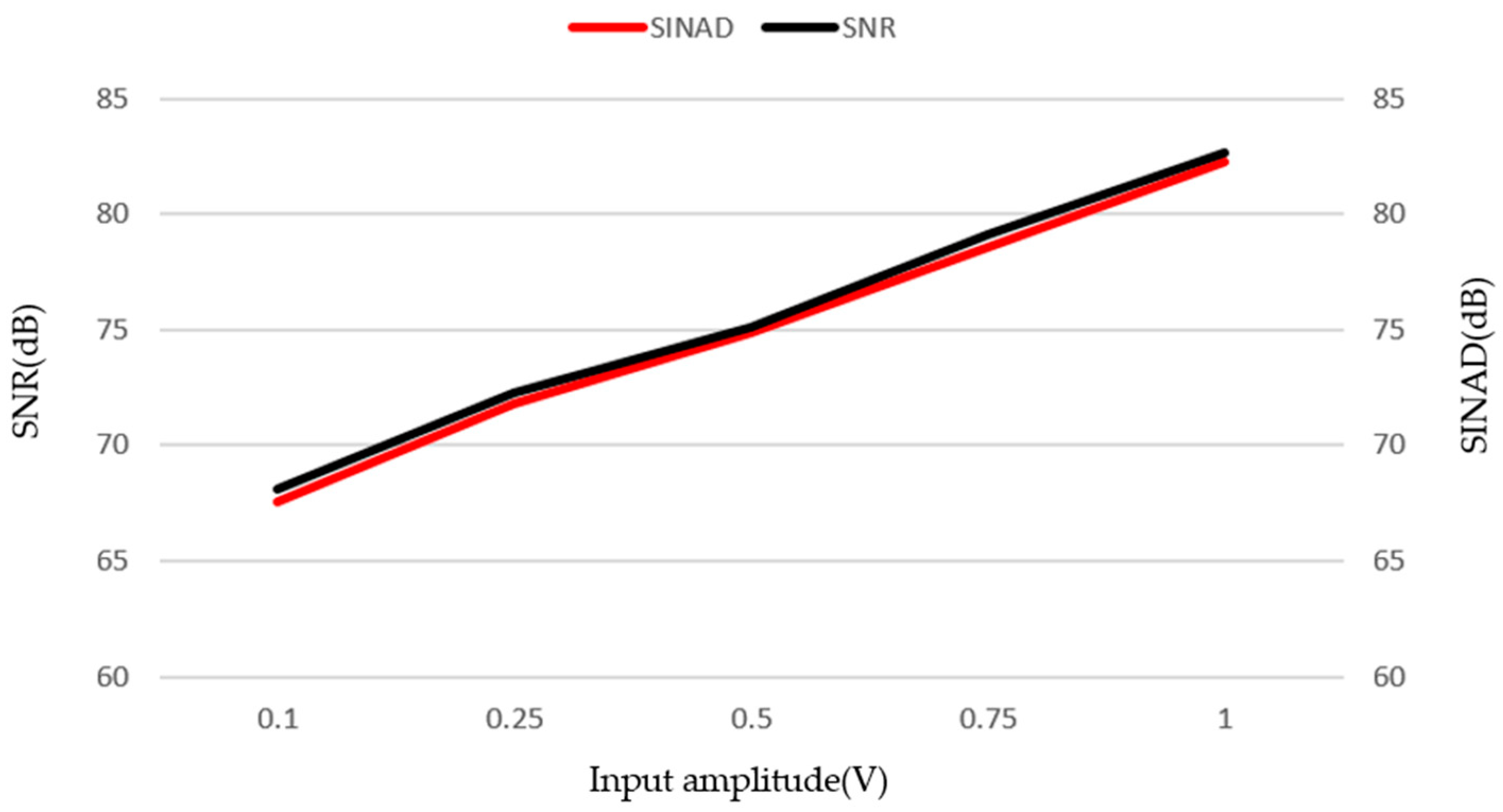
3. Layout Implementation and Post-Layout Simulation Results

The proposed SAR ADC was designed using 180 nm CMOS technology, achieving a compact core area of 0.2475 mm2 through meticulous layout optimization. Figure 16 illustrates the symmetrical floorplan with capacitor arrays distributed across the left–right peripheries, while the central placement of critical analog modules—including bootstrapped switches, dynamic comparators, and unity-gain buffers—minimizes interconnected parasitics. The SAR logic block is strategically positioned adjacent to the capacitive DAC array to reduce switching noise coupling. Analog signal routing employs current-density optimized traces (4 mA/μm width) with differential symmetric paths, maintaining a <5% length mismatch through careful metal layer planning. Proximity grouping of the comparator, sampling switches, and CDAC array achieves effective mitigation of RC delay variations.
As illustrated in Table 3, the SAR ADC developed in this study exhibits remarkable performance metrics tailored for BCI applications, demonstrating superior precision and energy efficiency, as well as dynamic characteristics essential for high-fidelity acquisition of weak biological signals. The design achieves an ENOB of 13.44 bits, surpassing traditional SAR ADCs (e.g., 11.12 bits in [18]) and CT-DSM architectures (9.62 bits), thereby minimizing quantization-induced distortion. Under coherent sampling conditions (Fin = 9.6875 kHz, Fs = 320 kS/s), the ADC demonstrates a SINAD of 82.67 dB and an SFDR of 89.62 dB, as illustrated in Figure 17. The performance sweep results of ENOB and SNR as they vary with input frequency are shown in Figure 18, and the results of SNR and SINAD as they vary with input amplitude are shown in Figure 19, further validating SAR ADC’s capability to maintain high signal integrity and suppress harmonic distortion in real-world operating scenarios.
From a power efficiency perspective, the proposed SAR ADC consumes only 27.9 µW, significantly less than comparable designs (e.g., 40.5 µW in [19]), and is substantially more efficient than IADC2-1 (2.95 mW) [20]. Detailed power analysis reveals that the comparator dominates power consumption at 8.982 μW (32.1% of the total), followed by CDAC switching at 8.946 μW (32.0%), clock distribution at 9.0936 μW (32.5%), and SAR logic at 0.936 μW (3.3%). This optimized power distribution ensures efficient energy utilization, which is critical for extending the operational lifetime of implantable devices and meeting the stringent energy constraints of long-term BCI monitoring. Additionally, the ADC’s bandwidth of 10 kHz accommodates the full spectrum of neural signals (0.5–5 kHz) while supporting higher-frequency signal acquisition, such as electromyographic data or motion artifact monitoring, thereby enhancing system versatility.
Considering the LDO (Low-Dropout Regulator) required for subsequent on-board testing, the circuits designed in this project all operate with a 1.8 V supply voltage, similar to those described in references [19,21], so the requirements for the LDO are quite comparable. Compared to the LDO in [19], this design may have slightly higher power consumption, though it will remain significantly lower than the power consumption reported in [20]. Except for reference [18], which mentions an input capacitance of 2 pF, other references do not provide detailed descriptions of this parameter. Reference [18] uses MOM (Metal–Oxide–Metal) capacitors, where the size of the unit capacitor is 1 pF. Such a small capacitor may introduce the risk of capacitor mismatch. Since the minimum capacitor available in the process library used for this design is a MIM (Metal–Insulator–Metal) capacitor with a value of 127.36 fF, the input capacitance of the circuit is 17 pF. Comparison shows that the area utilization efficiency of the CDAC in this paper is significantly higher than that of the CDAC structure in reference [18]. Compared to the design in [18], this may require the preceding AFE (Analog Front-End) to have stronger driving capability and consume more power.
Designed and post-layout-simulated using a 180 nm process, the proposed SAR ADC benefits from compatibility with established biomedical chip manufacturing technologies, reducing production costs and facilitating integration into multi-channel systems. Moreover, it outperforms traditional SAR ADCs (e.g., the 11.12-bit ENOB in [21]) in terms of resolution, dynamic range, and power consumption, addressing the critical requirements of high-precision neural signal processing. In conclusion, the proposed SAR ADC, through its optimized architecture and circuit design, delivers high resolution and a dynamic performance while maintaining ultra-low power consumption, positioning it as a robust option for long-term implantable monitoring and high-accuracy signal acquisition in BCI systems, with significant potential for widespread adoption in biomedical applications.

4. Conclusions

This paper presents a low-power, high-resolution SAR ADC tailored for BCI systems. Leveraging a segmented monotonic switching scheme, dynamic logic architecture, and an optimized CDAC, the design achieves a 13.44-bit ENOB and 27.9 μW of power consumption at a supply voltage of 1.8 V, with a compact core area of 0.24 mm2. The experimental results demonstrate an SNDR of 81.94 dB and an SFDR of 91.69 dBc at a sampling rate of 320 kS/s, making it well suited for neural signal acquisition and biomedical sensing applications. While the 180 nm CMOS process imposes limitations on voltage scaling and current leakage reduction, the design maintains a competitive performance in power efficiency and area optimization. Future work, including process migration to advanced nodes and further circuit-level enhancements, is expected to extend SAR ADC’s applicability to implantable medical devices and portable instrumentation.

Author Contributions

Conceptualization, H.Y.; Methodology, H.Y.; Software, H.Y.; Validation, H.Y.; Formal analysis, H.Y.; Investigation, H.Y.; Resources, H.Y.; Data curation, H.Y.; Writing—original draft, H.Y.; Writing—review & editing, H.Y. and J.C.; Visualization, H.Y.; Supervision, J.C.; Project administration, J.C.; Funding acquisition, C.L. All authors have read and agreed to the published version of the manuscript.

Funding

This research is supported by Lingang Laboratory through Key Project LG-GG-202402-05-02.

Institutional Review Board Statement

Not applicable.

Informed Consent Statement

Not applicable.

Data Availability Statement

The data presented in this study are available on request from the corresponding author. The data are not publicly available because the research is supported by Lingang Laboratory.

Conflicts of Interest

Author Jiahao Cheong was employed by the company MTRIX. The remaining authors declare that the research was conducted in the absence of any commercial or financial relationships that could be construed as a potential conflict of interest.

References

  1. Jeong, K.; Ha, S.; Je, M. A 15.4-ENOB, Fourth-Order Truncation-Error-Shaping NS-SAR-Nested ΔΣ Modulator With Boosted Input Impedance and Range for Biosignal Acquisition. IEEE J. Solid-State Circuits 2023, 59, 528–539. [Google Scholar] [CrossRef]
  2. Shah, S.A.A.; Zhang, L.; Bais, A. Dynamical system based compact deep hybrid network for classification of Parkinson disease related EEG signals. Neural Netw. 2020, 130, 75–84. [Google Scholar] [CrossRef] [PubMed]
  3. Koller-Schlaud, K.; Ströhle, A.; Bärwolf, E.; Behr, J.; Rentzsch, J. EEG Frontal Asymmetry and Theta Power in Unipolar and Bipolar Depression. J. Affect. Disord. 2020, 276, 501–510. [Google Scholar] [CrossRef] [PubMed]
  4. Eldele, E.; Chen, Z.; Liu, C.; Wu, M.; Kwoh, C.-K.; Li, X.; Guan, C. An attention-based deep learning approach for sleep stage classification with single-channel EEG. IEEE Trans. Neural Syst. Rehabil. Eng. 2021, 29, 809–818. [Google Scholar] [CrossRef] [PubMed]
  5. Wang, X.; Zhang, J.; He, C.; Wu, H.; Cheng, L. A Novel Emotion Recognition Method Based on the Feature Fusion of Single-Lead EEG and ECG Signals. IEEE Internet Things J. 2023, 11, 8746–8756. [Google Scholar] [CrossRef]
  6. Chen, M.; Chun, H.S.; Castro, I.D.; Torfs, T.; Lin, Q.; van Hoof, C.; Wang, G.; Lian, Y.; van Helleputte, N. A 400 GΩ Input-Impedance Active Electrode for Non-Contact Capacitively Coupled ECG Acquisition With Large Linear-Input-Range and High CM-Interference-Tolerance. IEEE Trans. Biomed. Circuits Syst. 2019, 13, 376–386. [Google Scholar] [CrossRef] [PubMed]
  7. Casson, A.J.; Saunders, R.; Batchelor, J.C. Five day attachment ECG electrodes for longitudinal bio-sensing using conformal tattoo substrates. IEEE Sens. J. 2017, 17, 2205–2214. [Google Scholar] [CrossRef]
  8. Cogan, S.F. Neural stimulation and recording electrodes. Annu. Rev. Biomed. Eng. 2008, 10, 275–309. [Google Scholar] [CrossRef] [PubMed]
  9. Jie, L.; Tang, X.; Liu, J.; Shen, L.; Li, S.; Sun, N.; Flynn, M.P. An Overview of Noise-Shaping SAR ADC: From Fundamentals to the Frontier. IEEE Open J. Solid-State Circuits 2021, 1, 149–161. [Google Scholar] [CrossRef]
  10. Boni, A.; Giuffredi, L.; Pietrini, G.; Ronchi, M.; Caselli, M. A low-power Sigma-Delta modulator for healthcare andmedical diagnostic applications. IEEE Trans. Circuits Syst. I Regul. 2021, 69, 207–219. [Google Scholar] [CrossRef]
  11. Zheng, Z.; Wei, L.; Lagos, J.; Martens, E.; Zhu, Y.; Chan, C.H.; Craninckx, J.; Martins, R.P. 163 A single-channel 5.5 mW 3.3 GS/s 6b fully dynamic pipelined ADC with post-amplification residue generation. In Proceedings of the 2020 IEEE Intemational SolidState Circuits Conference-(ISSCC), San Francisco, CA, USA, 16–20 February 2020; IEEE: Piscataway, NJ, USA, 2020; pp. 254–256. [Google Scholar]
  12. Yu, W.; Sen, S.; Leung, B. Distortion analysis of MOS track-and-hold sampling mixers using time-varying Volterra series. IEEE Trans. Circuits Syst. II Analog. Digit. Signal Process. 1999, 46, 101–113. [Google Scholar] [CrossRef]
  13. Razavi, B. Principles of Data Conversion System Design; Wiley: New York, NY, USA, 1995; pp. 7–28. [Google Scholar]
  14. Zhu, Y.; Chan, C.H.; Chio, U.F.; Sin, S.W.; Martins, R.P.; Maloberti, F. A 10-Bit 100-MS/s Reference-Free SAR ADCin 90 nm CMoS. IEEE J. Solid-State Circuits 2010, 45, 1111–1121. [Google Scholar] [CrossRef]
  15. Kobayashi, T.; Nogami, K.; Shirotori, T.; Fujimoto, Y.; Watanabe, O. A current-mode latch sense amplifier and a staticpower saving input buffer for low-power architecture. In 1992 Symposium on VLSI Circuits Digest of Technical Papers; IEEE: Piscataway, NJ, USA, 1992; pp. 28–29. [Google Scholar]
  16. Razavi, B. The strongarm latch [a circuit for all seasons]. IEEE Solid-State Circuits Mag. 2015, 7, 12–17. [Google Scholar] [CrossRef]
  17. Schinkel, D.; Mensink, E.; Klumperink, E.; Van Tuijl, E.; Nauta, B. A doubletail latchtype voltage sense amplifier with 18ps setuphold time. In Proceedings of the 2007 IEEE International SolidState Circuits Conference Digest of Technical Papers (ISSCC), San Francisco, CA, USA, 11–15 February 2007; p. 314605. [Google Scholar]
  18. Chung, Y.-H.; Kuo, J.-H. A 12b Dual-Mode SAR ADC for Bio-Medical Applications. In Proceedings of the 2024 IEEE Biomedical Circuits and Systems Conference (BioCAS), Xi’an, China, 28–30 April 2024; pp. 1–5. [Google Scholar] [CrossRef]
  19. Kumaradasan, D.; Kar, S.K.; Sarkar, S. An 8-bit 1 MS/s Low-Power SAR ADC with an Enhanced EPC for Implantable Medical Devices. In Proceedings of the 2024 IEEE Computer Society Annual Symposium on VLSI (ISVLSI), Knoxville, TN, USA, 1–3 July 2024; pp. 9–14. [Google Scholar] [CrossRef]
  20. Tiwari, V.; Batra, C.; Nagaria, R. KLow power SAR ADC for bio-medical application. In Proceedings of the 2024 International Conference on Integrated Circuits, Communication, and Computing Systems (ICIC3S), Una, India, 8–9 June 2024; pp. 1–3. [Google Scholar] [CrossRef]
  21. Gao, Z.; Wang, S.; Chen, M. A 32-bit Two-step Incremental-ADC with 125.6 dB Dynamic-range for Non-invasive BCI Applications. In Proceedings of the 2024 IEEE Asia Pacific Conference on Circuits and Systems (APCCAS), Taipei, Taiwan, 7–9 November 2024; pp. 566–570. [Google Scholar] [CrossRef]
Figure 1. Bioelectric signal frequency–amplitude ranges.
Applsci 15 05494 g001
Figure 2. BCI system.
Applsci 15 05494 g002
Figure 3. System architecture of proposed SAR ADC.
Applsci 15 05494 g003
Figure 4. Charge-pump bootstrapped sampling circuit.
Applsci 15 05494 g004
Figure 5. Circuit operation during Φ1 phase.
Applsci 15 05494 g005
Figure 6. Circuit operation during Φ2 phase.
Applsci 15 05494 g006
Figure 7. Sampling under clock jitter conditions.
Applsci 15 05494 g007
Figure 8. Frequency characteristics of bootstrap switching circuits.
Applsci 15 05494 g008
Figure 9. Circuit of proposed CDAC.
Applsci 15 05494 g009
Figure 10. Segmented CDAC architecture.
Applsci 15 05494 g010
Figure 11. Monte Carlo simulation results of unit capacitors.
Applsci 15 05494 g011
Figure 12. Circuit of proposed Elzakker-type dynamic comparator.
Applsci 15 05494 g012
Figure 13. Monte Carlo simulation of comparator offset voltage.
Applsci 15 05494 g013
Figure 14. Circuit of proposed dynamic logic unit.
Applsci 15 05494 g014
Figure 15. SAR dynamic logic unit timing operation.
Applsci 15 05494 g015
Figure 16. Layout of designed circuit.
Applsci 15 05494 g016
Figure 17. FFT analysis results of post-layout circuit simulation.
Applsci 15 05494 g017
Figure 18. ENOB vs. frequency.
Applsci 15 05494 g018
Figure 19. SNR vs. input amplitude and SINAD vs. input amplitude.
Applsci 15 05494 g019
Table 1. Capacitor selection methodology for different K values.
K C a / C u C L t
112L − 1The parasitic capacitance at the LSB node, C d 2 = 0 .
122 × (2L − 1)The parasitic capacitance at the LSB node, C d 2 = 2L − 1.
144 × (2L − 1)The parasitic capacitance at the LSB node, C d 2 = 3 × (2L − 1).
242 × (2L − 2)The parasitic capacitance at the LSB node, C d 2 = 2L – 3.
Table 2. Redundancy per bit.
C13C12C11C10C9C8C7C6C5C4C3C2C1C0
Weight accumulation result2048102451225625612864321688421
Weight accumulation result of LSB23111287775519263135713923157310
Redundancy (LSB)2642642642648888880000
Table 3. Simulation performance summary and comparison with state-of-the-art systems.
[18][19][20][21]This Work
TopologyIADC2-1SARSARSARSAR
Process (nm)18090180180180
Sampling frequency (Hz)768 k20 M1 k1 M320 k
Supply (V)51.80.5/11.81.8
Power (W)2.95 m31.6 μ35.9 μ40.5 μ27.9 μ
Peak input (V)-500 m1-1
Bandwidth (Hz)0.5 k1.25 M5 k50 k10 k
Resolution (bits)32512814
ENOB (bits)18.164.5311.127.713.44
SINAD (dB)111.12968.748.1582.67
SFDR (dBc)--8355.5289.62
Disclaimer/Publisher’s Note: The statements, opinions and data contained in all publications are solely those of the individual author(s) and contributor(s) and not of MDPI and/or the editor(s). MDPI and/or the editor(s) disclaim responsibility for any injury to people or property resulting from any ideas, methods, instructions or products referred to in the content.

