1. Introduction
The assessment of the quality of insulation materials is of significant importance in modern technology. It is very important, for example, in the energy industry and automotive technology. The quality of insulation determines the trouble-free operation of electrical installations and devices, as well as the safety of their use, which is very important [
1,
2,
3].
Various indicators are used to assess the quality of electrical insulation materials. One of them is the dielectric loss factor tan δ. The dielectric loss factor is a relative quantity defined for real capacitors filled with dielectric material, and an insulating system can generally be treated in this way. This coefficient is determined as the ratio of the power losses in the tested capacitor to the power stored in it. In typical electrical insulation systems, values from 10−1 to 10−5 are required, which means that power losses in insulation are range from fractions of a percent to as much as 10%. In assessments of the quality of insulation, the value of the dielectric loss coefficient itself is less important; the changes in this coefficient are more important, indicating the degradation in insulation of the tested device or installation. In the measurement of the dielectric loss factor, high requirements for measurement accuracy are not set.
It can be seen that the dielectric loss factor is the tangent of a certain phase angle, by which the phase shift angle between the voltage and current of the tested capacitor decreases due to the flow of the active component of the current through it. For this reason, the dielectric loss factor is often referred to as tan δ.
Analog and digital measurement methods are used to measure tan δ. Its value is also a relation of the corresponding impedance components [
4,
5,
6,
7,
8,
9].
Measurement circuits require the tested object to be supplied with a voltage or sinusoidal current. The measurement signals are the voltage and current of the object being tested. These signals are generally processed in non-zero or zero measurement circuits. In non-zero circuits, the output non-zero signal of the circuit is a function of the measured parameters, while in zero circuits, the circuit is driven to the equilibrium state, which usually means reaching the zero value of the selected signal, and then the values of the measured quantities are determined on the basis of the parameters of the measurement circuit. An example of such circuits are balanced bridge circuits [
4,
5,
6,
7].
Bridges and other zero systems can measure tan δ directly. One of the most popular bridge circuits, designed to directly measure the dielectric loss factor, is the Schering bridge [
4,
5]. The power relation defining tan δ can also indirectly be determined as an impedance component relation. Bridges are also being built, in which some of the bridge elements are replaced with digital elements. Such bridges are called digital bridges [
10,
11,
12,
13,
14,
15,
16]. In all cases of zero methods, the problem is the so-called bridge’s convergence. It is the result of the bridge balancing process, which minimizes the output signal by means of successive alternating settings of the control elements. This process can be long-lasting and sometimes completely prevent the bridge from being balanced.
Measurement circuits often use the digital processing of measurement signals to measure impedance components [
8,
9,
10,
11,
12,
13,
14]. Signal processing is sometimes carried out in the form of electronic circuits and in the form of a software chain of measurement signal processing. The measurement algorithm performs operations that are equivalent to electrical connections between blocks of measurement circuits. Such implementations are called virtual instruments. For the design of virtual instruments, software packages can be used, which significantly facilitate modeling, simulations, and, finally, testing of the measurement circuit [
17].
Circuits for measuring impedance components are usually easy to digitize. Operations on measurement signals are not complicated, and changing the parameters of the system is easy. However, some difficulties may be caused by the need to derive the equations for the processing of circuits.
2. Bridge with Modular Balancing for Dielectric Loss Factor Measuring
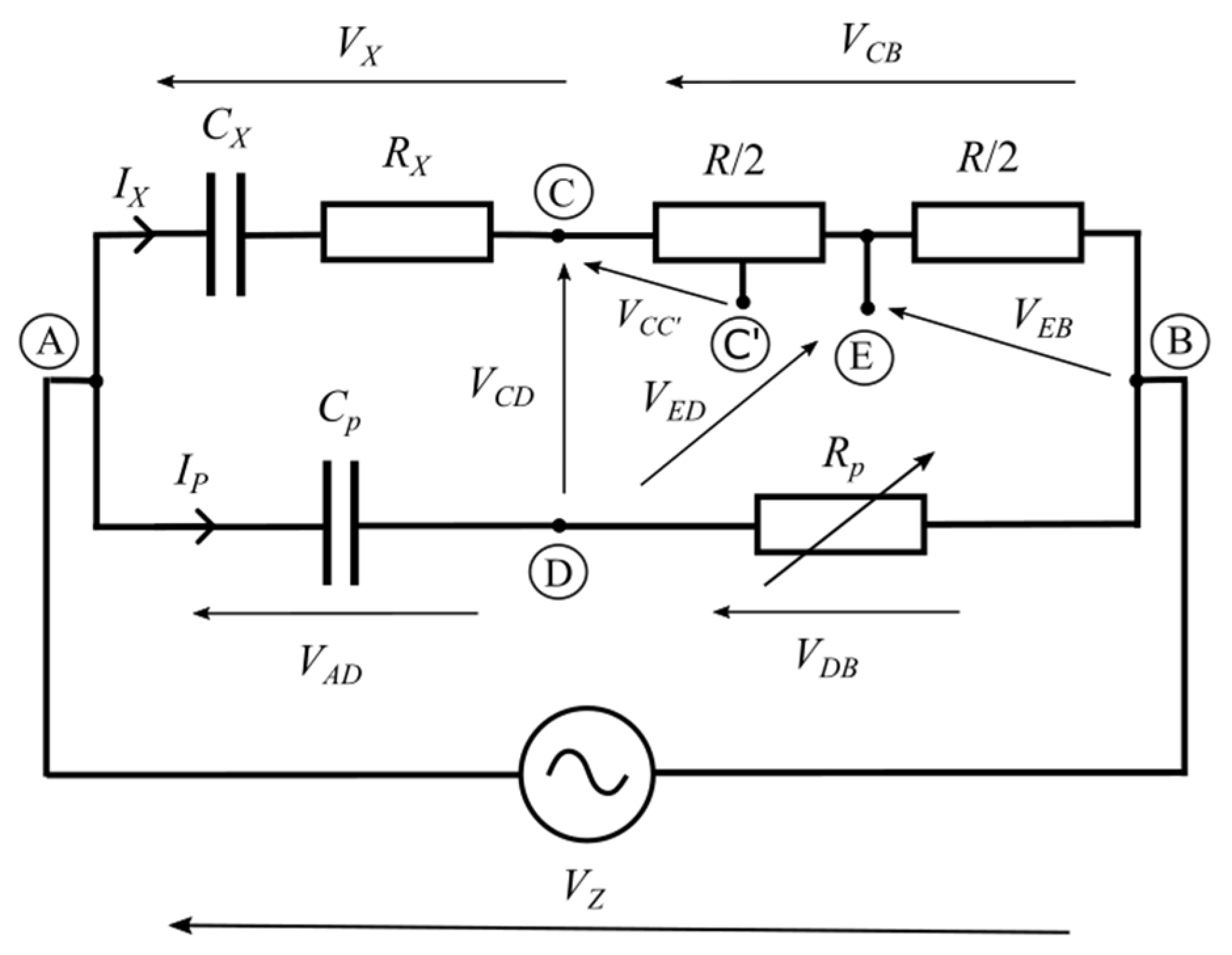
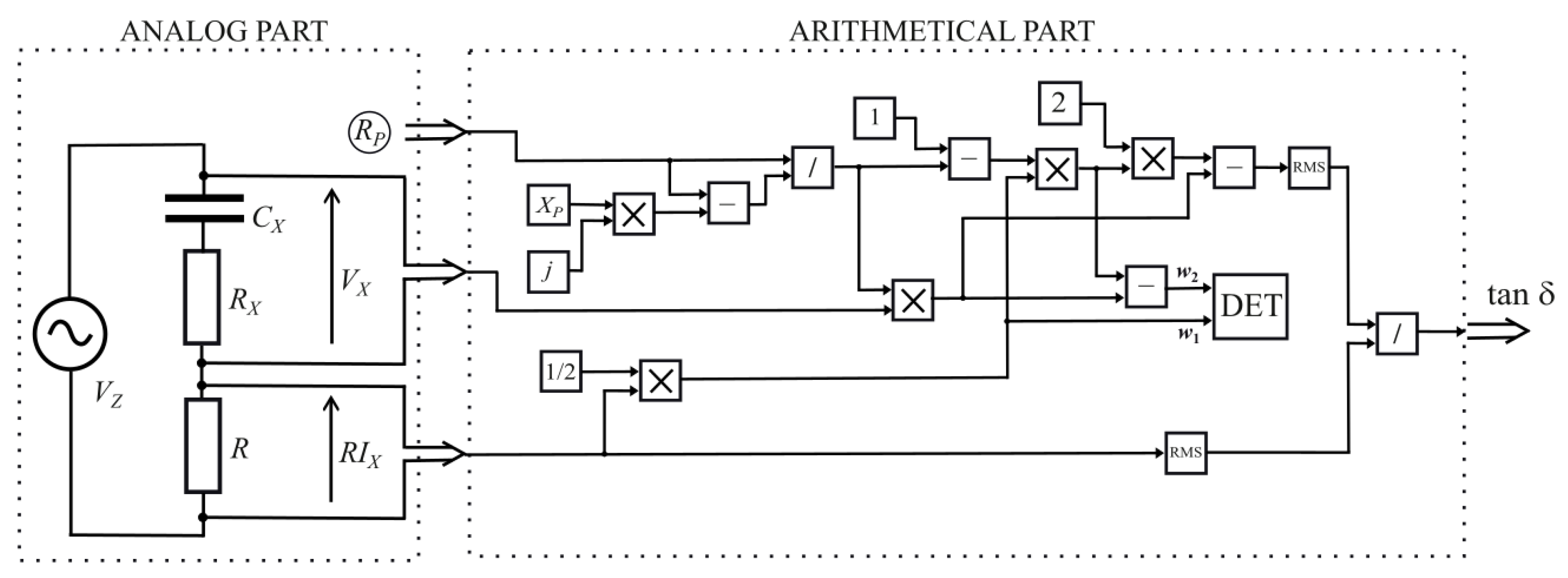
The synthesis of the non-bridge measuring system will be based on the principle of operation of the bridge system shown in
Figure 1. The bridge was first introduced over 60 years ago [
18]. At that time, even the analog implementation of such a system was problematic due to the properties of most voltmeters of the time. These were usually analog devices that were characterized by low input resistances. This, in turn, disrupted the flow of currents and the distribution of voltages in the bridge, making it practically impossible to implement.
The synthesized non-bridge measurement system will be a completely new one. The processing of measurement signals in impedance bridge is limited by the properties of RLC components forming the bridge. These components are characterized by limited values resulting from their design, the limited range of changes in these values, the resolution of settings, the presence of parasitic quantities (e.g., leakage of capacitors), limited power, and permissible voltages. In addition, conducted and induced interference occurs in such systems. Such problems do not exist in systems in which measurement signal processing is performed. Therefore, it is worth trying to build non-bridge systems that can be derived on the basis of known measurement systems by digitizing and virtualizing them. The processing in non-bridge systems is carried out by performing mathematical operations on signals. They are equivalent only to the voltage and current of the object being tested.
The bridge circuit is only the basis for deriving signal processing equations. The new non-bridge circuit can be implemented, for example, as a digital circuit with software signal processing.
The bridge, which is the basis of synthesis, is shown in
Figure 1. It is designed to measure the dielectric loss factor tan
δ. The concept of this bridge was presented in ref. [
12]. The principle of operation of the bridge is presented in an extremely concise way, making the analysis of the system somewhat difficult.
The transfiguration of the bridge from the original concept is presented in [
19].
The object of research in this study is a lossy capacitor, which has been modeled in a simplified way as a branch consisting of
CX capacitance and
RX resistance connected in series. For such a model, the dielectric loss factor can be expressed as follows:
The bridge has two adjustable elements: the RP resistor and the RCC′ resistor. The resistors in the CB branch have resistances equal to R/2, while the RCC′ resistor is part of the resistor switched on between the CE points and in practice can be implemented as a potentiometer, in which the C′ point is attached to the slider. The resistance of this resistor can take values from 0 to R/2. The system has two measurement steps, in which balancing of the system is performed twice.
The possibility of building the above system and the results of simulation studies of its basic properties are presented in ref. [
20]. This study confirmed the purposefulness of building such a system.
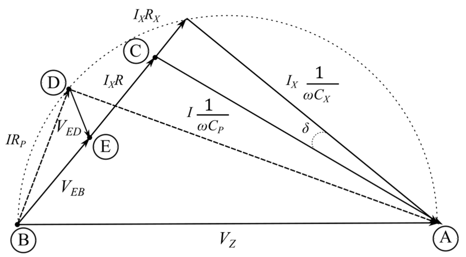
Figure 2 shows a phasor diagram of bridge voltages. When constructing the diagram, it was assumed that the supply voltage had a zero phase. The method of constructing graphs using the homographic function (Möbius transformation) presented in [
2] was used. Note that points A, B, C, and D are loci on the Gaussian plane of the potentials of the corresponding bridge points from
Figure 1.
The bridge requires two measurement steps. In the first measurement step, the RP resistor is the adjustable element. In this step, the VEB and VED voltage modules are compared. Such a comparison can be made, for example, by comparing the RMS values of the voltages. Note that in this balancing step, the current IX does not change during the measurement, which means that the VEB voltage remains unchanged throughout the measurement. The loci of points C and E do not change. Changing the RP resistor setting results in the D point moving along the ADB semicircle.
The measurement step completes the state in which the voltage preference lengths
VEB and
VED are equal to each other. This means that the
VED voltage module is equal to the
VEB voltage module:
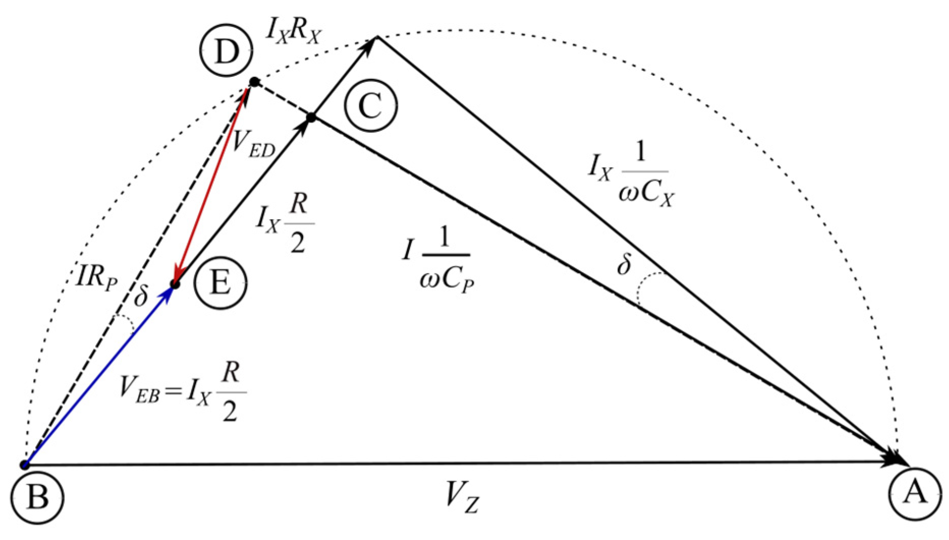
Figure 3 shows the phasor chart after the first balancing step is completed. On the diagram, it can be seen that due to the similarity of the triangles, the angle between the
VDB and
VBC voltages is equal to the angle δ of the object under control. You can also notice that the
VAC voltage is in phase with
VAD.
Analyzing the above diagram, it can be seen that it is possible to determine the sine of the angle δ as a voltage relationship between
VCD and V
CB. The author of ref. [
12] suggested another way to measure this relationship, as the resistance relationship between
RCC′ and
R. A second measurement step can be performed for this purpose. In this step, the adjustable element is the
RCC′ resistor. The value of the
RP resistance from the first step is maintained. The
VCD and
VCC′ voltage modules are compared. The bridge is brought to a state in which the voltage module
VCD is equal to the voltage module
VCC′:
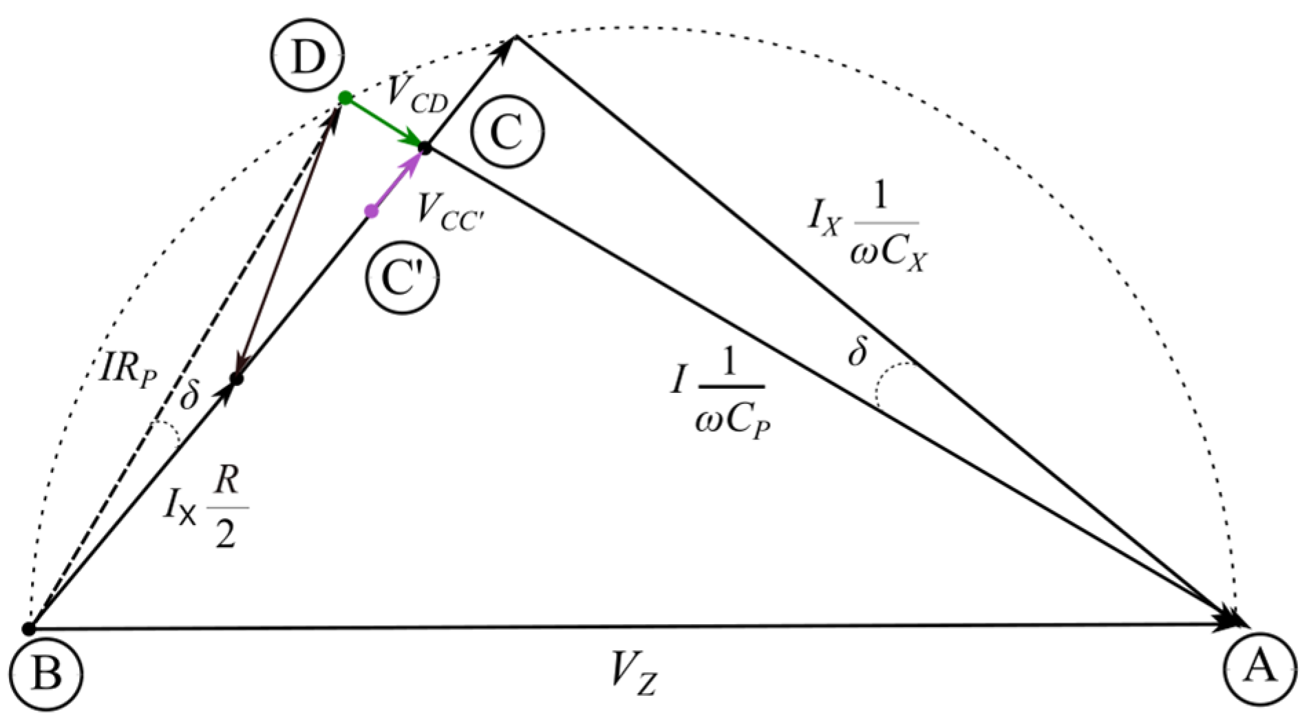
A phasor diagram after completing this step is shown in
Figure 4.
From the phasor diagram in this condition, it follows that the sine of the angle
δ can be calculated as follows:
From the sine, the tangent of the angle
δ can be calculated as follows:
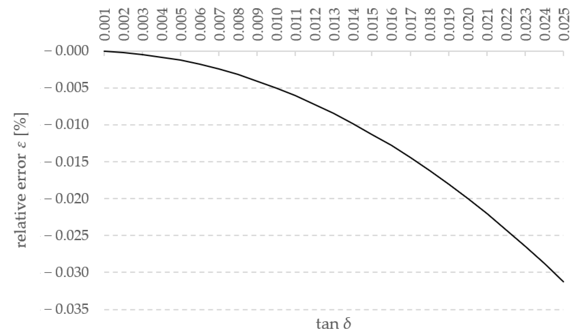
For low-loss capacitors, Equation (5) can be written in approximate form as follows:
The relative error
ε of the approximation (6) can be determined as follows:
Figure 5 shows the dependence of error (7) on the measured dielectric loss factor tan
δ.
From the assessment of the approximation error, it appears that for typical tan δ dielectric loss factors, the approximation error (6) is vanishingly small.
The analysis of the system shows that the second balancing step is actually used to determine the relationship (4). It allows you to determine the sine (or tangent) of the loss angle as a relation of two resistances. Perhaps the author of the concept intended this to facilitate the measurement by, for example, scaling the potentiometer in tan δ values. The measured dielectric loss factor can also be determined as a relationship between modules or values of effective voltages VCD and VCB, which can be easily implemented today. We should remember that voltage measurements in the period when the idea of the bridge was born were difficult due to the relatively low input resistance of devices and their low accuracy. The author states that voltmeter errors are eliminated because it is used only to determine the equality of voltages. However, it does not take into account the impact of module equality detection error on the measurement result.
3. Synthesis of a Non-Bridge System
In this bridge circuit, two signals from the impedance under study are processed: voltage
VX and current
IX. These signals require the application of the
VZ supply voltage. In the case of digital processing, the
IX signal should be converted to voltage, e.g., at a resistor, which acts as a shunt. Note that the supply voltage
VZ, together with the branch containing the impedance under test
ZX and resistor
R, is half of the bridge in
Figure 1. The other half can be realized in a different way, using transducers that allow the construction of a non-bridge system.
In the case of building a non-bridge equivalent to a bridge, the second measurement step can be omitted. In this case, the measurement will require only one measurement step. The bridge signals subject to detection are
VEB and
VED. In a non-bridge system, these will be the voltages marked as
w1 and
w2, described by the following equations:
The w1 signal can be realized by dividing the voltage drawn from resistor R by 2.
The
w2 signal can be written with a dependency:
where the impedance
ZP is equal to the following:
The relationship (9) can be rearranged to
By substituting the
VEB, determined by Equation (8), into Equation (11), it can be transformed into the form
After ordering Equation (12), the dependence on the output signal
w2 is obtained:
The
w2 signal can be obtained by multiplying the voltage and current signals by the appropriate coefficients. Notice that both coefficients contain the relation
RP to
ZP, which can be written as follows:
In relation (12), there is the setting parameter RP and the constant XP, which is the reactance of the capacitor CP. This relation is a complex number. In an analog measurement system, the multiplication by an imaginary unit j means a phase shift of 90°. This can be accomplished using a phase shifter. In digital realization, the multiplication by an imaginary unit can be accomplished by shifting the signal by the number of samples corresponding to 1/4 of the period.
After omitting the second measurement step, the measured dielectric loss factor can be determined from the voltage relation:
The corresponding voltages depending on (15) are equal to
and
The
VCD voltage can be written definitively as follows:
Figure 6 shows the structure of a non-bridge system for measuring the dielectric loss coefficient tan δ, derived from the equations describing the bridge in
Figure 1. The non-bridge system consists of two parts. The analog part contains the power source, the
ZX impedance under test, and the
R resistor of a known value. The output signals of the analog part are the voltage
VX across the impedance
ZX and the voltage proportional to its current
IX. The second part of the system is the arithmetic part, in which the detected voltages
w1 and
w2 are determined according to Equations (8) and (13), respectively. The modules or RMS values of the
w1 and
w2 signals are compared in the DET detector. In the equilibrium state, to which the system is driven by changing the
RP parameter, the measured tan
δ is determined by dividing the modules or the RMS values of the signals according to the relationship (13).
The arithmetic part of the circuit can be implemented in analog form. The problem in such a project is the need to build analog multiplication and division circuits as well as circuits determining the module or RMS value of the signals subject to detection.
In the case of digital implementation, the signals will be processed in analog–digital circuits and then processed by software. Operations that are difficult for analog signals are much simpler here.
4. Errors and Uncertainties
In the solution discussed, several sources of error and measurement uncertainty can be indicated. One source of uncertainty is the uncertainty of determining the measured dielectric loss factor from Equation (13). This coefficient is determined in the equilibrium state as a relationship of the values of the voltage modules
VCD and
VCB, but this relation can be determined as the ratio of the effective values of the voltages in question. Thus, the relative measurement uncertainty of the dielectric loss factor tan
δ, denoted as
urel (tan
δ), can be estimated as
where
urel(
VCD) and
urel(
VCB) are the uncertainty of determining the RMS value of the
VCD and
VCB voltages, respectively.
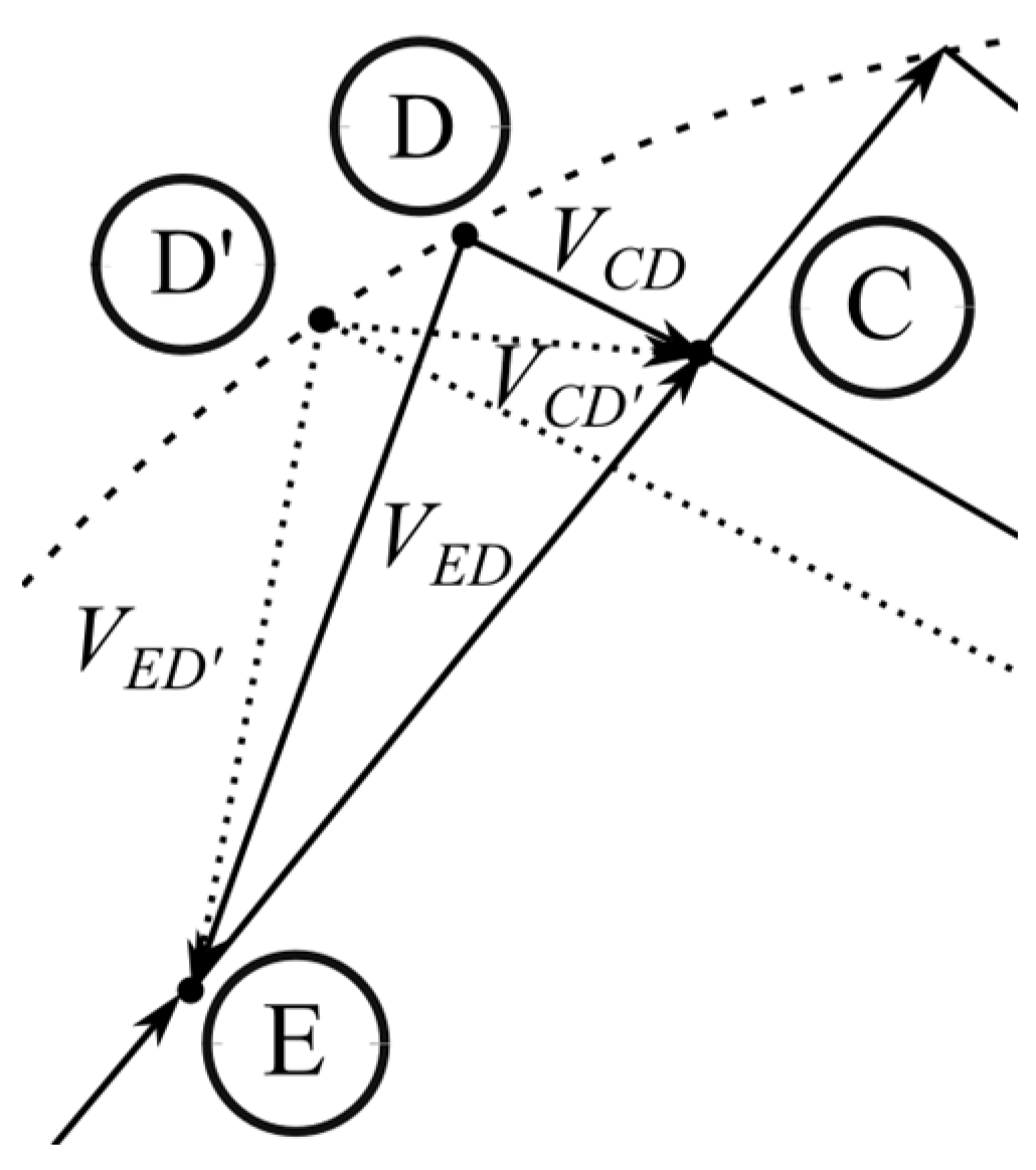
Other sources of error in the system in question are related to the incorrect position of the D point during measurement. This can be caused by an error in the detection of equilibrium and a loss of the
CP capacitor. In the first case, the equilibrium state of the bridge means the equality of modules and thus the values of the effective voltages
VEB and
VED. The inequality of the mentioned voltages, caused by the incorrect detection of their equality, results in the adoption of an equilibrium state despite the inequality of the
VEB and
VED voltage modules. Then, on the phasor diagram, the point D′ is taken as the potential of point D, which results in a change in the value of the voltage
VCD to the value of
VCD′.
Figure 7 shows an illustration of the loci of points D and D′ on the Gaussian plane. For readability, a fragment of the phasor chart is presented.
As a result of the incorrect position of the locus D, the dielectric loss coefficient tan δ determined from Equation (15) will have the value tan δ′ equal to the following:
The absolute error in determining the dielectric loss coefficient Δ tan
δD, caused by the shift in the point D, will have the following value:
The analytical calculation of this error is complicated. This is due to the need to calculate the modules of complex voltages. However, the error in determining the dielectric loss factor can be estimated by analyzing the phasor diagram shown in
Figure 7. On the diagram, it can be seen that the difference in voltage modules
VCD and
VCD′, for a small difference in voltage modules subject to detection
VED and
VED′, is approximately equal to this difference:
The error Equation (21) can then be written as follows:
The difference between VED and VED′ voltage modules, denoted as ∆VED, is an absolute error of modular detection.
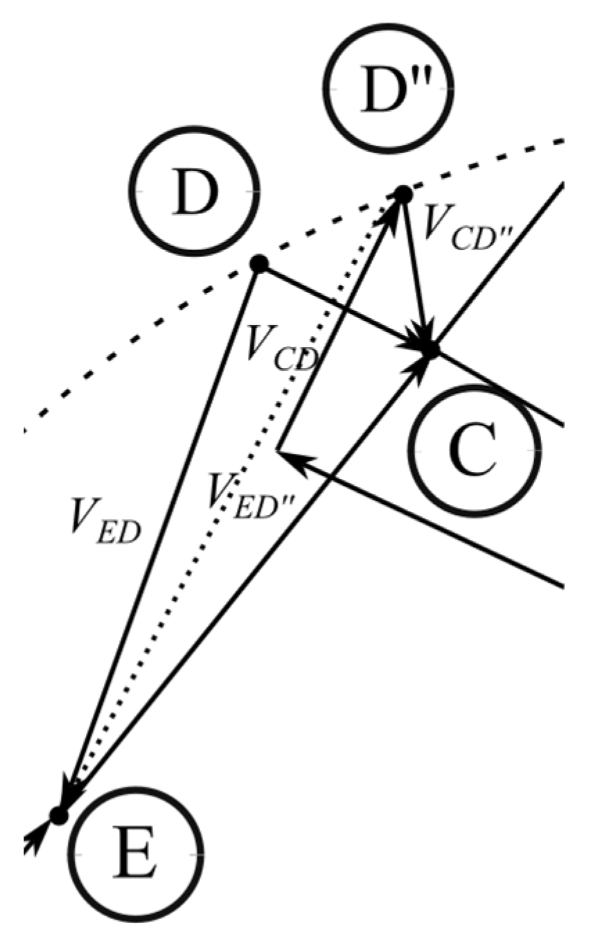
In the same way, the error related to the loss of the CP capacitor can be determined. In this case, the displacement of the D point will involve a change in the phase angle of the voltage across the lossy capacitor.
This offset can be estimated as the
VDD′ voltage from Equation (22). The error due to the loss of Δ tan
δL can then be estimated as
and thus
The vector of the voltage drop across the real component of the capacitor presented in
Figure 8 has been significantly scaled for the readability of the drawing. In fact, it is much smaller. The modulus of the voltage across the capacitor
CP can be approximated as equal to the voltage module
VDD’’. Then, the error caused by the capacitor′s loss factor can be estimated as
where tan
δCP is the loss factor of the capacitor
CP.
In a passive bridge circuit, the dielectric loss factor tan δCP should be much (several orders) lower than the measured dielectric loss factor tan δ. In a non-bridge circuit, the discussed error related to the quality of the CP capacitor does not occur. In these circuits, the source of analogous error will be the realization of multiplication by the imaginary unit j. In the analog circuit, the source of this error will be the inappropriate phase shift in the shifting switch, different from 90°. On the other hand, in a system that performs digital signal processing, the source will be the realization of the shift in the vector of measurement signal samples by a time corresponding to 1/4 of the waveform period.
5. Discussion and Conclusions
This evaluation allowed us to develop the concept of a non-bridge measurement system designed to measure the dielectric loss coefficient of a real lossy capacitor modeled as a series connection of RC elements.
For the purpose of synthesis of a non-bridge system, it is necessary to derive equations describing the signals to be detected. In a bridge system, the measurement process requires bringing two selected bridge voltages to a state in which their modules are equal. This state also means equality of the effective values of these tensions. In ref. [
18], the derivation of the equation for the measured tan δ was based on the geometric analysis of the phasor diagram. When signals are subject to detection using the symbolic method, in which they are complex numbers, it can be seen that the determination of modules or effective values is very complex, and thus the determination of the processing equation is also complex.
Using the derived equations for the signals subject to detection, the structure of a non-bridge system was developed. It was also noted that the method proposed by the author of the bridge required two balancing steps. In the second step, the purpose of balancing was to determine the voltage relation, which could be determined as a resistance relation. However, it turned out that this method unnecessarily complicates the measurement process. It would also require the use of an adjustable resistor, the design of which would be very troublesome. It seems much easier to determine the measured coefficient from the voltage relations of the circuit. The presented structure of a non-bridge circuit requires taking the voltage of the tested lossy capacitor and the voltage proportional to the current of this capacitor. This voltage can be taken from the appropriate shunt. As you can see, the design of the analog part is very simple and consists only of a supply voltage generator and a shunt. Further signal processing can be performed by analog or digital measurement. The digital implementation is simpler and allows the trouble-free setting of parameter values corresponding to the values of bridge elements. The operations carried out on the signals in the processing chain are also very simple. Only the operations of shifting by 1/4 of the period corresponding to multiplication by the imaginary unit and the operation of determining the modulus or RMS values can be slightly more complex, which can be simplified into the procedure of finding the maximum in a set of samples taken for the period.
Errors and uncertainties of the system were also assessed. Here, too, the analytical determination of the value of errors and uncertainty poses considerable difficulties. However, it is possible to make an approximate estimate, indicating the possibility of using the proposed system in practice, e.g., measuring tan δ in the assessment of the degradation of insulation materials.
A significant advantage of this system is the constant maximum convergence. The balance process is much simpler than in typical bridge systems. Only one control element is used to reach equilibrium, which in a non-bridged system means a change in the value of only one parameter. Other advantages of the non-bridge system are the possibility of setting wide values for the regulated parameter, no interference affecting the RC elements of the bridge, and no influence from the parasitic parameters of the reference capacitor on the measurement.
Further work on the method should focus on comparing different implementations of the described system and on a broad examination of the selected project, e.g., its application to testing insulating materials.


