Abstract
HTS 2G tapes used in Superconducting Fault Current Limiters (SFCLs) have properties that allow for the effective limitation of short-circuit currents; however, due to the specificity of the device operation, they should be characterized by the high stability of the parameters when repeatedly leaving the superconducting state. During the operation of SFCLs, a situation may occur in which the parameters of the HTS tapes used will change several times as a result of the action of short-circuit currents that exceed the critical current IC of the superconductor of the tape used. This paper presents the results of microstructural tests of 2G HTS tapes intended for SFCLs, subjected to surge currents corresponding to prospective short-circuit currents with values higher than their critical currents IC and for which IC changes were observed. The HTS tapes were examined using a JEOL 7600F field emission scanning electron microscope (SEM), and their chemical composition was analyzed using Energy-Dispersive X-ray Spectroscopy (EDS). The test results indicate the possibility of micro-damage in the form of cracks in the superconductor layer, as well as the interruption of the buffer layers and the oxidation of the silver layers. The analysis of the chemical composition of the HTS tape layers may indicate the occurrence of diffusion processes.
1. Introduction
Superconducting Fault Current Limiters (SFCLs) are devices designed to limit short-circuit currents, most often based on high-temperature superconductors. They use the physical properties of a superconductor, which transition from a superconducting state to a resistive state as a result of exceeding one of the critical parameters. The SFCL is characterized by a fast operation, which is related to the very short transition time of the superconductor from the superconducting state to the resistive state [1,2,3,4,5,6,7]. In the resistive state, the SFCL can effectively limit short-circuit currents [1,2,3,8,9,10].
The superconducting element of the SFCL is constructed from high-temperature superconducting tapes made using thin-film technology [11]. Buffer layers and a superconductor are applied to the Hastelloy stainless steel substrate. The HTS tape is covered with silver layers on both sides, and can additionally be covered with a copper stabilizer layer. Hastelloy constitutes over 94% of the HTS tape components and is made of a non-magnetic alloy with a high resistivity with the following composition: 57% Ni, 15% Mo, 15.5% Cr, 5.5% Fe, 4% W, and 2.5% Co [12]. Hastelloy is characterized by good mechanical properties that improve both the elasticity of the superconductor and its thermal stabilization. Buffer layers increase the adhesion of the superconductor to the Hastelloy substrate and also constitute a diffusion barrier [13].
The 1 μm thick superconductor layer is made of YBCO (sometimes rare earth elements, ((RE)BCO), are used instead of yttrium). As ceramic materials, YBCO contains certain imperfections in its structure in the form of grains separated by boundaries and scarring. This affects the transmission of currents with a high critical density [14].
It is known from literature studies that mechanical damage (deformation) may occur in HTS tapes as a result of currents higher than critical currents [15,16], the separation of the stabilizer layer [17,18], damage at the soldering points [16,19], as well as changes in the critical current value [16,18,20,21,22,23]. In [23], it was suggested that the cause of the degradation of the critical current value may be perforations in the superconducting layer. The research results described in [15,16,17,18,19,20,21,22,23] indicate that macroscopic changes in the tapes were responsible for the IC degradation. In [24], the influence of prospective short-circuit currents on the change in the HTS tape parameters was studied. They confirmed that changes in the IC values can occur despite the lack of macroscopic changes in the tapes. Multiple SFCL activations may cause micro-damages in the superconductor layer, which are responsible for changing the critical current of the tape. The main objective of this paper is to determine the causes of the changes in the critical current value due to the action of surge currents based on comparative microstructural studies of new (unused) samples and samples with reduced IC values using a JEOL 7600F field emission scanning electron microscope (SEM).
2. Tested Materials
The 2G HTS tapes with a YBCO superconductor, with a critical temperature of about 92 K [25], were made in the form of layered tapes with a composite structure with a coated conductor, made using multilayer technology. The construction of the 2G HTS tapes from SuperPower is shown in Figure 1 [26]. The parameters of the tested HTS tapes intended for the SFCL construction are presented in Table 1 and Table 2.
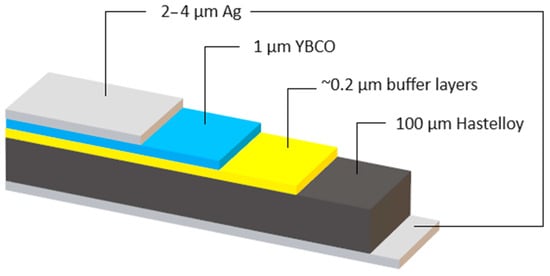
Figure 1.
Construction of the 2nd generation HTS YBCO tape by SuperPower.

Table 1.
Buffer layer structure in the 2G HTS tapes.
Table 2.
Parameters of the 2G HTS tapes without the copper stabilizer by SuperPower.
Figure 2 shows the R(T) characteristics obtained from the measurements for the 2G HTS tapes from SuperPower made for a 10 cm long sample. After cooling to 77 K (using a liquid nitrogen bath), the HTS tapes were placed in air at room temperature and heated to 320 K with warm air; then, the change in the resistance as a function of the temperature was examined. The HTS tapes selected for the testing had different resistance–temperature characteristics due to the different thicknesses of the silver layer. As a result of the surge currents of the HTS tapes, they can heat up to different temperatures, different amounts of energy will be released on the tested samples, and they will also limit the prospective short-circuit currents with different levels of effectiveness.
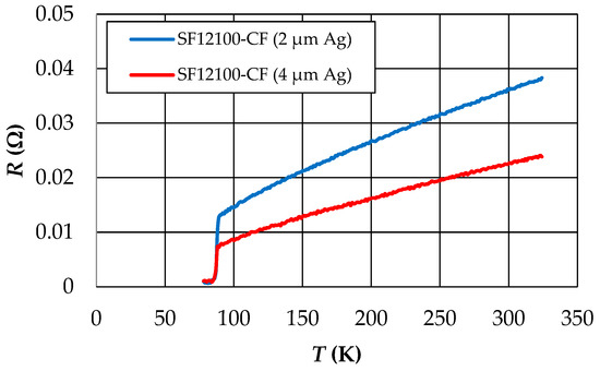
Figure 2.
R(T) characteristics of the 2G HTS SF 12100-CF tapes.
3. 2G HTS Tape Sample Preparation Station
To prepare the 2G HTS tapes, a stand was built, as shown in Figure 3, consisting of current transformers that allowed for the obtainment of an output current of up to 1 kA (in a short circuit) at a voltage of 6 V (in an idle state), a digital oscilloscope, a cryostat with liquid nitrogen, and a programmable voltage source IT7626 with a power of 3 kVA. The current flowing through the HTS tapes was measured with a current probe with a range of 1 kA and the voltage was measured with a 1:1 voltage probe [27,28]. The proposed system enabled the testing of samples in conditions similar to the actual operating conditions of the superconducting tape in the SFCL installed in the MV network.
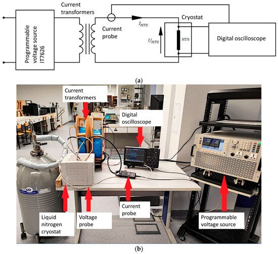
Figure 3.
Measurement system: (a) diagram of the measurement system; (b) view of the measurement station.
The method of attaching the HTS tape samples in the measuring holder is shown in Figure 4. The lengths of the tested samples were 10 cm. The HTS tape samples were attached to the measuring holders with copper current terminals. The contact area of the tape with the terminals was 240 mm2, which ensured a voltage drop at the Cu-Ag interface, which can be estimated at about 0.5% of the measured voltages [27,28].
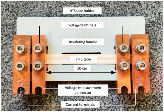
Figure 4.
Method of attaching the HTS tapes to the measuring holder.
4. Preparation of HTS Tape Samples
4.1. Method of Measuring the Critical Current Value
The critical current values of the HTS tapes provided by the manufacturers were determined with direct current excitation [29]. However, the operation of SFCLs in sinusoidal alternating voltage systems requires the determination of the critical current value for this type of supply. Therefore, a method was developed to determine the IC with this type of supply. The method of determining the critical current with sinusoidal excitation at a frequency of 50 Hz is shown in Figure 5. The critical current of the HTS tape was determined with a test current I at a frequency of 50 Hz and a duration of 100 ms, and the critical current of the tested samples was assumed to be the minimum value of the test current amplitude that initiated the sample’s transit from the superconducting state. The value of the critical current IC was determined by gradually increasing the amplitude of the current I in the tested sample. The transition of the tape to the resistive state was identified as an increase in the voltage on the sample and a decrease in the current value, which was caused by an increase in the temperature and the resistance of the tape. For test currents I smaller than the critical current IC, the amplitude of the superconducting current had a constant value, and the voltage on the sample had a small value related to the junction resistance (Figure 5a). After leaving the superconducting state, the voltage on the sample increased and the current value was limited (Figure 5b).
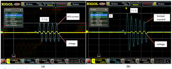
Figure 5.
Current and voltage waveforms for the HTS tape: (a) the sample in the superconducting state; (b) the sample in the resistive state.
4.2. Test Current Impulse
Figure 6 shows an example of a test current impulse waveform illustrating the principle of short-circuit limitation by a superconducting short-circuit current limiter. As a result of the increase in temperature and the resistance of the HTS tape, the voltage on the sample gradually increased and the current value decreased. The prospective short-circuit current (Ipsc) is the current that would flow in the considered circuit if it were not limited as a result of the HTS tape transition the superconducting state. The prospective short-circuit current impulse is called the test current. The test current, after reaching a value equal to the critical current IC, caused the HTS tape to transition the superconducting state. The maximum instantaneous value of the prospective short-circuit current was called the surge current (Imax). The current that flowed in the circuit in the resistive state was called the limited short-circuit current [24].
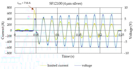
Figure 6.
Sample oscillogram of the test current pulse waveform for the SF12100-CF tape with a 4 µm silver layer illustrating the principle of short-circuit limitation by the SFCL.
4.3. Determination of the Energy Generated on the HTS Tape
For the tested tape, the value of the energy released in a single sample was determined for the applied test current impulse based on the recording of n discrete current and voltage values on the oscilloscope. The formula used to calculate the energy value is defined as follows [28]:
where E—the amount of energy generated on the sample, Δt—the impulse duration, uk—the discrete value of the voltage on the tape, ik—the discrete value of the current, k—the measurement number, and n—the number of measurements of the discrete current and voltage values.
4.4. HTS Tape Sample Parameters
For the microstructural tests, HTS tape samples were prepared which, as a result of the multiple transitions from the superconducting state with a test current impulse, showed a decrease in the critical current value (Table 3). Tests of the SF12100-CF tapes with 4 µm and 2 µm thick silver layers were performed for one value of the prospective short-circuit current. The critical current IC was measured for the unused HTS tapes, and then the samples were subjected to 25 series of test current impulses with a duration of 0.2 s, and the IC value was measured again. The duration of the test current impulse was selected in such a way that it corresponded to the typical operating times of the short-circuit protection of the MV power system protection. The values of the surge current Imax, the released energy E during the impulse, and the voltage drop Udrop on the sample are presented in Table 3. In order to determine the possible causes of the changes in the critical current value, comparative microstructural studies were conducted using a scanning electron microscope for the samples subjected to surge currents and control (unused) samples.
Table 3.
Critical current values of the SF12100-CF tape samples used for the microstructural tests.
5. HTS Tapes Studies Using Scanning Electron Microscope
5.1. Research Methodology
In order to observe the changes in the internal structure, the HTS tapes were examined using a field emission scanning electron microscope (FE-SEM). The chemical composition was analyzed using the INCA OXFORD Energy-Dispersive X-ray Spectroscopy (EDS). The measurement stand is shown in Figure 7. The following measurement conditions were used during the tests:
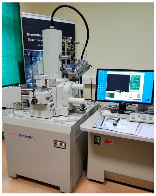
Figure 7.
Measuring station with the scanning electron microscope.
- A scanning probe current intensity of 8 mA;
- An electron beam acceleration voltage of 7–8 kV.
Figure 8 shows the HTS tape samples embedded in conductive resin.
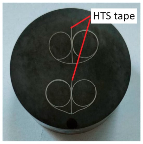
Figure 8.
Samples of cross-sections of HTS tapes embedded in conductive resin.
5.2. Scope of Research
Figure 9 shows photos of the cross-sections of the HTS tapes: Figure 9a—the control sample; Figure 9b—the sample exposed to prospective short-circuit currents, for which the critical current value decreased.
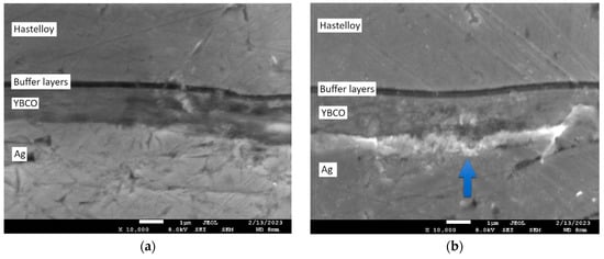
Figure 9.
Cross-sectional photos of the HTS tapes taken using an electron microscope: (a) control sample; (b) sample exposed to prospective short-circuit currents.
In the sample subjected to the expected short-circuit currents, changes (marked with a blue arrow) are observed at the silver–superconductor boundary, indicating the possibility of certain changes between these layers. In order to identify these changes, an analysis of the microstructural changes and chemical compositions for individual layers in the HTS tapes was carried out. The tests were carried out for the following four cases: the SF12100-CF tape with silver layers of 4 μm and 2 μm thicknesses, control samples (new), and samples for which a decrease in the critical current IC value was recorded as a result of the expected short-circuit currents. The thicknesses of the silver, superconductor, buffer layers, and Hastelloy substrate layers of the HTS tapes were measured using the PCSem program, and the spectra were downloaded for each layer to identify their chemical compositions.
5.3. Measuring the Thickness of HTS Tape Layers
Figure 10 shows sample photos of the SF12100-CF tape control sample with a 4 μm silver layer, with the thicknesses of the individual HTS tape layers marked. Analogous measurements were made for the remaining samples. Table 4 presents the results of the layer thickness measurements for the four samples of the tested HTS tapes.
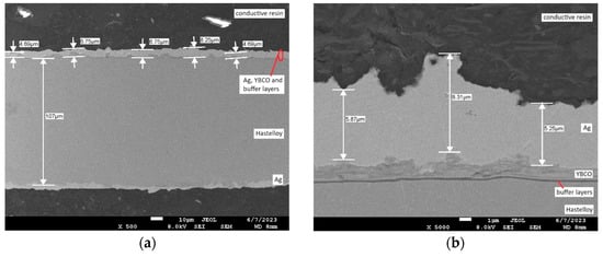
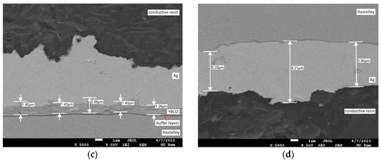
Figure 10.
Sample photos of the HTS tape cross-section (4 µm Ag)—control sample: (a) the entire width of the cross-sectional area, (b) the upper Ag layer, (c) the YBCO layer, and (d) the lower Ag layer.
Table 4.
Average layer thicknesses in the HTS tapes.
Based on the measurements, it can be concluded that the thicknesses of the HTS tape layers differ from those given in the product specifications. In the control samples, the silver layers had different dimensions than in the samples subjected to the prospective short-circuit currents—both for the top and bottom layers. The superconductor layers also had different thicknesses. In the control samples, they were almost half as thick. In addition, a large inhomogeneity was observed in the thicknesses of all the layers in the samples.
5.4. Changes to HTS Tape Images
Based on the analysis of the microscopic images, characteristic changes in the appearance of the HTS tapes can be seen for the samples subjected to prospective short-circuit currents. Figure 11 shows photos of the SF12100-CF tape with a 4 μm silver layer—Figure 11a shows a cross-section of the control sample and Figure 11b shows a sample subjected to prospective short-circuit currents. The differences concern changes at the silver–superconductor boundary. In the control sample, the boundary between the layers is clearer, and the shades of both layers are uniform. In the second sample, the proportions of the layer thicknesses have changed, and cracks in the superconductor layer are visible (vertical arrows) and have clearly lighter areas (horizontal arrow).
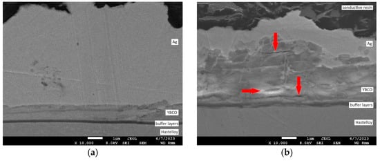
Figure 11.
Photos of the SF12100-CF tape with a 4 μm silver layer: (a) cross-section photo of the control sample; (b) cross-section photo of the sample exposed to the prospective short-circuit currents with marked changes in the YBCO layer.
Similar changes were observed for the SF12100-CF tape with a 2 μm silver layer. Figure 12 shows a photo of the sample subjected to the prospective short-circuit currents, and shows cracks in the superconductor layers and brighter areas, marked with red arrows, as well as discontinuities (cavities) in the buffer layers, marked with green arrows. The identification of the changes required an analysis of the chemical composition of the HTS tape layers.
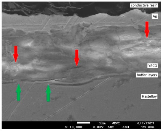
Figure 12.
Changes in the sample of the HTS tapes SF12100-CF (2 μm Ag) exposed to prospective short-circuit currents.
5.5. Chemical Composition Analysis of the SF12100-CF Tape (4 μm Ag)—the Control Sample
For the tested sample, the chemical composition of the individual layers of the tape was analyzed. Figure 13 shows the SEM images of the HTS tape cross-section with the area marked for which the analysis was performed (pink rectangle), as well as the obtained EDS spectra and chemical composition—the result was normalized to 100% by mass and atom.
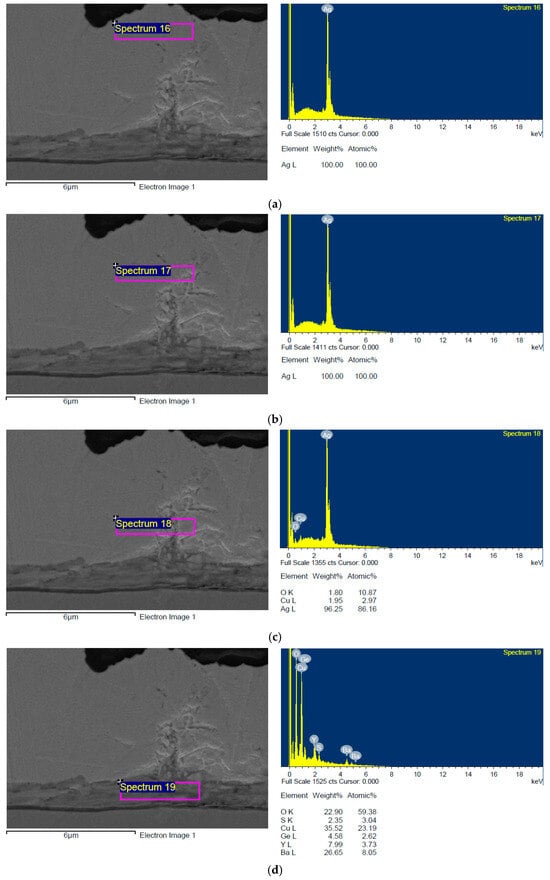
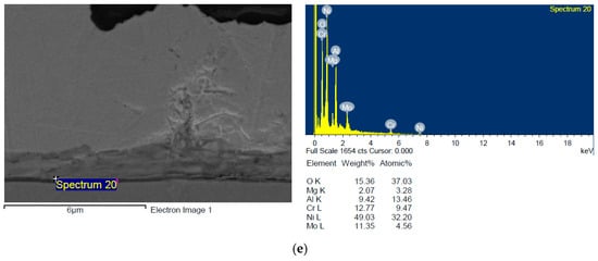
Figure 13.
SEM images of the cross-section of the HTS tape (4 μm Ag)—the control sample—and EDS spectra for the evaluation of the elemental composition: (a–c) the area corresponding to the silver layer, (d) the superconductor layer, and (e) the buffer layers.
The top layer of the HTS tape, including the silver, the YBCO superconductor, and buffer layers, was subjected to a detailed evaluation of the chemical composition. Figure 13a–c show the areas of the measurement of the silver layer at three levels due to the large thickness of the Ag layer in this place of the sample and the deformation visible in the photo. Spectrum 16 is located closest to the outer surface of the HTS tape (near the non-conductive resin). Spectrum 17 is located in the middle part of the layer, while Spectrum 18 is located closer to the Ag-YBCO boundary and covers part of the area with the deformation. For Spectrum 18, the presence of copper and oxygen (characteristic of the YBCO layer) was observed, which may indicate that the visible deformation probably occurred at the stage of the HTS tape production. The next areas examined (Spectrum 19) are the YBCO superconductor and the buffer layers (Spectrum 20). The chemical composition of the individual layers is consistent with the manufacturer’s description [12].
5.6. Analysis of the Chemical Composition of the SF12100-CF Tape (4 μm Ag)—the Sample with Reduced Critical Current Value
Figure 14 shows the SEM images of a cross-section of the SF12100-CF tape (4 μm Ag) exposed to prospective short-circuit currents and a reduced critical current value, with the area for which the analysis was performed (pink rectangle), and the obtained EDS spectra and chemical composition marked.
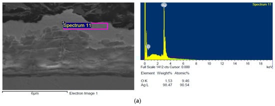
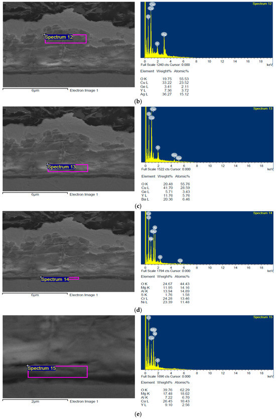
Figure 14.
SEM images of the HTS tape cross-section (4 μm Ag) and EDS spectra for the elemental composition assessment—the sample with reduced critical current value: (a) the area corresponding to the silver layer, (b) the area of the elements from the silver and superconductor layers, (c) the superconductor layer, and (d,e) the buffer layers.
The results of the chemical composition analysis showed changes in the area of the presence of the silver and the superconductor. In the area (Spectrum 11) with a thickness of about 2 μm, the presence of silver and small amounts of oxygen (1.53%) are mainly recorded. The cause of the presence of oxygen may be the oxidation process of the upper silver layer. In the area (Spectrum 12) apart from the silver, there is a significant amount of copper and oxygen, as well as small amounts of yttrium and germanium. The presence of these elements is typical for the superconductor layer, which was lower in the control sample. This may indicate the occurrence of certain diffusion processes between these layers. In the next area (Spectrum 13), only elements originating from the superconductor are present and no presence of silver is observed. In the remaining examined areas (Spectrum 14 and Spectrum 15), there are mainly elements characteristic of buffer layers and the Hastelloy substrate.
5.7. Analysis of the Chemical Composition of the SF12100-CF Tape (2 μm Ag)—the Control Sample
Figure 15 shows the SEM images of a cross-section of the SF12100-CF tape (2 μm Ag)—the control sample—with the area marked for which the analysis was performed (pink rectangle), and the obtained EDS spectra and chemical composition.
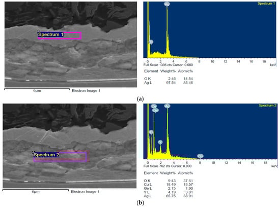
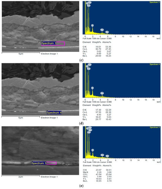
Figure 15.
SEM images of the cross-section of the HTS tape (2 μm Ag)—the control sample—and the EDS spectra and elemental composition evaluations: (a) the area corresponding to the silver layer, (b,c) the superconductor layer, and (d,e) the buffer layers.
The chemical composition analysis in the area—Spectrum 1—with a thickness of about 2 μm, mainly with the presence of silver and small amounts of oxygen (2.46%), is recorded. In the area—Spectrum 2—there are significant amounts of silver (65.75%), but, at the same time, the presence of copper (18.49%) and oxygen (9.43%), as well as small amounts of germanium and yttrium, are found. The measurement was performed at a level of about 2–2.5 μm, i.e., in the area of the silver–YBCO boundary (which is difficult to identify in the photo), which may be the reason for the occurrence of elements in both layers. In the next area—Spectrum 3—there are only elements originating from the superconductor. In the remaining examined areas (Spectrum 4 and Spectrum 5), there are mainly elements characteristic of buffer layers.
5.8. Chemical Composition Analysis of the SF12100-CF Tape (2 μm Ag)—the Sample with Reduced Critical Current Value
Figure 16 shows the SEM images of a cross-section of the SF12100-CF tape (2 μm Ag)—a sample with a reduced IC value—with the area for which the analysis was performed marked (pink rectangle), and the obtained EDS spectra and chemical composition.
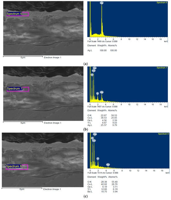
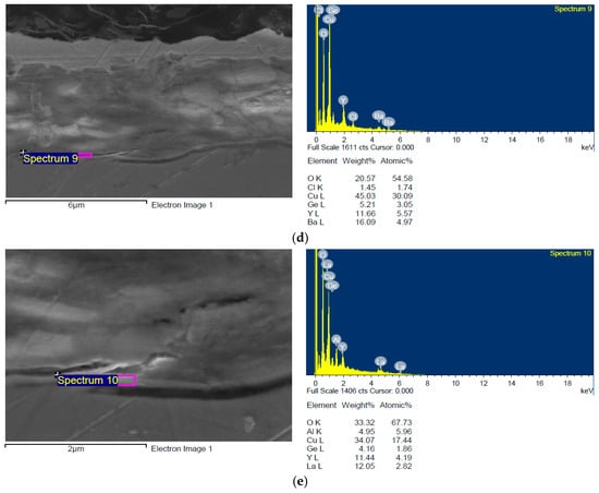
Figure 16.
SEM images of the HTS tape cross-section (2 μm Ag) and EDS spectra for the elemental composition assessment—the sample with reduced critical current value: (a) the area corresponding to the silver layer, (b) the area of elements from the silver and superconductor layers, (c) the superconductor layer, and (d,e) the buffer layers.
The analysis of the elemental composition in the first area (Spectrum 6) showed only silver (Figure 16a). Then, at the level of about 2–2.5 μm (Spectrum 7), similarly to the control sample, silver, copper, germanium, and yttrium were present, but the silver content dropped from 65.75% to 25.53%, while the amount of oxygen (from 9.43% to 22.67%) and copper (from 18.49% to 38.53%) increased significantly. The content of other elements characteristic of the superconductor also increased. Similar to the tape with a 4 μm thick silver layer with a reduced IC value, this may indicate the occurrence of diffusion between the silver and YBCO. In this area, there were also bright areas that may indicate silver oxidation. In the area—Spectrum 8—only elements originating from the superconductor occur. In the lowest areas (Spectrum 9 and Spectrum 10), there are elements characteristic of the buffer layers, but also elements from the YBCO layer.
In the tested samples (the control sample and the samples subjected to the expected short-circuit currents), no significant changes in the amount of copper and oxygen for the YBCO layer are observed. It is difficult to provide an unambiguous interpretation of the individual results obtained. More complete information could be obtained based on the study of a large number of samples and statistical analyses of the obtained results.
6. Discussion
As a result of the measurements, it can be stated that the parameters of the HTS tapes, regarding the thickness of their component layers, differ from those provided by the manufacturer. At the same time, there is a large inhomogeneity in the thicknesses of these layers for all samples, which was shown in the microscopic images. Thicker silver layers were found for the tape with a declared thickness of 4 μm (this tape had a lower resistance after leaving the superconducting state). Despite the lack of macroscopic changes for the tested HTS tape samples, it was possible to identify microscopic changes that could indicate the occurrence of diffusion processes responsible for changes in the IC values of the HTS tapes. In the photos of the samples subjected to surge currents (higher than IC), expanded layers are visible, which were initially identified as the superconductor layers. However, the analysis of their chemical composition showed the presence of elements from both the Ag and YBCO layers (especially for the areas closer to the Ag-YBCO boundary).
The top layer of the HTS tapes, including the silver and superconductor layers and the buffer layers, was subjected to detailed analysis. The evaluation of the chemical composition of the individual layers allows for the indication of their position in the sample. In the samples with a reduced critical current value, there were lighter areas for which an increased presence of oxygen (approximately 20%) was observed in the chemical composition—the presence of oxygen is characteristic of the superconductor layer. The presence of lighter areas may correspond to the presence of silver oxides. On the other hand, the analysis of the chemical composition of the superconductor layers of these samples indicates the occurrence of damage to the YBCO layer (changes in thickness and the presence of silver), which may be caused by diffusion processes, and which may consequently lead to a decrease in the critical current value.
The tested samples showed defects in the form of deformations and cavities in the buffer layers, and cracks at the silver–YBCO interface and in the superconductor as a result of the action of surge currents on the tape.
7. Conclusions
- HTS tapes subjected to surge currents show defects in the form of deformations and cavities in the buffer layers, and cracks at the silver–YBCO interface and in the superconductor.
- As a result of the exposure of the HTS tapes to surge currents, diffusion processes may occur between the silver and YBCO layers, and the silver layer may oxidize.
- Changes in the superconducting layer may result in a reduction in the critical current value of the HTS tapes.
- In order to determine the quantitative diffusion changes in the individual layers of superconducting tapes subjected to the expected surge current Ic, it is necessary to perform tests on a large number of samples and to perform statistical analyses of the obtained results.
Author Contributions
Conceptualization, S.H. and A.K.; methodology, S.H., A.K., P.S., K.A. and M.M.; validation, S.H., A.K., P.S., K.A. and M.M.; formal analysis, S.H., A.K. and P.S.; investigation, S.H. and K.A.; data curation, S.H. and A.K.; writing—original draft preparation, S.H. and P.S.; writing—review and editing, P.S.; supervision, S.H. and A.K. All authors have read and agreed to the published version of the manuscript.
Funding
This work was partially supported by a program of the Polish Ministry of Science under the title ‘Regional Excellence Initiative’, project no. RID/SP/0050/2024/1.
Institutional Review Board Statement
Not applicable.
Informed Consent Statement
Not applicable.
Data Availability Statement
The data presented in this study are available on request from the corresponding author due to privacy.
Conflicts of Interest
The authors declare no conflicts of interest.
References
- Yadav, S.; Bharati, K.; Tewari, V. Superconducting Fault Current Limiter—A Review. Int. J. Appl. Eng. Res. 2019, 14, 1–6. [Google Scholar]
- Rao, V.V.; Kar, S. Superconducting Fault Current Limiters—A Review. Indian J. Cryog. 2011, 36, 14. [Google Scholar]
- Nagarathna, M.C.; Murthy, H.V.; Shashikumar, R. A Review on Super Conducting Fault Curremt Limiter (SFCL) in Power System. Int. J. Eng. Res. Gen. Sci. 2015, 3, 485–489. [Google Scholar]
- Kar, S.; Rao, V. Step-by-step design of a single phase 3.3 kV/200 A resistive type superconducting fault current limiter (R-SFCL) and cryostat. Phys. C Supercond. Its Appl. 2018, 550, 107–116. [Google Scholar] [CrossRef]
- Zhang, Y.; Dougal, R.A. State of the Art of Fault Current Limiters and their Applications in Smart Grid. In Proceedings of the 2012 IEEE Power and Energy Society General Meeting, San Diego, CA, USA, 22–26 July 2012; pp. 1–6. [Google Scholar] [CrossRef]
- Ko, S.-C.; Han, T.-H.; Lim, S.-H. Power consumption and cumulative energy of bridge type SFCL with simultaneous quench. Phys. C Supercond. Its Appl. 2022, 592, 1354001. [Google Scholar] [CrossRef]
- Lee, H.-Y.; Asif, M.; Park, K.-H.; Lee, B.-W. Assessment of appropriate SFCL type considering DC fault interruption in full bridge modular multilevel converter HVDC system. Phys. C Supercond. Its Appl. 2019, 563, 1–6. [Google Scholar] [CrossRef]
- Alam, M.S.; Abido, M.A.Y.; El-Amin, I. Fault Current Limiters in Power Systems: A Comprehensive Review. Energies 2018, 11, 1025. [Google Scholar] [CrossRef]
- Ganev, G.; Hinov, K.; Karadzhov, N.; Kostov, D. Solid-state switches for fault current limiter control. In Proceedings of the 2014 18th International Symposium on Electrical Apparatus and Technologies (SIELA), Bourgas, Bulgaria, 29–31 May 2014; pp. 1–4. [Google Scholar] [CrossRef]
- Jo, H.-C.; Joo, S.-K.; Lee, K. Optimal Placement of Superconducting Fault Current Limiters (SFCLs) for Protection of an Electric Power System with Distributed Generations (DGs). IEEE Trans. Appl. Supercond. 2012, 23, 5600304. [Google Scholar] [CrossRef]
- SuperPower. SuperPower 2G HTS Wire Specification. Available online: https://studylib.net/doc/18207918/2g-hts-wire---superpower (accessed on 15 December 2023).
- Kozak, J.; Majka, M.; Kwoka, R. Studies of Superconducting Tapes (2G HTS) Without Stabilizer. Electrotech. Rev. 2017, 93, 185–188. [Google Scholar] [CrossRef]
- Xiong, X.; Lenseth, K.P.; Reeves, J.L.; Rar, A.; Qiao, Y.; Schmidt, R.M.; Chen, Y.; Li, Y.; Xie, Y.; Selvamanckam, V. High Throughput Processing of Long-Length IBA MgO and Epi-Buffer Templates at SuperPower. IEEE Trans. Appl. Supercond. 2007, 17, 3375–3378. [Google Scholar] [CrossRef]
- Hazelton, D.W. SuperPower 2G HTS Conductors. In Proceedings of the WAMHTS-1, Hamburg, Germany, 21 May 2014. [Google Scholar]
- Kim, J.H.; Park, M.; Ali, M.H.; Kim, A.R.; Lee, S.R.; Yoon, J.Y.; Cho, J.; Sim, K.D.; Kim, S.H.; Yu, I.K. A SFCL modelin and application with real HTS material connecting to real time simulator. Phys. C Supercond. 2008, 468, 2067–2071. [Google Scholar] [CrossRef]
- Suarez, P.; Alvarez, A.; Ceballos, J.M.; Perez, B. Loss and Transition Studies of Shunted Free-Stabilized YBCO Tape for SFCL Applications. IEEE Trans. Appl. Supercond. 2011, 21, 1267–1270. [Google Scholar] [CrossRef]
- Kwon, N.Y.; Kim, H.S.; Kim, K.L.; Yim, S.W.; Kim, H.-R.; Hyun, O.-B.; Kim, H.M.; Lee, H.G. Influence of stabilizer thickness on over-current test of YBCO-coated conductors. Supercond. Sci. Technol. 2009, 22, 045033. [Google Scholar] [CrossRef]
- Ishiyama, A.; Nishio, Y.; Ueda, H.; Kashima, N.; Mori, M.; Watanabe, T.; Nagaya, S.; Yagi, M.; Mukoyama, S.; Machi, T.; et al. Degradation Characteristics of YBCO-Coated Conductors Subjected to Overcurrent Pulse. IEEE Trans. Appl. Supercond. 2009, 19, 3483–3486. [Google Scholar] [CrossRef]
- Kozak, J.; Majka, M. Soldering Technology of HTS 2G Tapes in Windings of Superconducting Device. Electrotech. Rev. 2014, R. 90. nr 3/2014. [Google Scholar] [CrossRef]
- Amaro, N.; Souc, J.; Vojenciak, M.; Pina, J.M.; Martins, J.; Ceballos, J.M.; Gomory, F. AC Losses and Material Degradation Effects in a Superconducting Tape for SMES Applications. In Proceedings of the 5th IFIP WG 5.5/SOCOLNET Doctoral Conference on Computing, Electrical and Industrial Systems, DoCEIS 2014, Costa de Caparica, Portugal, 7–9 April 2014. [Google Scholar] [CrossRef]
- Yazaki, S.; Karasawa, A.; Kotoyori, T.; Ishiyama, A.; Miyahara, N. Critical Current Degradation in High-Temperature Superconducting Tapes Caused by Temperature Rise. IEEE Trans. Appl. Supercond. 2013, 23, 4602304. [Google Scholar] [CrossRef]
- Chen, G.; Ren, L.; Xu, Y.; Feng, T.; Liang, S.; Li, X.; Li, J.; Shi, J.; Tang, Y. Critical Current Degradation Behavior of Coated Conductor Subjected to Repeat Overcurrent. IEEE Trans. Appl. Supercond. 2020, 30, 6600406. [Google Scholar] [CrossRef]
- Xu, Y.; Chen, G.; Feng, T.; Cai, Z.; Yue, Y.; Ren, L.; Liang, S.; Li, J.; Shi, J.; Tang, Y. Experimental Study on the Performance Change of YBCO Tapes Under Repeated Overcurrent. IEEE Trans. Appl. Supercond. 2020, 30, 8000310. [Google Scholar] [CrossRef]
- Hajdasz, S.; Kempski, A.; Solak, K.; Marc, M.; Rusinski, J.; Szczesniak, P. Critical Current Degradation in HTS Tapes for Superconducting Fault Current Degradation under Repeated Overcurrent. Appl. Sci. 2023, 13, 4323. [Google Scholar] [CrossRef]
- Surdacki, P. The Quench Parameter Analysis of YBCO and MgB2 Superconducting Wires. Electrotech. Rev. 2014, R. 90, nr 2/2014. [Google Scholar] [CrossRef]
- Available online: https://www.superpower-inc.com/specification.aspx (accessed on 15 December 2023).
- Hajdasz, S.; Kempski, A.; Rusinski, J. Study of HTS 2G Superconductor Tapes Properties for Applications in SFCL. In Proceedings of the 2018 Innovative Materials and Technologies in Electrical Engineering—i-MITEL, Sulecin, Poland, 18–20 April 2018. [Google Scholar]
- Hajdasz, S.; Rusinski, J.; Kempski, A.; Brusilowicz, B. Operational Degradation of HTS Tape Parameters Used in SFCL and Its Impact on the Coordination of Power System Protection. In Proceedings of the 2019 Modern Electric Power System—MEPS’19, Wroclaw, Poland, 9–12 September 2019. [Google Scholar]
- Kim, A.-R.; Lim, Z.-S.; Kim, T.; Yun, K.; Yoon, S.; Park, M.; Yu, I.-K. Development of Critical Current Measurement System of HTS Tape Using Pulsed Current. IEEE Trans. Appl. Supercond. 2016, 26, 9001504. [Google Scholar] [CrossRef]
Disclaimer/Publisher’s Note: The statements, opinions and data contained in all publications are solely those of the individual author(s) and contributor(s) and not of MDPI and/or the editor(s). MDPI and/or the editor(s) disclaim responsibility for any injury to people or property resulting from any ideas, methods, instructions or products referred to in the content. |
© 2024 by the authors. Licensee MDPI, Basel, Switzerland. This article is an open access article distributed under the terms and conditions of the Creative Commons Attribution (CC BY) license (https://creativecommons.org/licenses/by/4.0/).