Review

Advances in 2D Material Transfer Systems for van der Waals Heterostructure Assembly

by
Ratchanok Somphonsane
1,2,
Kanokwan Buapan
1 and
Harihara Ramamoorthy
3,*
1
Department of Physics, School of Science, King Mongkut’s Institute of Technology Ladkrabang, Bangkok 10520, Thailand
2
Thailand Center of Excellence in Physics, Commission on Higher Education, 328 Si Ayutthaya Road, Bangkok 10400, Thailand
3
Department of Electronics Engineering, School of Engineering, King Mongkut’s Institute of Technology Ladkrabang, Bangkok 10520, Thailand
*
Author to whom correspondence should be addressed.
Appl. Sci. 2024, 14(14), 6341; https://doi.org/10.3390/app14146341
Submission received: 7 June 2024 / Revised: 13 July 2024 / Accepted: 18 July 2024 / Published: 20 July 2024

Abstract

:
The assembly of van der Waals (vdW) heterostructures using 2D material transfer systems has revolutionized the field of materials science, enabling the development of novel electronic and optoelectronic devices and the probing of emergent phenomena. The innovative vertical stacking methods enabled by these 2D material transfer systems are central to constructing complex devices, which are often challenging to achieve with traditional bottom-up nanofabrication techniques. Over the past decade, vdW heterostructures have unlocked numerous applications leading to the development of advanced devices, such as transistors, photodetectors, solar cells, and sensors. However, achieving consistent performance remains challenging due to variations in transfer processes, contamination, and the handling of air-sensitive materials, among other factors. Several of these challenges can be addressed through careful design considerations of transfer systems and through innovative modifications. This mini-review critically examines the current state of transfer systems, focusing on their design, cost-effectiveness, and operational efficiency. Special emphasis is placed on low-cost systems and glovebox integration essential for handling air-sensitive materials. We highlight recent advancements in transfer systems, including the integration of cleanroom environments within gloveboxes and the advent of robotic automation. Finally, we discuss ongoing challenges and the necessity for further innovations to achieve reliable, cleaner, and scalable vdW technologies for future applications.

1. Introduction

The advent of van der Waals (vdW) heterostructures has marked a significant milestone in the realm of materials science and nanotechnology, enabling the creation of devices with unprecedented performance and new physical phenomena [1,2,3,4,5,6,7,8,9]. These heterostructures, formed by stacking individual layers of two-dimensional (2D) materials, rely on the vdW forces that act between layers without the need for lattice matching. This unique assembly method preserves the intrinsic properties of each layer and results in atomically sharp and thin heterointerfaces, crucial for high-quality device performance.
Traditional methods, like molecular beam epitaxy (MBE), have long been employed to create heterostructures in the semiconductor industry. However, vdW heterostructures present several distinct advantages over MBE [6,9]. They utilize a diverse array of layered crystals beyond the commonly used III-V and II-VI semiconductors in MBE, thus eliminating the stringent requirements for lattice matching and specific growth conditions. Additionally, 2D materials derived from bulk layered crystals inherently possess high-quality electronic transport properties, circumventing the need for extensive optimization of growth conditions required in MBE. The interfaces in vdW heterostructures are atomically sharp, with strong covalent bonding within each layer preventing the interdiffusion typically observed in epitaxially grown materials. Furthermore, fabricating electrical contacts to multiple atomic planes within a vdW heterostructure is significantly more straightforward compared to the complexities involved in MBE-grown structures.
A crucial step in the fabrication of van der Waals (vdW) heterostructures is the transfer process. This technique involves lifting individual two-dimensional (2D) material flakes, accurately positioning them at desired sites, and repeating these actions as necessary [5,6,9]. This “atomic-scale Lego” strategy enables the assembly of highly adaptable devices tailored to specific needs. The ability to form such precise and flexible heterostructures has facilitated the study of exciting physical phenomena, such as superconductivity, topological insulators, valleytronics, and twistronics [1,2,10,11,12,13,14,15,16,17,18].
From an applications standpoint, this advancement has unlocked numerous opportunities in the realms of electronics and optoelectronics and has paved the way for the development of various devices, including transistors [19,20,21,22,23,24,25,26,27,28,29], photodetectors [30,31,32,33,34,35,36,37,38,39,40,41,42,43,44,45], solar cells [46,47,48], light-emitting devices [49,50,51,52,53], chemical and gas sensors [54,55,56], memory devices [57,58,59,60,61,62,63], neural networks and artificial intelligence systems [63,64,65,66,67,68], among many others.
In the realm of electronics, vdW heterostructures have notably enabled the development of high-performance vertical field-effect transistors (VFETs). These devices can be graphene-based, such as Gr/hBN/Gr [19,20] and Gr/WS2/Gr [21], or they can involve stacking n-type and p-type 2D semiconductors, such as MoS2/WSe2 [13], BP/SnSe2 [22], SnSe2/WSe2 [23], and GaTe/MoS2 [33]. VFETs benefit from the ultra-short charge transport paths and clean interfaces provided by vdW heterostructures, resulting in enhanced ON/OFF ratios and lower power consumption. Additionally, vdW heterostructures improve 2D FETs by establishing pinning-free contact with semiconductors [24,25]. Graphene, with its gate-tunable work function, shows promise in reducing contact resistance in WSe2 [26] and MoS2 transistors [27], and can be further enhanced with hBN encapsulation [28]. Moreover, WSe2 FETs with metallic NiSe contacts [29] and lateral multi-junctions, like MoS2 heterojunctions, exhibit record low contact resistance [9].
For optoelectronics-based applications, vdW heterostructures have gained widespread attention in creating efficient infrared photodetectors due to their high sensitivity and broad detection range [30,31,32,33,34,35,36,37,38,39,40,41,42,43,44,45]. Traditional TMD/TMD vdW heterostructures were limited to visible wavelength ranges due to their large bandgaps. However, the introduction of new 2D materials, such as PdSe2 and PtSe2, has extended the performance of photodetectors to the infrared range. For example, MoS2/PdSe2 vdW heterostructure photodetectors exhibit a wide spectral response from 450 nm to 10.6 µm, with the highest photoresponsivity at 4 µm [42]. These photodetectors benefit from the ultrashort charge transfer channels and strong built-in electric fields in vdW heterostructures, leading to high sensitivity and fast response speeds [43]. Additionally, black phosphorus (BP)-based vdW heterostructures, such as BP/MoS2 and BP/InSe, have demonstrated high external quantum efficiencies and stable performance [43,45].
These diverse applications highlight the transformative potential of vdW heterostructures in driving technological innovation and tackling modern scientific challenges. Concurrently, this immense potential has fueled substantial advancements in the transfer techniques for mechanically stacking 2D materials to construct vdW heterostructures over the past decade [6,9,69,70,71,72,73,74,75,76,77,78,79,80]. However, despite significant advancements in photodetectors and other applications, challenges remain in achieving consistent performance metrics, which can be attributed to variations in transfer processes, contamination issues and transfer complexity [76]. Addressing the complexities associated with the initial synthesis of high-quality 2D heterostructures with precise controllability and the reliable characterization of the formed vdW structures are also crucial. Moreover, the environmental stability of air-sensitive 2D materials, like BP, is another critical concern that must be addressed to unlock their full potential in real-world applications.
While each of these challenges need to be addressed in its own right, for instance through improvements in synthesis and transfer methods, or through advances in characterization methods, several key challenges related to alignment precision between vdW layers, transfer complexity, cross contamination and air-sensitive material handling can be addressed through careful design consideration of transfer systems and through innovative modifications. Current transfer systems enable the precise handling and assembly of arbitrary 2D materials, irrespective of their lattice parameters. This level of precision is achieved through systems that typically incorporate optical microscopes, three-axis micro positioners, and rotational stages, ensuring sub-micrometer accuracy in lateral positioning and rotation precision within less than 1° [81,82,83]. While many setups are manually operated under standard atmospheric conditions, there is a growing trend towards installations in gloveboxes or vacuum chambers with motorized stages to improve environmental control, minimize contamination, and enhance the reproducibility of the transfer process [84,85,86,87]. In addition, several innovative modifications to existing transfer systems [88,89,90,91] have shown promise in offsetting issues related to contamination and scalability. It is, therefore, clear that addressing these challenges through improved transfer systems is essential for the reliable application of vdW heterostructures in various devices. Moreover, despite the significant advances in transfer techniques and literature reviews [6,9,20,21,22,23,24,25,26,27,28,29,30,31] on this topic, there has been a lack of focused reviews on the transfer systems themselves. This review aims to fill that gap by discussing the various transfer systems reported in the literature, evaluating their complexity, cost, and effectiveness, and addressing the current challenges that need to be overcome. By doing so, we also hope that this review will serve as a useful reference point for researchers wanting to design 2D materials’ transfer systems.
The review is structured as follows: Section 2 outlines the basic requirements for an effective 2D material transfer system, including key components, such as microscope optics, substrate holder design, and stamp holder design. Section 3 examines transfer setups integrated with glovebox systems, which are essential for handling air-sensitive materials. Section 4 highlights cost-effective transfer systems and recent advancements in the field. Section 5 addresses current challenges in van der Waals assembly, and the corresponding need for advanced systems, such as cleanroom in a glovebox, and robotic automation. Finally, Section 6 discusses remaining challenges and possible future directions for research.
In summary, vdW heterostructures represent a versatile and powerful approach to material design, and the development of efficient transfer systems is paramount to fully unlocking their potential. This review seeks to provide a comprehensive overview of the current state of transfer systems and to inspire further innovations that will drive the field forward.

2. 2D Material Transfer Systems

2.1. Key Requirements for Effective 2D Material Transfer

While various deterministic techniques for forming vdW heterostructures exist [6], they all essentially rely on the same tool—the transfer system. The successful design of this transfer system hinges on meeting specific requirements:
  • Large working distance microscope with zoom capabilities
  • Substrate holder with heating and XYθ micromanipulation
  • Stamp holder with XYZ micromanipulation
  • Glovebox integration for air-sensitive materials transfer
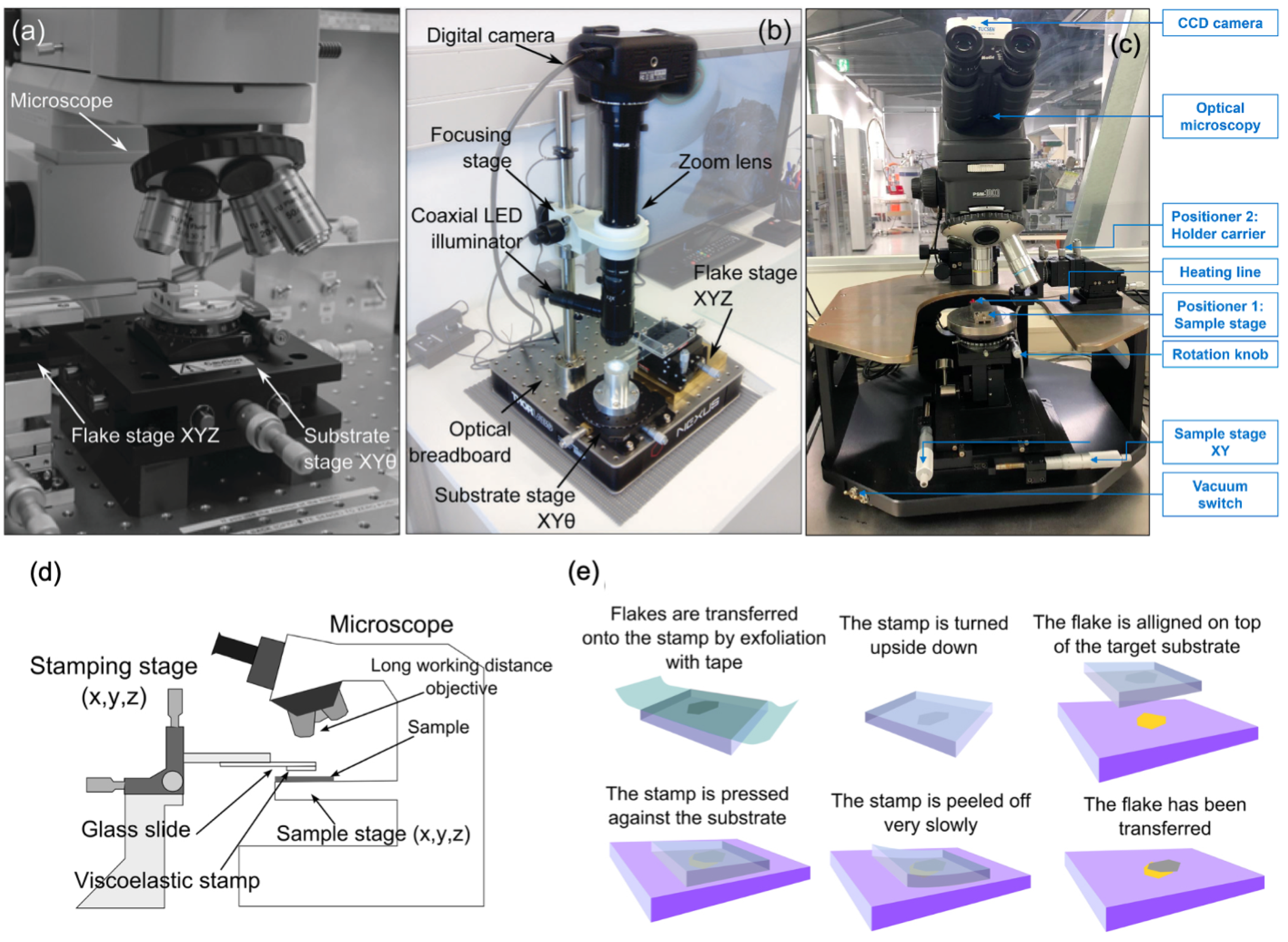
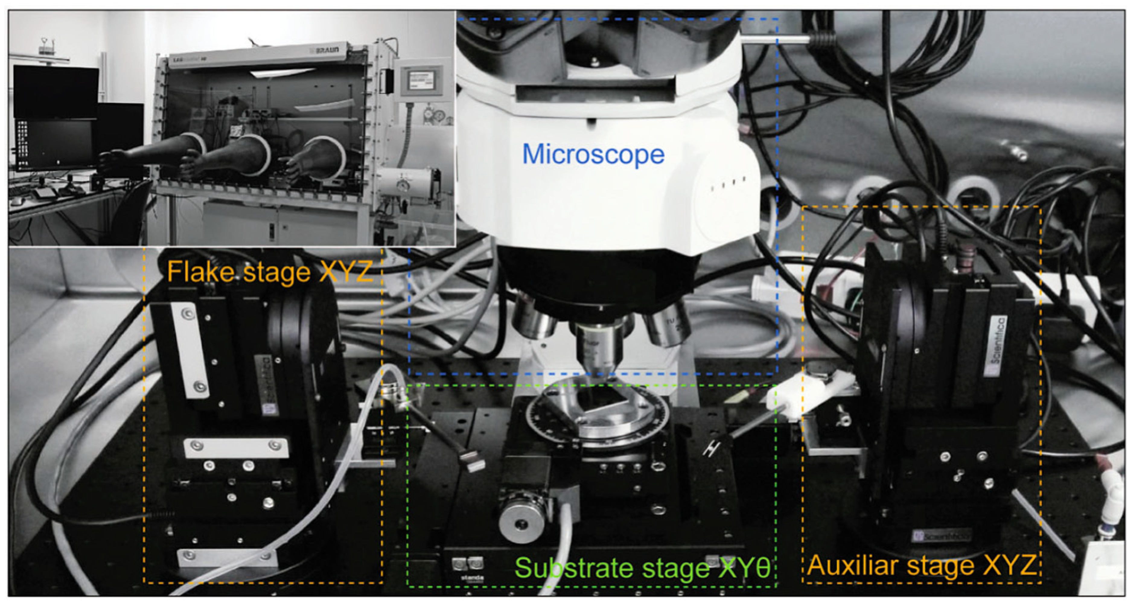
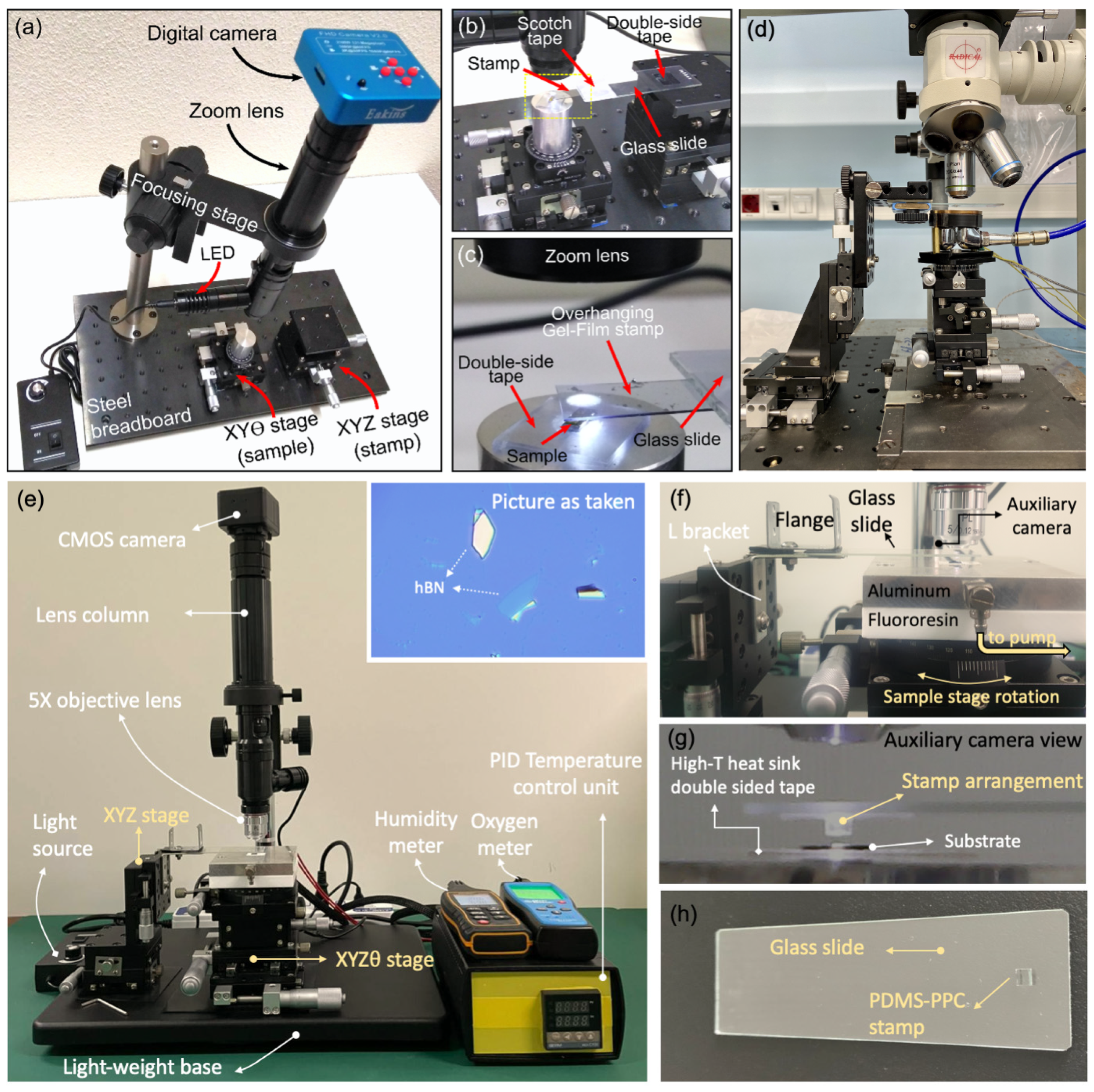
Figure 1 shows a few common ways in which the aforementioned requirements are fulfilled to successfully construct a working 2D material transfer system. Figure 1a shows a modified optical microscope system used in conjunction with an optical base and micromanipulators [6]. An alternative low-cost system, shown in Figure 1b, utilizes zoom lens configurations, which deliver satisfactory rather than optimal image quality, albeit with improved working distances [10,11,12,32]. Figure 1c shows a typical probe station setup modified slightly to function as a transfer system [21]. In later sections, the use of glove box systems is reviewed.
The transfer methods employed in a transfer system may be generally categorized into wet and dry techniques, depending on whether they use soluble sacrificial layers. Wet-transfer techniques, developed around 2010, involve water-soluble layers and PMMA for transferring thin flakes, which can lead to wrinkles and molecule adsorption, necessitating organic solvents for residue removal [56,92,93,94,95]. Dry transfer methods, in contrast, use viscoelastic polymers, like PDMS, to pick up and release 2D crystals, minimizing mechanical deformation and molecular adsorption [96,97]. An advanced dry transfer technique uses vitreous polymers, like PPC, polycarbonate, or nitrocellulose, which have tunable adhesion strengths based on temperature [98,99,100,101]. To further improve sample quality, vdW heterostructures are sandwiched between hexagonal boron nitride (h-BN) flakes, avoiding direct contact with polymers or solvents and resulting in extremely clean interfaces, albeit with increased complexity and reduced yield [97]. Figure 1d,e shows the schematic of the setup used for dry transfer and the steps involved in the deterministic placement of 2D materials onto a specified location.
Figure 1. Experimental setups for deterministic transfer. (a) Modified metallurgical optical microscope setup with long working distance objectives, featuring two linear stages: an XYZ stage for the flake/stamp and an XYθ stage for the substrate. (b) Probe station apparatus equipped with a long working distance optical microscope connected to a camera, and two micro-positioners: Positioner 1 for the sample stage, which includes a heating system and a vacuum chuck for sample stability, and Positioner 2 for the holder carrier. (c) Cost-effective setup using a zoom lens with coaxial illumination. (d) Schematic representation of the experimental setup for all-dry transfer. (e) Schematic illustrating the steps involved in the deterministic transfer of an atomically thin flake to a designated location. (a,b) Adapted from ref. [6] with permission from The Royal Society of Chemistry. (c) Adapted with permission from ref. [70]. Copyright 2020, IOP Publishing. (d,e) Reprinted with permission from ref. [96]. Copyright 2014, IOP Publishing.
Applsci 14 06341 g001

2.2. Microscope

The operator’s need for a clear view of the working area, which varies widely from 2 × 2 mm2 for flake identification, to 500 × 500 µm2 for carrying out the transfer step, and to below 100 × 100 µm2 for closer inspection of the structures, necessitates the incorporation of a microscope with varying magnification objectives (5× to 50× Plan objectives) [102]. Objectives with large working distances and mounted on a revolver head are preferred, as they facilitate focused observation and prevent the lens from contacting with the stamp holder. A comfortable working distance required during the transfer step should be greater than 5 mm, so as to ensure enough space for the glass slide containing the stamp to be inserted. These Plan objectives are widely used by research labs and commercially available 2D transfer setups (see hq2d.com, analytical-online.com, holmarc.com) and can be obtained from reputable companies, like Zeiss, Nikon, Olympus, Mitutoyo or Leica.
Whereas high-magnification (greater than 50×) objectives are crucial for inspection, they are unsuitable for transfer due to their shallow depth of field. It must also be noted that more expensive objectives, such as the apochromatic lens, are generally not a stringent requirement for the purpose of 2D material transfer. In addition, a fast (>30 fps), high-resolution (>20 MP) digital camera, and related camera software, is essential for real-time monitoring and capturing of high-quality images throughout the transfer process.
A crucial requirement for 2D material transfer is the need for independent focusing of both the stamp surface and the substrate surface. This is especially true during the moments the actual transfer is taking place. To achieve this, vertical adjustment of the objective lens is required. In typical metallurgical or inspection microscopes, the sample is focused via vertical adjustment of the sample stage, while the objective lenses remain stationary. For this reason, 2D material transfer setups work more effectively with modular microscopes designed with vertical movement of the objective lens for focusing, akin to microscopes found in probe station setups [70]. Such a setup is usually mounted on a firm stationary base with no movable sample stage, which allows the user to conveniently insert XYZ linear stages or micromanipulation accessory in the empty space between the objective lens and the base. Also helpful is the fact that the microscope arm in these setups can be detached from the base and installed on a more vibration isolated optical breadboard. While such modified (modular) microscopes from reputable manufacturers exist, and offer superior performance, more affordable alternatives (for example, MXFMS from Sunny Optical Technologies Limited, Zhejiang, China or ICM-100, from LANOPTIK Technologies Limited, Guangzhou, China) are available that are more compact and thus provide convenience for glovebox setups, a functionality that is of utmost importance for air-sensitive vdW integration. Higher quality, large working distance objectives may be installed onto these systems to improve the quality of the imaging. Additionally, stereo/zoom microscopes with single objectives and zoom functionality (see Figure 1c) serve as an effective alternative. While these systems are less costly and offer a longer working distance, they come at the expense of slightly reduced image quality.
It must be noted that the simplest and most straightforward way to build a transfer system is by using a probe station (Figure 1b). Except for their bulkiness, which makes it cumbersome to load them into a glovebox, typical probe station setups are ideal as they can be quickly converted to function as a transfer system. All that is required is the appropriate linear stage for the stamp holder and a little modification to the sample stage to enable substrate heating, if this feature is required by the transfer method employed. By default, the probe station chuck has substrate vacuum and XYθ adjustment, and the system is robust and very well vibration isolated, which helps greatly with the transfer process. The optical system is also of high quality, with the required objective lens options and camera that comes as standard (see www.signatone.com for details). For research groups that already possess a probe station, this option would be most preferred.

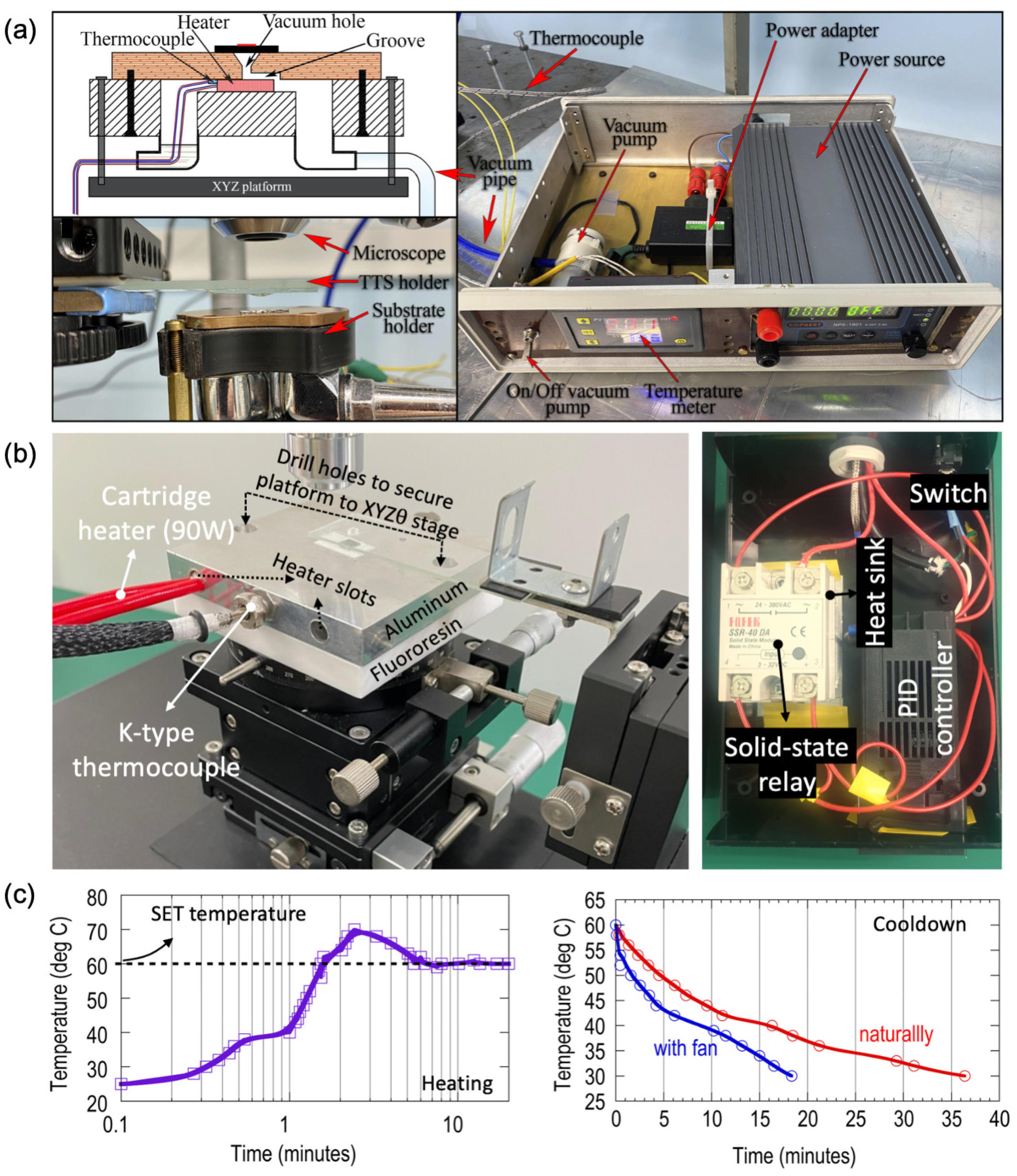
2.3. Substrate Holder Design

The substrate holder should mainly facilitate positioning with micrometer resolution along the x, y, and z axes. Additionally, for creating twisted heterostructures [103,104,105], precise rotation of the substrate in the horizontal plane is necessary. An XYZθ linear stage onto which the substrate holder can be affixed is therefore required. These are relatively inexpensive (~USD 300) and can be purchased from online sources (www.aliexpress.com). The XYZθ linear stage assembly, which carries the substrate, should also be convenient to remove when a change of substrate/flake is desired, for instance, during the vdW stacking process. Firmly attaching the XYZθ stage to the microscope base or the optical breadboard might be disadvantageous as the entire stamp assembly has to be moved out of the way before sample exchange is possible. For this reason, it is advisable to use substrate holders with magnetic bases [81] or by placing them on single-axis slides that are secured to the optical board. These slides are readily available for purchase online (www.aliexpress.com) and enhance the overall functionality of the transfer setup by enabling fast substrate changes when required. A crude, low-cost approach is also possible, as demonstrated in [83], where authors simply place the linear stage on top of rubber vibration damping pads and manually move out the stage by hand, as needed. It is worth noting that all manual motion and rotation stages can be upgraded to motorized ones, which is advantageous for glovebox operation and helps mitigate vibrations [85,106].
Turning to the construction of the substrate holder, the two key requirements are that of substrate heating and sample vacuum. The most popular vdW pick up technique, popularly dubbed as the “hot pick-up” technique [97], relies on the varying polymer sensitivity with temperature. A reliable way to provide substrate heating is therefore critical. This requires a heating element that can be incorporated into the substrate holder plate/assembly, thermocouples to measure the substrate temperature, and a temperature controller to set, adjust and monitor the substrate temperature. A strong enough vacuum suction to secure the sample in place is also vital. Commercially-available vacuum chuck hot plates (see www.tceramics.com) or similar chucks used in probe stations and wire-bonder setups may be used for this purpose. However, they are often expensive, bulky, and hard to integrate with the XYZθ linear stage. A custom-built substrate stage is therefore often preferred by researchers. Martanov and colleagues [102] demonstrated the use of a PC Motherboard water-block as the chuck replacement, and the space inside the chamber of the water-block was utilized to install the heater and thermocouples, and all the necessary routing for the heating and vacuum lines are achieved using the water entrance and exits of the water-block (see Figure 2a). Buapan et al. [83] followed a different approach, wherein the substrate holder comprised of a 12-mm thick aluminum block machined in appropriate locations to conveniently house the cartridge heaters, thermocouple and the vacuum port (Figure 2b). A thermally insulating fluoro-resin plate, matching the dimensions of the aluminum plate, was placed between the aluminum plate and the XYZθ stage. The fluoro-resin plate isolates the hot plate from the XYZθ stage below, preventing overheating of the heaters and PID controllers and safeguarding the XYZθ stage from potential damage. Vertically aligned drill holes are then made at precise locations on both plates, followed by the use of insulating screws to secure them to the XYZθ stage.
For the assembling of electronic components, the authors of [102] used a box in which a low-cost diaphragm pump is installed as vacuum, in addition to a PID controller kit for temperature sensing. The authors reported that the PID system was slow to respond and therefore utilized a laboratory power source for enabling substrate heating. A common cell phone adaptor was used to power the pump and the temperature meter.
In [83], electrical connections to the cartridge heater and thermocouple are facilitated by a lightweight PID controller kit available online at an affordable cost. The PID controller, in conjunction with a solid-state relay, regulates the power output to the heaters. After wiring, the components are neatly packed into an electronic enclosure box The completed unit was reported to occupy a small footprint and weighed a mere 300 g, significantly lighter than a typical laboratory bench power supply. The authors also tested the typical heating and cooling responses of the PID controller and reported that a steady state at a temperature of 60 °C is achieved in approximately 5 min, while cooldown to room temperature was slower but can be expedited with the aid of a small cooling fan (see Figure 2c). The authors additionally proposed that faster cooling could be achieved with additional installable options, such as water- or air-cooling tubes or a heat sink material placed on top of the hot plate.
Alternatively, a Peltier module, as previously suggested by Uwanno et al. [107], can be employed to achieve both heating and cooling by simply reversing the voltage direction. This module, readily available from www.aliexpress.com, can replace the use of resistive heaters. While the Peltier component offers faster response times, it is not compatible with vacuum fixation, necessitating the use of double-sided adhesive tape. The operating temperature range for the Peltier element is also more limited, spanning from 10 °C to 80 °C.
While the authors of [83] demonstrated the integration of the sample vacuum feature in the substrate holder, they did not actually utilize this feature in their work. Instead, the authors secured the sample to the stage using a high-temperature, double-sided thermal tape suitable for hot-plate temperatures up to 120 °C, thus offering a simple and effective solution without risking melting or contamination of the substrate underside. The authors also suggest that the use of pumps could result in vibrations that can negatively affect the 2D material transfer process.
It has also been suggested [102] that employing computer control, akin to the approach used by www.hqgraphene.com, is likely to enhance the transfer process, rendering it faster and more manageable. This approach appears viable particularly for mass production of van der Waals heterostructures. However, such automation may not be necessary for a small scientific group with restricted measurement resources, where the primary constraints lie in time-consuming stamp preparation, material exfoliation, and exploration.

2.4. Stamp and Holder Design

The main function of the stamp holder assembly is to house the glass slide containing the transfer stamp. Typically, a thin layer of PDMS is used as the stamp when following the viscoelastic stamping method [6], whereas stacks of PMDS/PPC are used when a hot pick-up technique [97] is desired, as the PPC layer enhances the adhesion of the 2D material to the stamp.
The PDMS stamp may be in the form of a drop [102] or, more commonly, in the form of a viscoelastic sheet, which can be easily obtained with varying sheet thickness and properties from companies like GelpakTM. The viscoelastic PDMS stamp can also be readily prepared in the laboratory setting using Sylgard 184 elastomer, which basically consists of a pre-polymer and curing agent [83]. Ref. [108] and online video tutorials (https://www.youtube.com/watch?v=SLWmMIAG-oA, accessed on 1 June 2024) are available for a quick reference on how to make a PDMS film.
If the hot pick-up method is used, the prepared film is generally spin-coated with PPC to obtain a uniform coat. Typically, to ensure uniform coating, the PDMS film has to be placed at the center of the glass slide. However, this causes a loss of wiggle room for the stamp assembly, which may end up contacting the linear stages while performing the transfer. To avoid this undesirable outcome, several simple solutions can be implemented, e.g., a larger glass slide [109], or extending the length of the glass slides with a second one [106], or, most commonly, by a placement of the stamp on the edge of the glass slide [83]. In the report by Buapan et al. [83], the uniform coating of the PPC layer is achieved via spin coating of a small microscope coverslip laden with the PDMS film. The PDMS/PPC stack is then easily separated from the coverslip and attached to the transfer glass slide. Alternatively, the issue of lack of wiggle room can be circumvented by using a standalone manual rotation stage (from Thorlabs) affixed onto a XY linear stage [6,81].
For installation of the glass slide to the linear stage, simple methods, such as using cheese plates for photography [102], or general-purpose L brackets [83], or, as commonly used, double-sided sticky tape, may also be employed. Some consideration should also be given to the choice of the XYZ stage design, which comes with vertical or horizontal guide plate configurations. The sticky tape option is easy to implement with a horizontal guide plate [81], but the maximum height of the stamp assembly with respect to the substrate stage is reduced and this might necessitate adding extra parts to obtain the correct height. The use of a vertical guide plate allows one to increase the level of the glass slide so that the tall height of the substrate stage (XYZθ) can be compensated for and makes the transfer process more comfortable to carry out [83].
The sample holder should have a minimum of x- and y-degrees of freedom. The additional z-degree of freedom is necessary only if the objective lens assembly is stationary. Nonetheless, having additional degrees of movement is always beneficial, for instance, when the stamp assembly needs to be changed/removed.

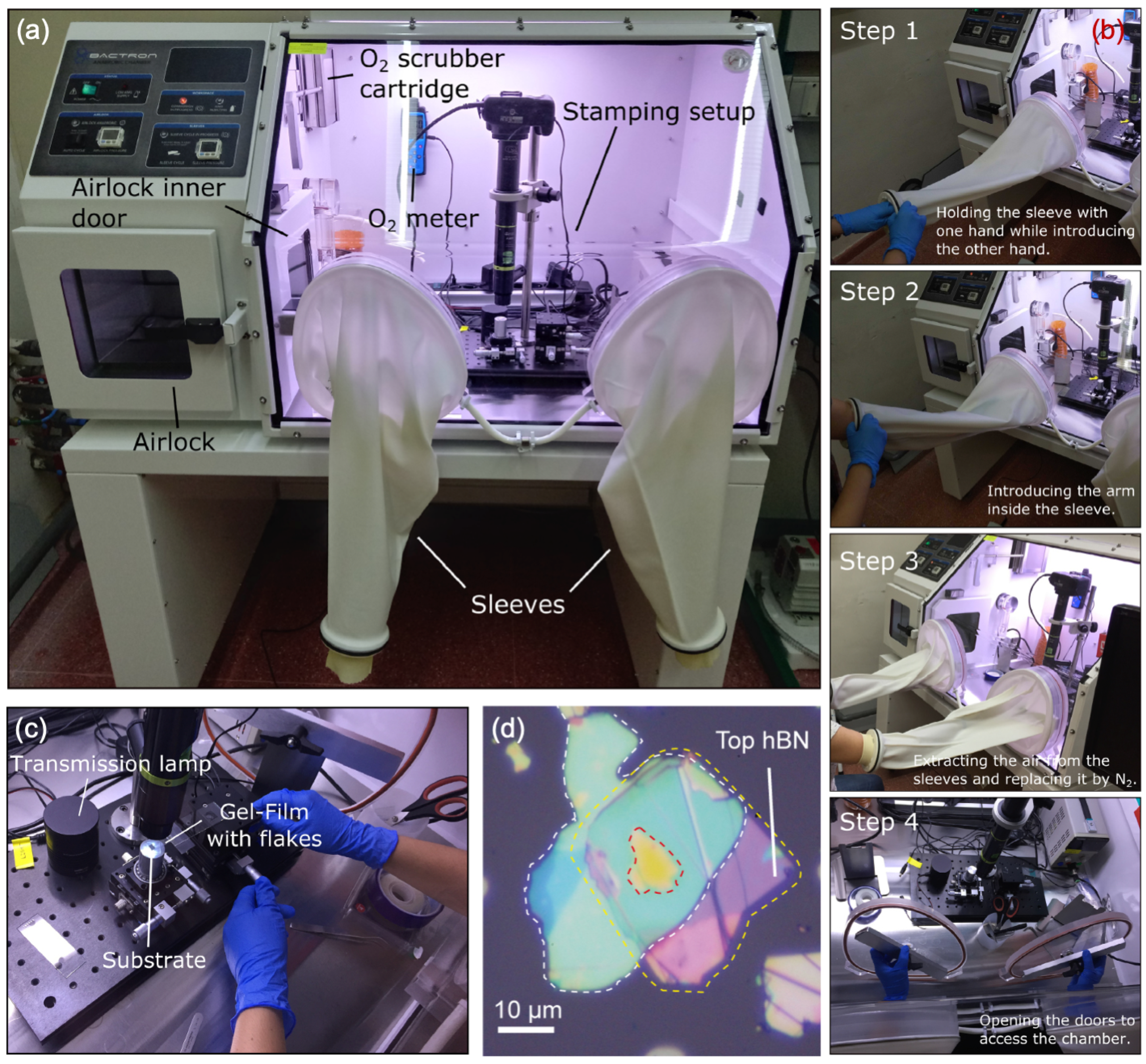
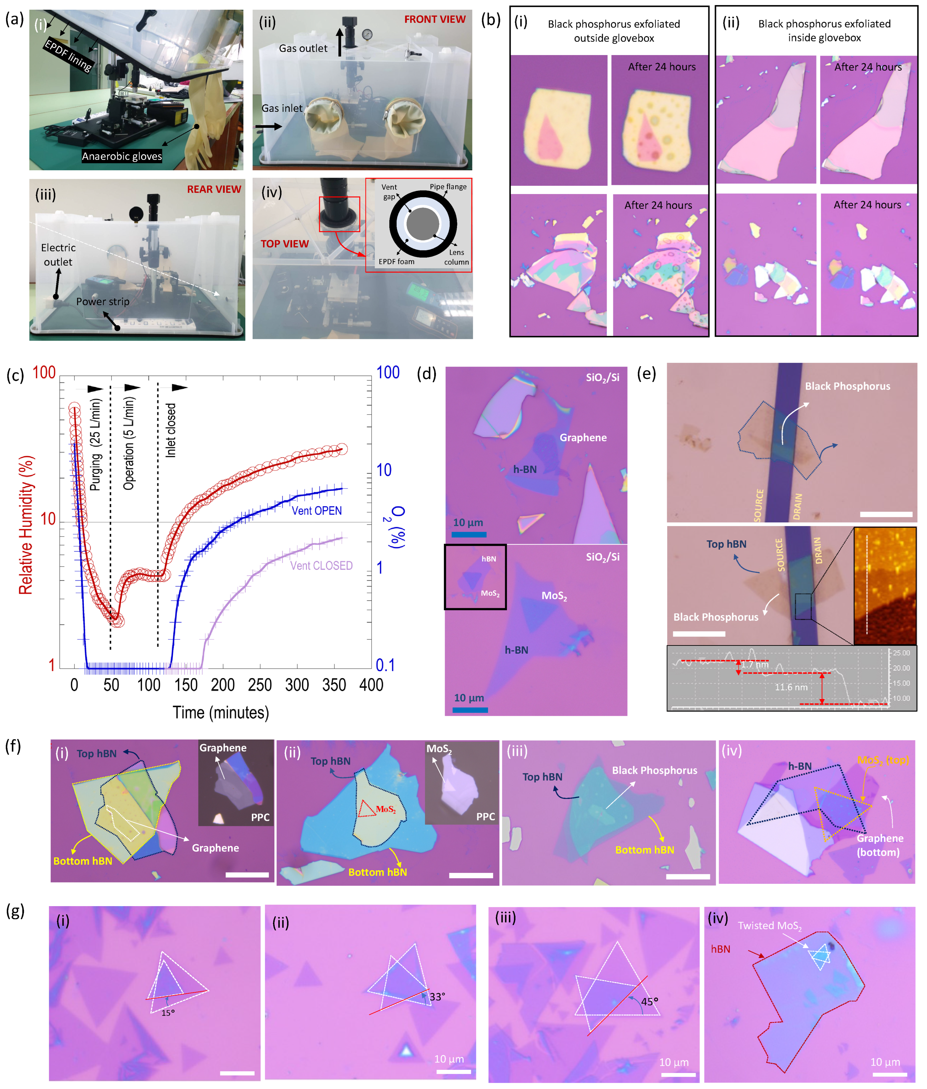
3. Transfer Setup with Glovebox Integration

While it is true that deterministic placement methods have enabled the fabrication of 2D-based heterostructures exhibiting record high electronic performance and the observation of intriguing physical phenomena, there are two main challenges that still need to be addressed. One is the challenge posed by largely susceptive interface quality [109,110,111,112], and the other is the addressing of the difficulty associated with handling of air-sensitive 2D materials [113,114].
It is known that even stable 2D materials like graphene are prone to adsorbate contamination. The source of contamination may arise from moisture, gases and/or hydrocarbons. Fortunately, these contaminants tend to segregate into small pockets, commonly referred to as bubbles/blisters, leaving behind micron-sized clean areas. This self-cleaning mechanism has enabled heterostructures based on graphene and other stable materials, like h-BN and MoS2, to have quality comparable to their MBE analogues, although the device sizes are restricted to the micron-scale. Cross-sectional studies [113,114] on various heterostructures have revealed that only a select few materials, such as graphene, h-BN, MoS2, WS2, and NbSe2, exhibit the expected interlayer spacing for a defect-free idealistic interface predicted by density functional theory (DFT). Conversely, most other materials display increased interlayer distances, likely to be due to impurities and defects in the atomic structure at the interface. As a result, the formation of layered crystals, of which there are numerous, are prone to surface contamination and modification when exposed to air. These detrimental effects are present even if one of the layers forming the heterostructure is air stable. This is because, while in bulk crystals these effects are only seen on the top few atomic layers, when exfoliated down to the level of a single atomic layer (or few), these materials experience significant loss of quality, which directly impacts interface homogeneity, and as a result the electronic quality suffers in the formed heterostructures [111].
The other important problem that needs to be addressed is the handling of materials that tend to degrade quickly when exposed to air. A well-known example is found in the exfoliated flakes of black phosphorus, distinguished by its unique puckered structure that imparts strong anisotropy in mechanical and transport properties, contrasting with graphene and transition metal dichalcogenide (TMD) 2D materials. This distinctive mechanical anisotropy holds promise for applications, such as nanomechanical resonators, thermoelectric devices, and motion sensors, offering tunable functionalities inaccessible to isotropic materials [115]. Unfortunately, the strong hygroscopic surface of 2D black phosphorus readily attracts moisture and leads to its degradation, as confirmed by Atomic Force Microscope (AFM) findings [116], and by various reports of its electronic mobility degradation [116,117,118]. Similarly, superconducting material niobium diselenide tends to oxidize upon exposure to air, hindering the fabrication of ultrathin devices [113].
The aforementioned challenges can be addressed by performing the heterostructure stacking process inside an inert atmosphere, which is commonly facilitated by a glovebox. Within the glovebox, all important steps of the heterostructure formation, i.e., the exfoliation, transfer, and encapsulation, can be carried out. It has been demonstrated that the pristine electronic properties of air-sensitive materials, like black phosphorus or niobium diselenide, can be preserved when they are fully encapsulated between layers of h-BN, resulting in high carrier mobility and reliable FET behavior in black phosphorus, and the observation of superconducting transition in niobium diselenide [113,119]. The observation of high electronic mobilities exceeding 15,000 cm2V−1s−1 and a fully developed quantum hall effect in encapsulated indium monoselenide [114] is yet another important example showcasing the advantage of forming heterostructures in a protected environment. Layer-dependent ferromagnetism has been demonstrated in mono and few layers of CrI3 [120]. Furthermore, the encapsulated devices demonstrated robust stability when exposed to air for prolonged periods of time.
It is therefore clear that isolation and transfer of 2D materials in an inert atmosphere setting has provided a unique platform for the exploration of 2D materials. This development has opened the door to numerous 2D materials that were previously inaccessible due to degradation before their properties could be measured.
Figure 3 illustrates how a deterministic transfer setup, based on a modified microscope (as shown in Figure 1a), can be integrated within a glovebox. However, in order to effectively perform the transfer within such a commercial, state-of-the-art glovebox unit, the linear stages have to be motorized and controlled from outside the glovebox using joystick controls or a computer [6,70,85]. This is mainly because the standard gloves provided in these systems are very thick, rendering them difficult to use in manual operation mode by a user, where mechanical exfoliation, and substrate, microscope and manipulator handling, all need to be carried out wearing thick gloves. While the motorization of the stages enhances the accuracy of the transfer and the technical capability of the transfer system, it also adds to cost and complexity.
The problem associated with thick gloves was later resolved by the design of a gloveless glovebox transfer setup by Gant et al. [82]. In their work, the authors demonstrated that the user could carry out all the critical steps of the transfer process with his/her bare hands, similar to how the process would normally be performed in ambient air conditions outside the glovebox. This was made possible as their system made use of sealed doors that could be opened via insertion of hands through sleeves, followed by pumping down and purging with nitrogen gas. Figure 4a shows a photograph of the gloveless anaerobic chamber used by Gant et al. Figure 4b shows the various steps needed to introduce the hands inside the chamber, and Figure 4c shows a photograph of the user operating the transfer system inside the glovebox chamber. The effective purging of the main chamber was demonstrated using oxygen scrubbers. The authors demonstrated the functionality of their transfer setup by showcasing the deterministic transfer of a h-BN encapsulated black phosphorus flake (see Figure 4d) and investigating the stability of thin black phosphorus and perovskite flakes when exfoliated within the anerobic chamber.

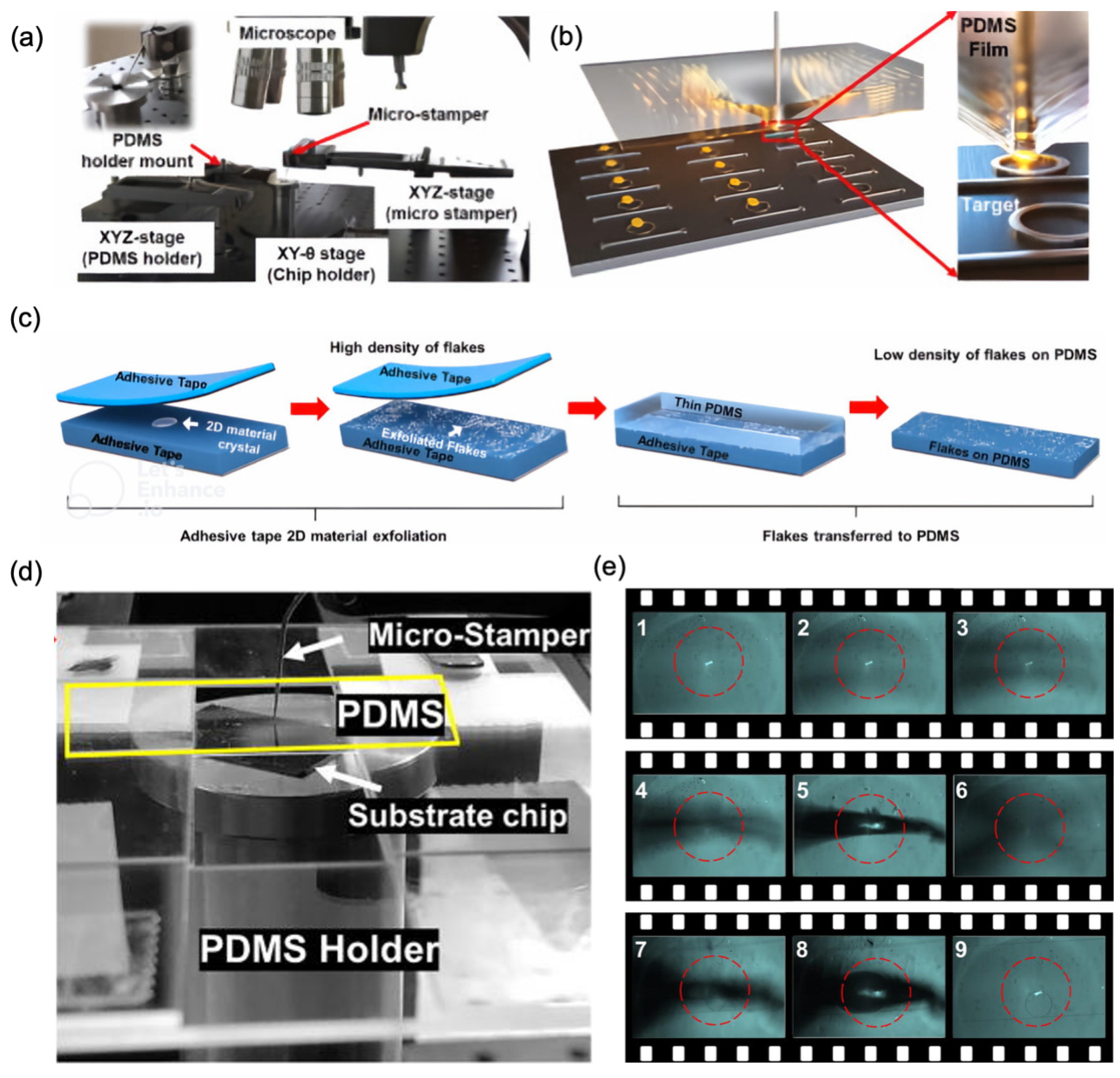
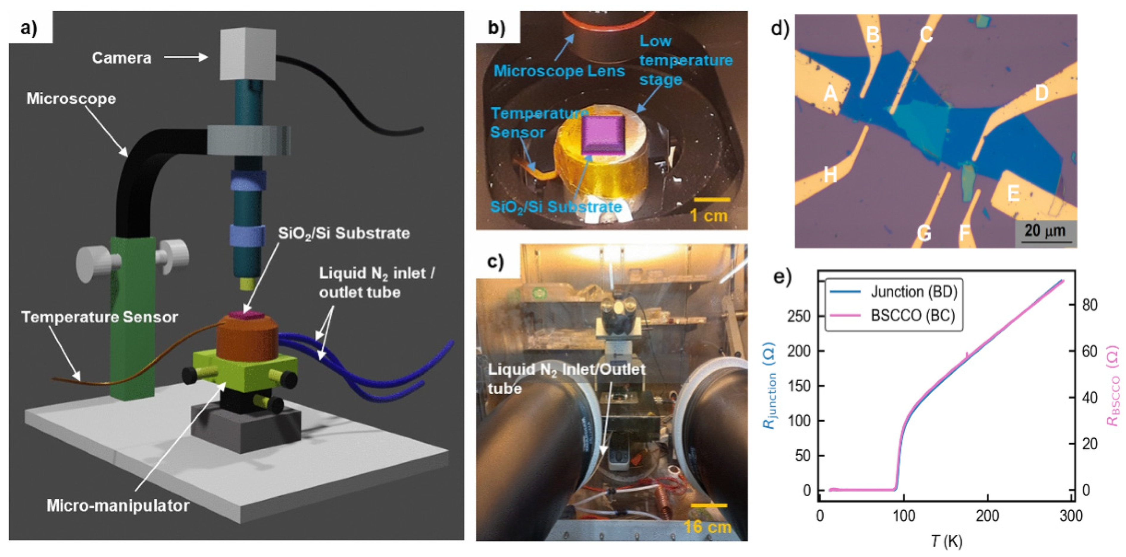
4. Cost-Effective Transfer Setups

Typically, the experimental setups used for the deterministic transfer and stacking of 2D materials are very expensive. The high cost is generally associated with the use of precision optics and mechanical components to achieve a high level of vibration isolation. A typical example of such system can be found in the earlier work of Frisenda et al. [6], in which the authors demonstrated the all-dry viscoelastic stamping technique for stacking of 2D materials. In their work, a high-quality optical microscope (Olympus BX 51, Evident Corporation, Tokyo, Japan) and a digital camera (Olympus DP25, Evident Corporation, Tokyo, Japan), supplemented with large working distance optical objectives and a three-axis micrometer stage to accurately position the stamp, are used. The typical cost of such a setup could easily exceed $20,000, due to the high cost of the microscope.
The very first reports of a moderately cost-effective transfer setup were also reported in the supplementary section of Frisenda et al. [6]. The reported cost of their custom-designed setup was ~7000 Euros, with the significant cost reduction coming from the replacement of high-end optics with zoom lens. The bulk of the remaining cost is from the use of an expensive optical base and magnetic clamping systems. It must be noted that the viscoelastic method did not require substrate heating, so the reported transfer system was not built with a heating stage and was thus simpler in its design. See the supplementary section of [6] for design details and associated costs.
Today, versatile systems with substrate heating and vacuum are also available commercially. For instance, www.hqgraphene.com provides a transfer setup that costs approximately USD 21,000. As noted earlier, transfer systems may also be based on retrofitting probe stations [70] and already existing mask aligners (Karl Suss MJB-3, SUSS MICROTEC SE, Garching, Germany used by Zomer et al. [121]). While these options may appear to be cost-effective for research groups already having access to such equipment, they are a non-starter for young researchers working in small- to medium-sized laboratory settings where there is no access to such sophisticated systems. Moreover, these transfer systems end up being bulky and immobile and having a large footprint, making their practicality questionable.
In recent years, several further advancements have been made in designing transfer systems that are truly low-cost (<USD 1000) and their effectiveness has been proven with the successful assembly of high-quality heterostructures. Zhao et al. [81] built a low-cost setup (Figure 5a) for under 900 Euros. The setup employed in their work was very similar to the one reported earlier [6], but the significant cost reduction was achieved by using much lower cost optical breadboards and parts purchased from online providers, like Amazon and AliExpress. The effectiveness of the transfer setup was demonstrated by transferring a thin InSe flake onto prepatterned gold electrodes. The researchers were also able to transfer a hexagonal boron nitride (hBN)-encapsulated InSe flake using the same setup.
Yet another cost-effective system, built using a low-cost modular microscope along with the option of a heated sample stage, was reported by Martanov et al. [102] (Figure 5b). The use of a heated sample stage allowed the authors to perform the hot pickup transfer, and using this method they demonstrated the successful creation of sandwiched hBN/WSe2 heterostructures. The cost of the system was reported to be under USD 1000.
As discussed in the previous section, the authors of Gant et al. [82] have gone a step further and demonstrated the creation of hBN-encapsulated black phosphorous (BP) heterostructures in an inert-atmosphere gloveless anaerobic chamber (see Figure 4). In their work, the transfer steps were carried out using a transfer setup based of a high-quality zoom lens set from Edmund Optics but with no heating stage (similar to Zhao et al. [81]. However, the integration of the transfer system into a commercial anaerobic chamber meant that the total cost of the system was very high (~USD 23,000 as reported [82]).
Upon briefly reviewing the above works, a few limitations may be noticed. For instance, despite the use of XYθ manipulators, the main usefulness of this type of stage, namely, the formation of twisted 2D heterostructures, was not demonstrated in these reports using a low-cost setup. Second, a low-cost setup can benefit greatly from a light-weight PID-controlled power supply, instead of conventional laboratory power sources, to drive the heating stage. This helps with lowering cost, increases portability, and allows for quick and easy implementation of the hot pickup process. Third, the versatility of the system to cover other transfer techniques, such as the recently popular capillary-force-assisted wetting PDMS technique [122,123,124], was not adequately studied using low-cost setups. Finally, although the possibility of incorporating such low-cost setups into commercial glovebox systems has been explored, these units are way too expensive for implementation in budget-restricted research groups. These proved an impediment for researchers eager to work with air-sensitive 2D materials.
The abovementioned shortcomings were later addressed in the work of Buapan et al. [83] in 2021. In their study, the authors developed an in-house, low-cost transfer system (Figure 5c) using readily available components from online stores. Their system is both budget-friendly and compact, offering features such as PID-controlled substrate heating, thermal isolation for the sample stage, XYZθ and XYZ manipulators, and sample vacuum. Additionally, they illustrate how the proposed portable transfer setup can be easily integrated with a do-it-yourself (DIY), cost-effective (∼USD 170) humidity (<4%)- and oxygen (<0.1%)-controlled inert-atmosphere glovebox (Figure 6). This modification enables quick adaptations for isolating and controlling environments during the exfoliation and transfer of sensitive 2D materials. The authors demonstrate that their DIY glovebox is capable of reducing the RH levels within the working area from 63% to less than 5% in just under 10−15 min of N2 gas purging, and that, during this time, the O2 level had already dropped from 21% to less than 0.1% (or 1000 ppm). The remarkable sealing performance of the DIY glovebox was further emphasized by demonstrating that the rate of RH (and O2) increase post shutting off the inert gas supply is seen to be at least a few orders of magnitude slower than the rate of the initial decrease. With the vent in the closed position, the RH and O2 levels were shown to remain at very low levels for several hours post-operation of the glovebox. The efficacy of the DIY glovebox was validated by demonstrating the extended stability of freshly exfoliated BP flakes, their encapsulation between thin hBN layers, and the fabrication of source- and drain-contacted BP devices with a protective hBN top layer (see Figure 6).
Furthermore, Buapan et al. evaluated the effectiveness of their low-cost setup by testing various transfer techniques for 2D materials, including hot pickup, wetting PDMS technique, and a combination of both. They demonstrate the advantages of the combination approach, particularly for stacking specific 2D material candidates. The versatility of their system is showcased through successful creation of various structures: graphene on hBN, MoS2 on hBN, twisted MoS2 on SiO2 with various twist angles, and twisted MoS2 on hBN, were created using the capillary wetting transfer approach. hBN-encapsulated graphene, hBN-encapsulated MoS2, and hBN-encapsulated BP, were assembled using the hot-pick transfer method. Using a combination approach of both hot pick-up and capillary wetting, the authors realized a vertical tunneling structure of MoS2-hBN-graphene. Photographs of final device structures are shown in Figure 6.

5. Advanced Setups

In this section, we highlight recent literature reports on advanced setups for the effective transfer of 2D materials and the formation of van der Waals (vdW) heterostructures. The advancements are primarily in two key areas: the development of “cleanroom in a glovebox” systems, where most, if not all, stages of device fabrication are performed entirely within a controlled glovebox environment, and the development of robotic searching and assembly systems that circumvent the challenges associated with manual methods discussed in previous sections. These advancements are crucial for the future of vdW devices and technologies. While 2D material searching and stacking have become more common, contamination issues during fabrication steps, such as lithography, plasma etching, metal evaporation, sample characterization and probing, remain significant. These issues can degrade sample quality, especially for air-sensitive materials, as samples are inadvertently exposed to the ambient environment between fabrication steps.
Similarly, robotic automation setups [73,85] for 2D material searching and stacking play a pivotal role in the fabrication of vdW heterostructures. Traditionally, this process involves manual exfoliation to obtain the desired flakes and manual transfer to build the heterostructures. This manual approach is time-consuming, labor-intensive, and highly dependent on the operator skills, leading to variability in the quality of the resulting structures. Additionally, performing these tasks inside a glovebox system, necessary to maintain an inert atmosphere for certain sensitive materials, further complicates the manual process.
Automation addresses these issues by utilizing robotic systems equipped with machine vision and artificial intelligence (AI). These systems can identify and select the optimal flakes based on predefined criteria, significantly reducing the time and effort required for material preparation. Furthermore, automated transfer systems ensure consistent and precise placement of flakes, minimizing human error and improving the reproducibility of the heterostructures. The integration of AI and automation in this process allows for the rapid assembly of complex vdW heterostructures, which are essential for various advanced applications in electronics, photonics, and quantum technologies.

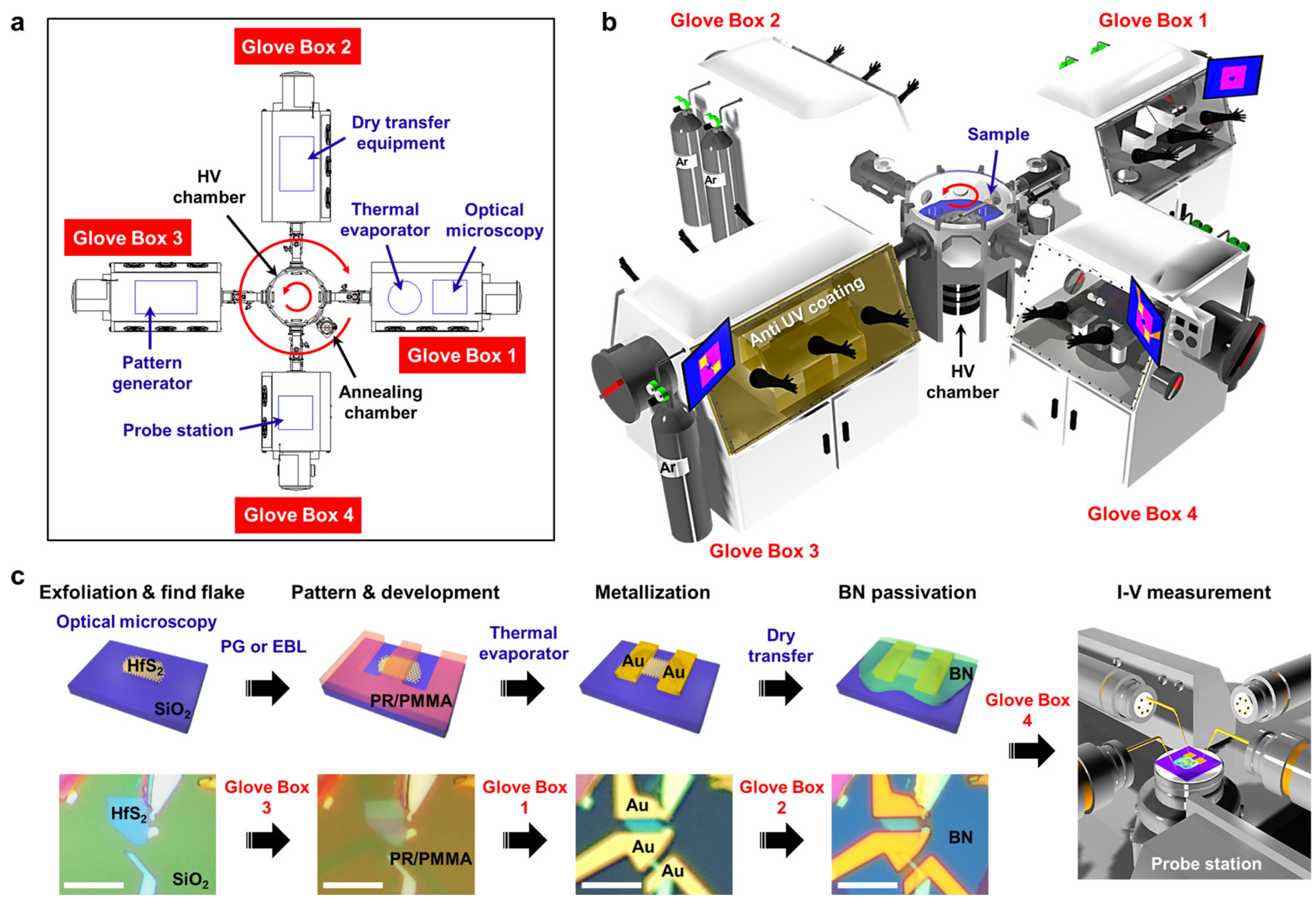
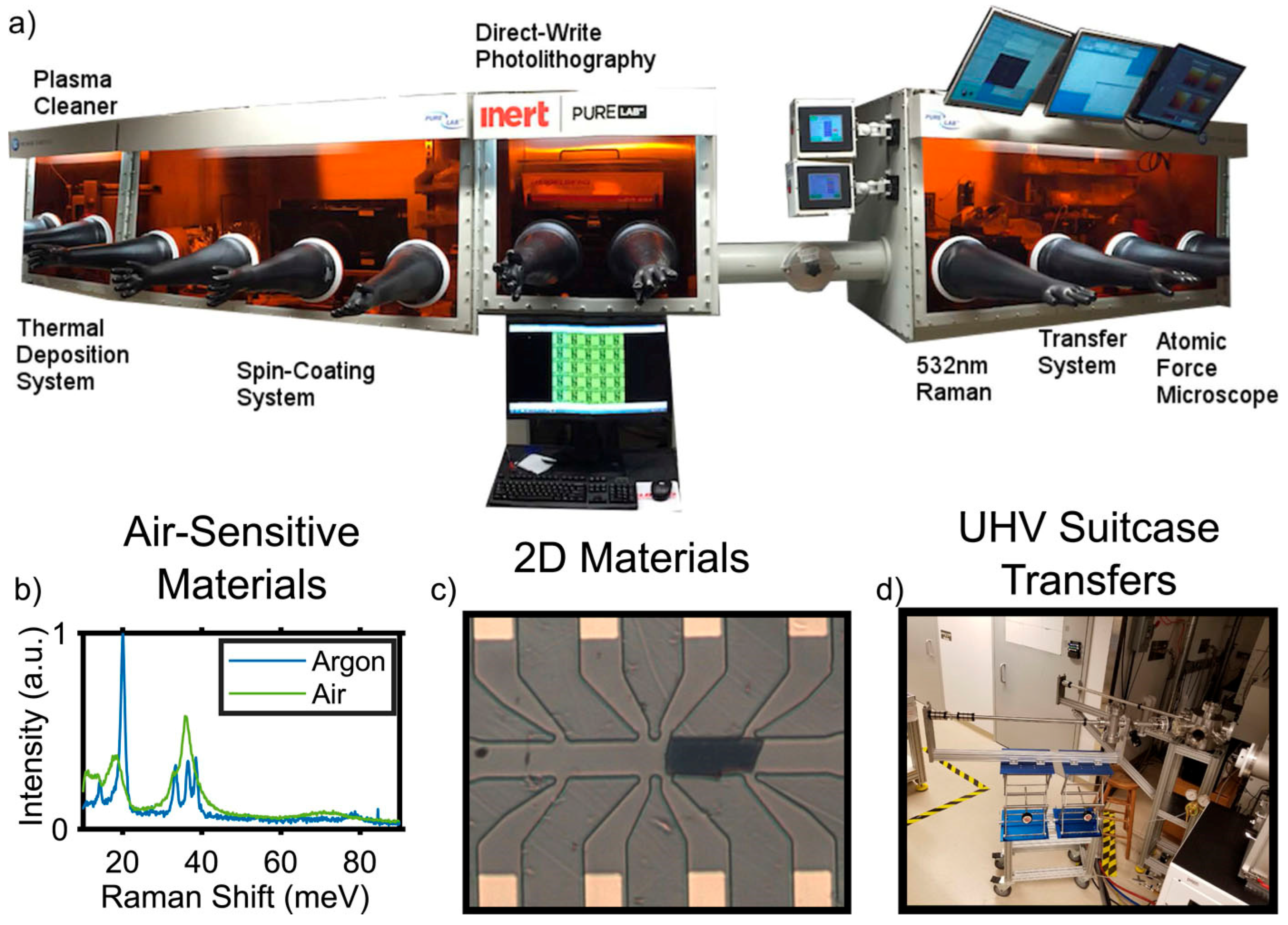
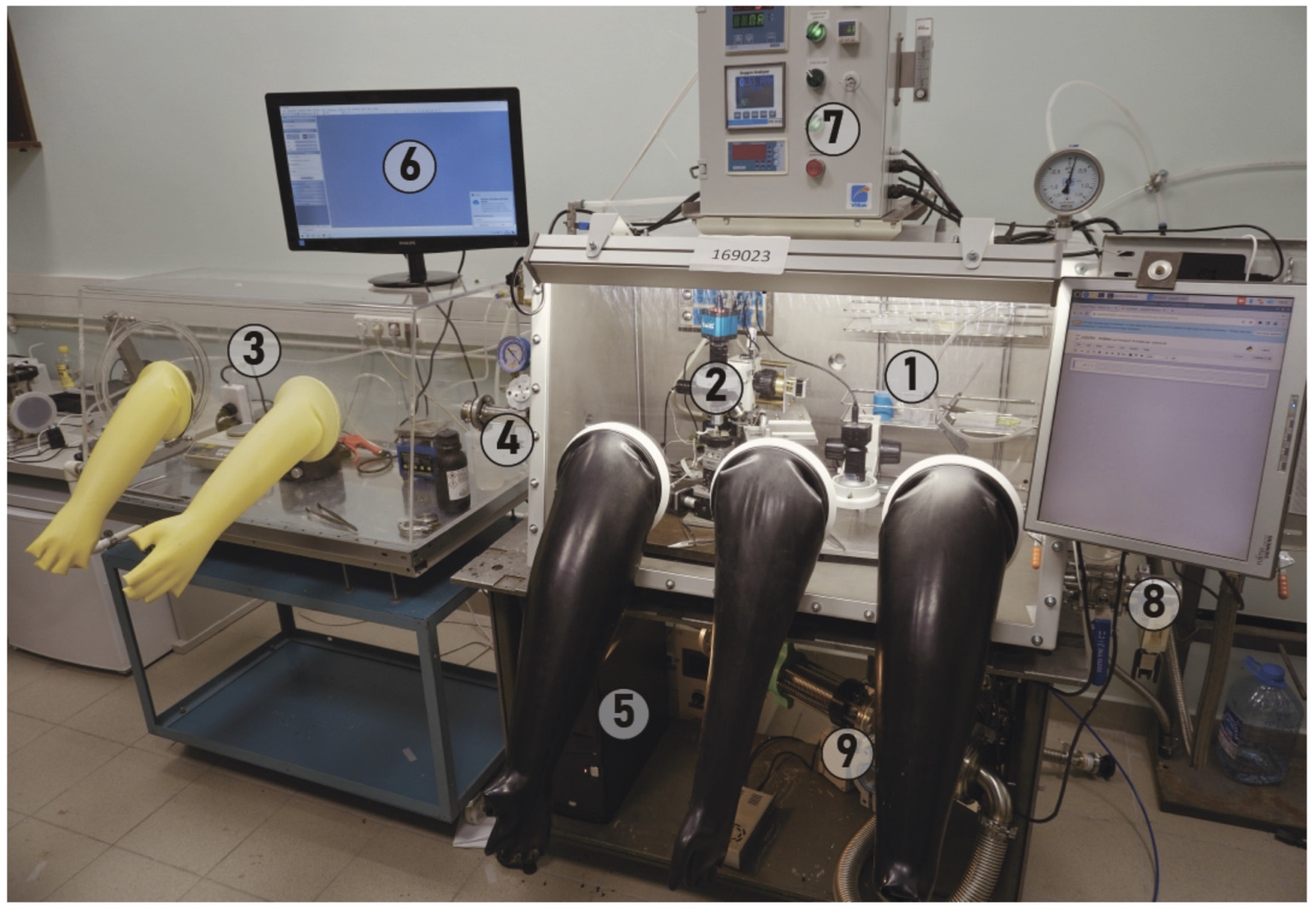
5.1. “Cleanroom in a Glovebox” Setups

In the research work of Chae et al. [84], a vacuum cluster system integrated with several gloveboxes has been developed to enable oxygen- and moisture-free fabrication and characterization of devices, particularly those involving air-sensitive materials. This system comprises four interconnected gloveboxes linked to a high-vacuum chamber with a robotic arm, facilitating seamless transfer of samples without air exposure. The gloveboxes are filled with high-purity argon gas, maintaining moisture and oxygen levels below 1 ppm, crucial for preventing sample oxidation during fabrication processes. The gloveboxes are equipped with various tools: an optical microscope and thermal evaporator in Glovebox 1, a dry transfer system in Glovebox 2, a pattern generator in Glovebox 3, and a probe station in Glovebox 4, alongside additional equipment, like a spin-coater and hot plates (Figure 7). The gloveboxes are connected by buffer cluster and terminal chambers. This setup ensures a controlled environment for each step, maintaining a pressure of 10−6 Torr in the cluster chamber. Utilizing this system, few-layer hafnium disulfide (HfS2) field-effect transistors (FETs) were fabricated, demonstrating high switching ratios (Ion/Ioff ≈ 107) and low hysteresis at room temperature. Despite the potential of HfS2 in optoelectronic applications due to its reasonable mobility, bandgap, and high photoresponsivity, the material showed rapid structural degradation when exposed to air, highlighting the necessity of the vacuum system to preserve its intrinsic properties.
The research article A Cleanroom in a Glovebox by Gray et al. [86] describes the creation of a hybrid system that merges the benefits of traditional cleanrooms and gloveboxes to fabricate and characterize sensitive materials in an inert argon atmosphere. This innovative setup (Figure 8) includes two main chambers: one for lithography equipped with precision tools, like the Heidelberg μPG101 Direct-Write system, and another for characterization featuring advanced instruments, such as the WITec alpha300R confocal Raman system and a Nanomagnetics ezAFM. The glovebox is designed to maintain extremely low levels of oxygen and water through continuous argon recirculation, passing the gas through a copper column to adsorb contaminants and HEPA filters to remove particulate matter, achieving particle counts equivalent to a class 100 cleanroom. A custom-built antechamber connects the two main work chambers, allowing seamless sample transfer without air exposure. Additionally, an intermediate chamber at the back of the glovebox interfaces with an ultra-high vacuum (UHV) suitcase, enabling the system to connect to various UHV systems, like molecular-beam epitaxy and scanning tunneling microscopy, for advanced material analysis. The efficient maintenance of an inert atmosphere, with oxygen and water levels kept below 1 ppm, allows for high-quality material fabrication and characterization. The user-friendly design requires minimal training and no special attire, operating effectively for four years without needing filter replacements. This system provides a versatile and cost-effective solution for high-quality material fabrication and characterization, crucial for advancing research and training in quantum materials.
In more recent work by Duleba et al. [87] in 2023, the authors introduced a cost-effective (~USD 32,000) and compact microfabrication setup specifically designed for the manipulation of 2D materials that are unstable in ambient conditions. Central to their approach is the use of a glovebox system with an inert nitrogen atmosphere containing less than 20 ppm oxygen. This system enables the entire fabrication process, including optical contact mask lithography, metal evaporation, and electric measurements, to be conducted without exposing the materials to air.
The glovebox setup, shown in Figure 9, consists of two interconnected gloveboxes: one for “clean” processes and one for “dirty” processes. The clean glovebox houses a custom-built transfer lithography machine equipped with motorized XYZθ stages and a metallographic microscope for precise assembly and lithography operations. It also includes a storage area for substrates, crystals, and tools, as well as a load lock for transferring samples to a connected cryostat for measurements. The dirty glovebox, used for photoresist application and development, features a spin-coater, a hot plate, and chemical storage, all designed to minimize contamination and overheating. The authors emphasize the modularity and affordability of their setup, highlighting the use of off-the-shelf components and home-built solutions to keep costs low. For instance, their lithography machine combines a standard metallographic microscope with a homemade mask aligner capable of achieving a resolution below 2 µm. The integration of this setup with vacuum chambers for metal deposition and plasma processes allows for a seamless fabrication workflow entirely within the inert atmosphere.
Their demonstration of the system’s capabilities includes the fabrication of black phosphorus (BP) heterostructures encapsulated in hexagonal boron nitride (hBN) and the subsequent analysis of their degradation when exposed to air. Overall, the reported glovebox system represents a significant advancement in the field of 2D material fabrication, providing a practical and scalable solution for laboratories aiming to explore the properties and applications of air-sensitive 2D materials.

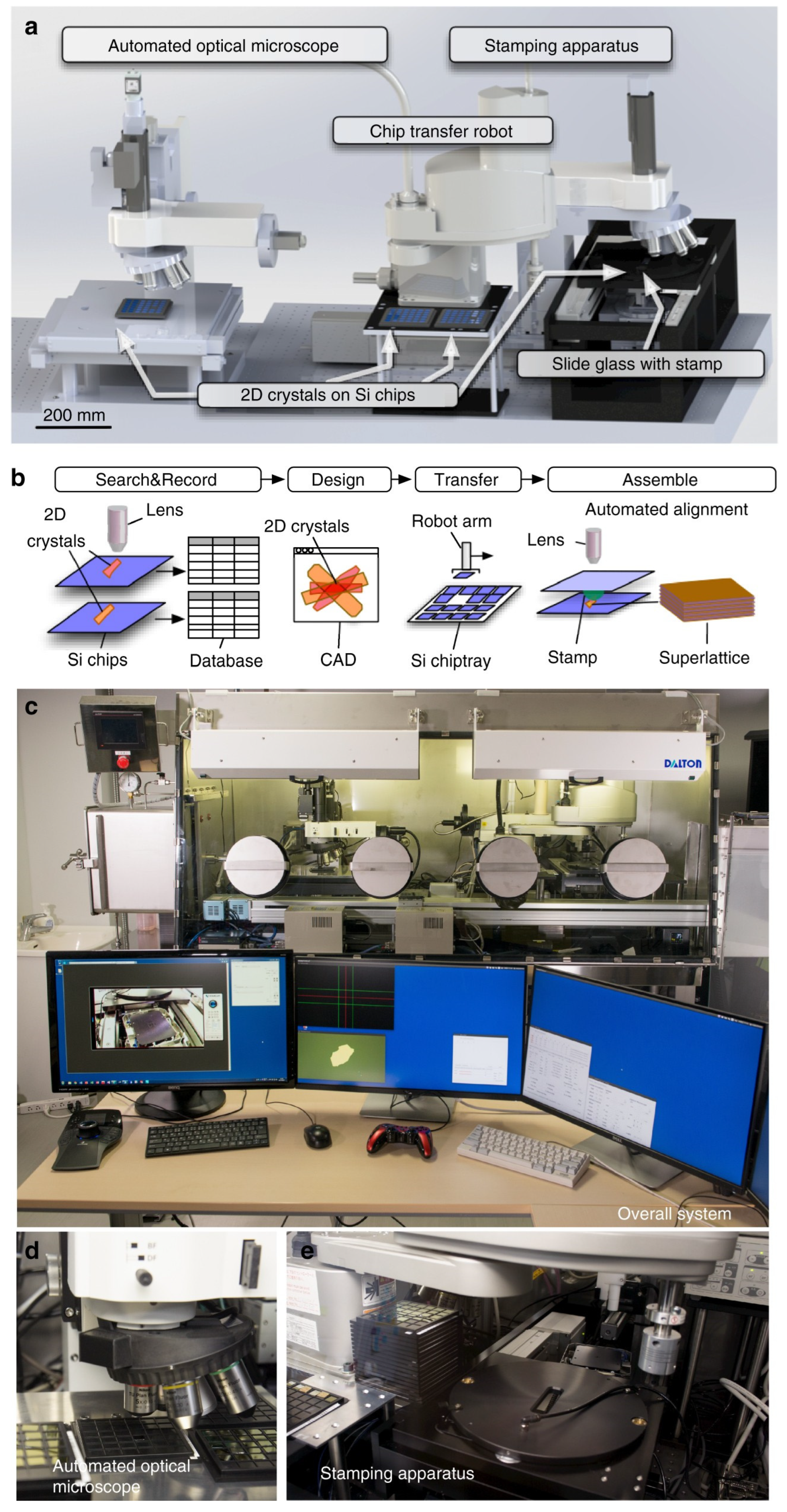
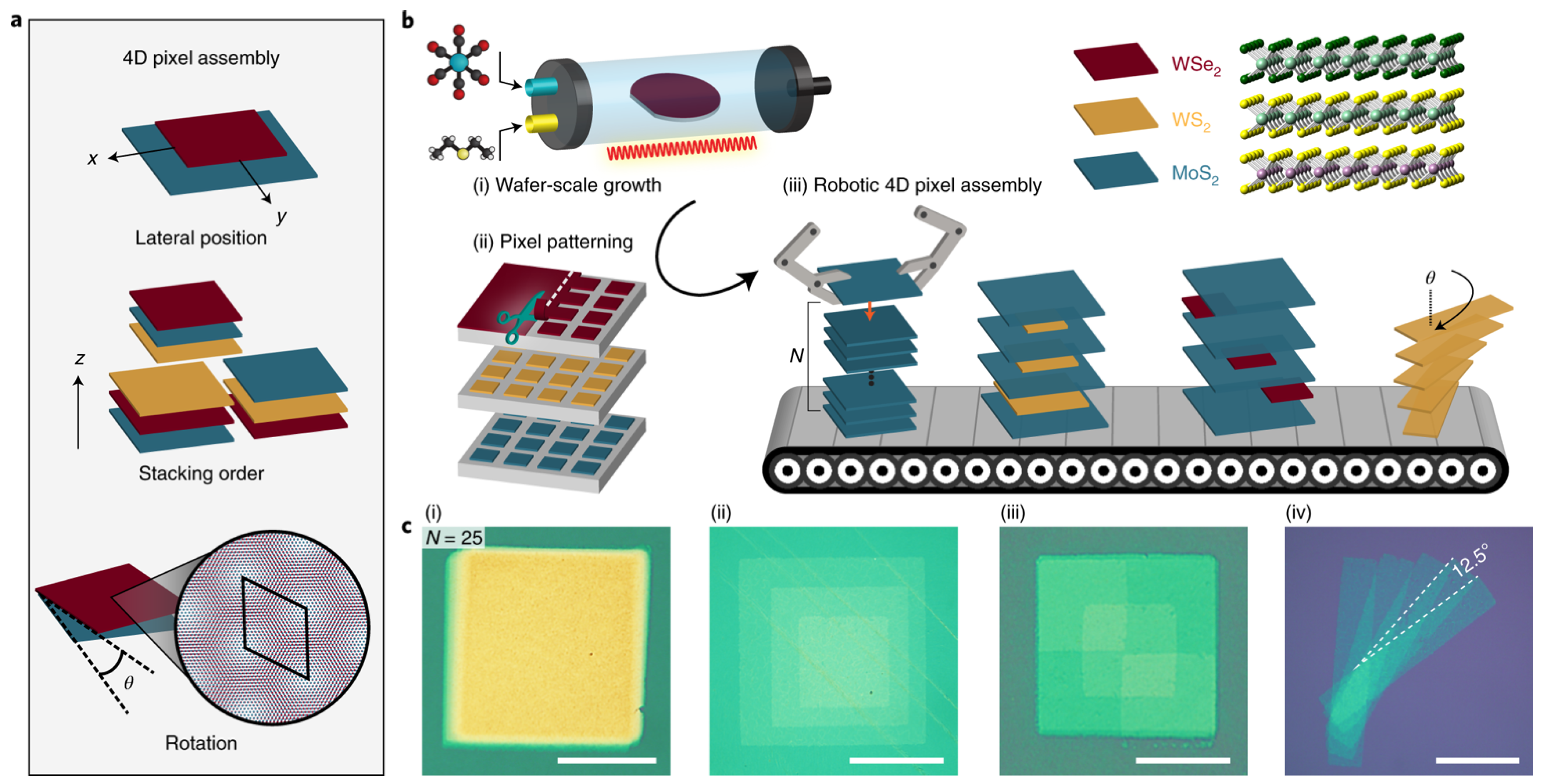
5.2. Setups with Robotic Automation

The study by Masubuchi and colleagues [85] details the development of an autonomous robotic system for the efficient fabrication of van der Waals (vdW) superlattices from two-dimensional (2D) crystals. This system addresses the challenges posed by the manual processes traditionally used for locating and assembling 2D materials. The robotic system (Figure 10) operates within a glovebox to maintain an inert atmosphere. It autonomously detects up to 400 monolayer graphene flakes per hour with a minimal error rate and assembles up to four cycles of 2D crystal stacks per hour, requiring only minimal human intervention. The innovative image processing pipeline and computer-vision algorithms enable the system to distinguish 2D crystals from contaminants accurately. The design of the system includes an automated optical microscope and a stamping apparatus, which together facilitate the high-precision assembly of vdW heterostructures. This technology significantly reduces the time and labor involved in fabricating complex heterostructures, exemplified by the successful construction of a 29-layer graphene and hexagonal boron nitride superlattice. This scalable approach opens new possibilities for prototyping a wide variety of vdW superlattices, advancing both fundamental research and practical applications in nanomaterial science.
In their groundbreaking work published in Nature Nanotechnology, Mannix et al. [88] present a revolutionary method for the high-throughput, precise assembly of van der Waals (vdW) solids using a robotic four-dimensional (4D) pixel assembly technique. This innovative approach overcomes the limitations of traditional micromechanical exfoliation methods, which are not scalable for rapid manufacturing. The team developed a robotic system (Figure 11) capable of assembling prepatterned pixels of atomically thin two-dimensional materials into vdW solids with unprecedented speed, precision, and scale. The method involves wafer-scale growth of two-dimensional material films, clean contact-free patterning, and robotic assembly under high vacuum, enabling the fabrication of vdW solids with up to 80 individual layers and controlled interlayer angles. This technology facilitates efficient optical spectroscopic assays, revealing new excitonic and absorbance layer dependencies in materials such as MoS2. Additionally, the assembly of twisted multilayer structures, like a four-layer WS2 with precise interlayer rotations, demonstrated atomic reconstruction at high twist angles. This robotic 4D pixel assembly method represents a significant advancement in the scalable manufacturing of designer quantum materials, potentially unlocking new possibilities in advanced electronic technologies and the exploration of novel physical phenomena.
The Vacuum Assembly Robot (VAR), as depicted in Figure 12, is a critical component of the four-dimensional pixel assembly process [88]. The VAR is housed in a desktop-size high-vacuum chamber to minimize surface contamination and prevent material oxidation during the assembly of vdW heterostructures. It features a heated x-y translation stage that holds multiple chips of source material or receiving substrates, and a separate z-θ actuated stacking platform for precise layer manipulation. The assembly process involves a micro-structured polymer stamp designed for optimal mechanical properties and thermally switched adhesion. This stamp picks up and deposits layers with high spatial and angular resolution, ensuring accurate layer-by-layer construction. The VAR operates with high efficiency, achieving assembly rates of up to 30 layers per hour. This robotic system allows for fully automated, operator-free fabrication of complex vdW solids, significantly improving throughput and consistency compared to traditional manual or semi-automated methods. The versatility of the VAR makes it applicable to various two-dimensional materials, including transition metal dichalcogenides, gold thin films, and exfoliated flakes, enhancing its potential for widespread use in advanced material manufacturing.
Table 1 summarizes the transfer setups discussed so far, highlighting the transfer methods employed, the corresponding vdW heterostructures formed, and the advantages and limitations of each setup.

6. Outlook and Future Directions

In recent years, the advancement of 2D material fabrication has opened new possibilities for creating high-performance electronic devices. One significant challenge in the deterministic assembly of van der Waals heterostructures through mechanical stacking is the reduction of residues trapped between the stacked layers. These residues often form bubbles and ripples, which limit the effective clean surface area available for final device fabrication [110,111]. As highlighted by Gomez et al. [9], eliminating residues is particularly important for thinner devices, like single and bilayer field-effect transistors (FETs). Such thin devices experience drastic deterioration in electronic properties, including carrier mobility and homogeneity, due to environmental factors, like residual water and oxygen in the transfer chamber. Standard glovebox chambers, which only achieve partial oxygen and water pressures down to 10−4 mbar, fail to provide a sufficiently clean environment, leading to surface damage and inefficient self-cleaning processes in thin crystals. This results in rough interface morphology and complex local strain, contributing to poor device performance. Furthermore, the use of argon or nitrogen environments, even with high-quality gas purification systems, does not completely eliminate hydrocarbon contamination or bubble formation, further degrading the quality of van der Waals interfaces.
As highlighted in Section 5.1 of this review, despite experimental demonstrations showing the potential for fabricating heterostructures under high vacuum, these methods are not yet widely adopted due to their complexity, cost, and scalability issues. Additionally, the transfer method might still involve exposing the 2D materials to air at certain stages of the assembly process [5,88]. Developing cleaner transfer methods or implementing these techniques in controlled ultra-high vacuum environments will be crucial research directions in the near future. A recent review by Dong et al. [78] provides an overview of recent efforts to develop clean 2D materials and devices.
The second challenge is the inherent sample-to-sample variability in manual transfer processes, which are highly dependent on operator skills. This variability complicates not only the comparison of samples produced in different laboratories but also those made in the same laboratory by different researchers or at different times. To address this, the development of robotic approaches [85] using computer vision and machine learning algorithms to autonomously identify, pick up, and transfer materials is an urgent future avenue to be pursued. This is particularly important for research focused on complex heterostructure architectures. With such advancements, van der Waals heterostructures could offer extensive flexibility in the damage-free integration of distinct materials, surpassing the limitations of traditional chemical integration.
Lastly, it is important to develop new experimental setups and techniques for using 2D materials to fabricate more complex systems with enhanced reliability and functionality. Recently, unique and modified techniques have been developed for the deterministic transfer of 2D materials, such as the pick-and-place approach [85], the polyvinyl alcohol (PVA) method [92], viscoelastic stamping [96], Evalcite method [121], the wedging method [125], patterned pick-and-place stamping method [126], patterned monolayer transfer [127], and metal-assisted transfer [128]. Each of these methods helps transfer 2D materials efficiently but is limited by its shortcomings and scope of implementation, such as obtaining a high yield of quality flakes, avoiding cross-contamination of the entire substrate from undesired flake transfer, demonstrating repeatability in device performance, and avoiding undesired residues on flakes [89].
In the context of developing more effective transfer setups, solving the spatial cross-contamination problem of unwanted 2D material crystal flakes on the transfer substrate and yielding good quality flakes is of particular interest. This is a parasitic effect that is often caused by other transfer methods, and eliminating this enables chip-industry-like repeatability [90]. In recent work, Patil et al. [90], introduced a unique two-dimensional material transfer system (2DMTS) designed to address the persistent challenges in 2D material transfer processes. This innovative system, shown in Figure 13, leverages a viscoelastic polymer combined with a metal micro-transfer stamper, enabling exceptional precision and reliability in transferring 2D materials. The micro-stamper offers several key advantages: it allows for selective transfer by ensuring that only the desired material flake is picked up and placed, thereby eliminating cross-contamination. This precision is crucial in applications requiring high purity and accuracy, such as in the fabrication of optoelectronic devices. The high spatial accuracy of the reported system, up to 0.7 µm, is the highest reported to date without cross-contamination. Additionally, the micro-stamper design facilitates the transfer of flakes of varying sizes and shapes without causing damage, thanks to the controlled and gentle contact pressure. This method also enables rapid prototyping without involving wet chemical processes or thermal steps, preserving the intrinsic properties of the 2D materials. By overcoming the limitations of previous methods, the 2DMTS system significantly enhances the efficiency and yield of 2D material transfers, making it a vital tool for advancing research and commercial applications in photonics, electronics, and beyond.
The potential in developing modified micro-manipulator setups is further highlighted in a more recent work [91], where the authors have created a transfer system for the cryogenic dry exfoliation, pick-up, and transfer of superconducting vdW heterostructures such as BSCCO, CrI3, and NbSe2. These materials are known for their chemical sensitivity, which leads to rapid degradation. For instance, BSCCO quickly deteriorates due to the adsorption of water molecules [129,130]. Consequently, fabricating heterostructures involving BSCCO using standard PPC/PC and PDMS stamp methods has faced limitations in controlling these conditions, making the fabrication of twisted BSCCO devices particularly challenging [131].
The developed setup (Figure 14) features a low-temperature stage with a copper surface connected to a liquid nitrogen circulation system via PTFE tubes, allowing precise cryogenic control of the sample. The cryogenic exfoliation technique employs a hemispherical PDMS stamp, enabling the re-exfoliation of thicker BSCCO flakes that were initially mechanically exfoliated on a SiO2/Si chip using scotch tape. The re-exfoliated flake is then immediately transferred onto the remaining flake on the substrate to form the twisted BSCCO junction at −120 °C. This method leverages the glass transition of PDMS for clean cleaving and stacking, avoiding external mechanical force and PDMS residues common in conventional dry transfer methods. The effectiveness of this method in preserving the interfacial and superconducting properties of BSCCO crystals was demonstrated through transport measurements. Additionally, the versatility of the setup was shown by successfully forming twisted CrI3 and NbSe2 heterostructures.
However, this method also presents drawbacks, including the complexity and cost of maintaining cryogenic conditions and the potential for nitrogen condensation, which can affect transfer quality. Moreover, attempts to re-exfoliate other common 2D materials, such as MoS2, WSe2, and GeBi2Te4, were unsuccessful. Despite these challenges, the setup marks a significant step forward in the reliable fabrication and study of vdW heterostructures.
In conclusion, we foresee that integrating innovative approaches discussed above, with robotic automation and “cleanroom in a glovebox” setups, or even low-cost glovebox setups specifically designed for vdW heterostructure stacking, holds significant promise for the future advancement of vdW devices. This approach could greatly enhance the precision, reliability, and scalability of 2D material-based device manufacturing, paving the way for groundbreaking developments across various technological fields.

Funding

This project was funded by the National Research Council of Thailand (NRCT), contract number N42A650226. The Research by King Mongkut’s Institute of Technology Ladkrabang (KMITL) received funding support from the NSRF (FRB660065/0258-RE-KRIS/FF66/14 and FRB660065/0258-RE-KRIS/FF66/13). This research has received funding support from the NSRF via the Program Management Unit for Human Resources and Institutional Development, Research and Innovation (Grant No. B05F640228). H.R. acknowledges support from King Mongkut’s Institute of Technology Ladkrabang (grant no KREF046302).

Conflicts of Interest

The authors declare no conflicts of interest.

References

  1. Geim, A.K.; Grigorieva, I.V. Van der Waals heterostructures. Nature 2013, 499, 419–425. [Google Scholar] [CrossRef] [PubMed]
  2. Liu, Y.; Weiss, N.O.; Duan, X.; Cheng, H.-C.; Huang, Y.; Duan, X. Van der Waals heterostructures and devices. Nat. Rev. Mater. 2016, 1, 16042. [Google Scholar] [CrossRef]
  3. Novoselov, K.S.; Mishchenko, A.; Carvalho, A.; Castro Neto, A.H. 2D materials and van der Waals heterostructures. Science 2016, 353, aac9439. [Google Scholar] [CrossRef] [PubMed]
  4. Jariwala, D.; Marks, T.J.; Hersam, M.C. Mixed-dimensional van der Waals heterostructures. Nat. Mater. 2017, 16, 170–181. [Google Scholar] [CrossRef] [PubMed]
  5. Kang, K.; Lee, K.-H.; Han, Y.; Gao, H.; Xie, S.; Muller, D.A.; Park, J. Layer-by-layer assembly of two-dimensional materials into wafer-scale heterostructures. Nature 2017, 550, 229–233. [Google Scholar] [CrossRef] [PubMed]
  6. Frisenda, R.; Navarro-Moratalla, E.; Gant, P.; De Lara, D.P.; Jarillo-Herrero, P.; Gorbachev, R.V.; Castellanos-Gomez, A. Recent progress in the assembly of nanodevices and van der Waals heterostructures by deterministic placement of 2D materials. Chem. Soc. Rev. 2018, 47, 53–68. [Google Scholar] [CrossRef] [PubMed]
  7. Yankowitz, M.; Ma, Q.; Jarillo-Herrero, P.; LeRoy, B.J. Van der Waals heterostructures combining graphene and hexagonal boron nitride. Nat. Rev. Phys. 2019, 1, 112–125. [Google Scholar] [CrossRef]
  8. Liang, S.J.; Cheng, B.; Cui, X.; Miao, F. Van der Waals heterostructures for high-performance device applications: Challenges and opportunities. Adv. Mater. 2020, 32, 1903800. [Google Scholar] [CrossRef]
  9. Castellanos-Gomez, A.; Duan, X.; Fei, Z.; Gutierrez, H.R.; Huang, Y.; Huang, X.; Quereda, J.; Qian, Q.; Sutter, E.; Sutter, P. Van der Waals heterostructures. Nat. Rev. Methods Primers 2022, 2, 58. [Google Scholar] [CrossRef]
  10. Joo, M.K.; Moon, B.H.; Ji, H.; Han, G.H.; Kim, H.; Lee, G.; Lim, S.C.; Suh, D.; Lee, Y.H. Electron excess doping and effective Schottky barrier reduction on the MoS2/h-BN heterostructure. Nano Lett. 2016, 16, 6383–6389. [Google Scholar] [CrossRef]
  11. Vu, Q.A.; Lee, J.H.; Nguyen, V.L.; Shin, Y.S.; Lim, S.C.; Lee, K.; Heo, J.; Park, S.; Kim, K.; Lee, Y.H.; et al. Tuning carrier tunneling in van der Waals heterostructures for ultrahigh detectivity. Nano Lett. 2017, 17, 453–459. [Google Scholar] [CrossRef] [PubMed]
  12. Vu, Q.A.; Shin, Y.S.; Kim, Y.R.; Nguyen, V.L.; Kang, W.T.; Kim, H.; Luong, D.H.; Lee, I.M.; Lee, K.; Ko, D.S.; et al. Two-terminal floating-gate memory with van der Waals heterostructures for ultrahigh on/off ratio. Nat. Commun. 2016, 7, 12725. [Google Scholar] [CrossRef] [PubMed]
  13. Lee, C.-H.; Lee, G.-H.; van der Zande, A.M.; Chen, W.; Li, Y.; Han, M.; Cui, X.; Arefe, G.; Nuckolls, C.; Heinz, T.F.; et al. Atomically thin p-n junctions with van der Waals heterointerfaces. Nat. Nanotechnol. 2014, 9, 676–681. [Google Scholar] [CrossRef] [PubMed]
  14. Fang, H.; Battaglia, C.; Carraro, C.; Nemsak, S.; Ozdol, B.; Kang, J.S.; Bechtel, H.A.; Desai, S.B.; Kronast, F.; Unal, A.A.; et al. Strong interlayer coupling in van der Waals heterostructures built from single-layer chalcogenides. Proc. Natl. Acad. Sci. USA 2014, 111, 6198–6202. [Google Scholar] [CrossRef] [PubMed]
  15. Hong, X.; Kim, J.; Shi, S.F.; Zhang, Y.; Jin, C.; Sun, Y.; Tongay, S.; Wu, J.; Zhang, Y.; Wang, F. Ultrafast charge transfer in atomically thin MoS2/WS2 heterostructures. Nat. Nanotechnol. 2014, 9, 682–686. [Google Scholar] [CrossRef]
  16. Cheng, R.; Li, D.; Zhou, H.; Wang, C.; Yin, A.; Jiang, S.; Liu, Y.; Chen, Y.; Huang, Y.; Duan, X. Electroluminescence and photocurrent generation from atomically sharp WSe2/MoS2 heterojunction p–n diodes. Nano Lett. 2014, 14, 5590–5597. [Google Scholar] [CrossRef]
  17. Liu, Y.; Huang, Y.; Duan, X. Van der Waals integration before and beyond two-dimensional materials. Nature 2019, 567, 323–333. [Google Scholar] [CrossRef]
  18. Gong, Y.; Lin, J.; Wang, X.; Shi, G.; Lei, S.; Lin, Z.; Zou, X.; Ye, G.; Vajtai, R.; Yakobson, B.I.; et al. Vertical and in-plane heterostructures from WS2/MoS2 monolayers. Nat. Mater. 2014, 13, 1135–1142. [Google Scholar] [CrossRef]
  19. Britnell, L.; Gorbachev, R.V.; Jalil, R.; Belle, B.D.; Schedin, F.; Mishchenko, A.; Georgiou, T.; Katsnelson, M.I.; Eaves, L.; Morozov, S.V.; et al. Field-effect tunneling transistor based on vertical graphene heterostructures. Science 2012, 335, 947–950. [Google Scholar] [CrossRef]
  20. Britnell, L.; Gorbachev, R.V.; Geim, A.K.; Ponomarenko, L.A.; Mishchenko, A.; Greenaway, M.T.; Fromhold, T.M.; Novoselov, K.S.; Eaves, L. Resonant tunnelling and negative differential conductance in graphene transistors. Nat. Commun. 2013, 4, 1794. [Google Scholar] [CrossRef]
  21. Georgiou, T.; Jalil, R.; Belle, B.D.; Britnell, L.; Gorbachev, R.V.; Morozov, S.V.; Kim, Y.J.; Gholinia, A.; Haigh, S.J.; Makarovsky, O.; et al. Vertical field-effect transistor based on graphene–WS2 heterostructures for flexible and transparent electronics. Nat. Nanotechnol. 2013, 8, 100–103. [Google Scholar] [CrossRef] [PubMed]
  22. Yan, R.; Fathipour, S.; Han, Y.; Song, B.; Xiao, S.; Li, M.; Ma, N.; Protasenko, V.; Muller, D.A.; Jena, D.; et al. Esaki diodes in van der Waals heterojunctions with broken-gap energy band alignment. Nano Lett. 2015, 15, 5791–5798. [Google Scholar] [CrossRef] [PubMed]
  23. Yan X, Liu C S, Li C, Bao W Z, Ding S J, Zhang D W and Zhou P 2017 Tunable SnSe2/WSe2 heterostructure tunneling field effect transistor. Small 2017, 13, 1701478.
  24. Jung, Y.; Choi, M.S.; Nipane, A.; Borah, A.; Kim, B.; Zangiabadi, A.; Taniguchi, T.; Watanabe, K.; Yoo, W.J.; Hone, J.; et al. Transferred via contacts as a platform for ideal two-dimensional transistors. Nat. Electron. 2019, 2, 187–194. [Google Scholar] [CrossRef]
  25. Liu, Y.; Guo, J.; Zhu, E.B.; Liao, L.; Lee, S.J.; Ding, M.N.; Shakir, I.; Gambin, V.; Huang, Y.; Duan, X.F. Approaching the Schottky-Mott limit in van der Waals metal-semiconductor junctions. Nature 2018, 557, 696–700. [Google Scholar] [CrossRef] [PubMed]
  26. Chuang, H.J.; Tan, X.B.; Ghimire, N.J.; Perera, M.M.; Chamlagain, B.; Cheng MM, C.; Yan, J.Q.; Mandrus, D.; Tománek, D.; Zhou, Z.X. High mobility WSe2 pand n-type field-effect transistors contacted by highly doped graphene for low-resistance contacts. Nano Lett. 2014, 14, 3594–3601. [Google Scholar] [CrossRef] [PubMed]
  27. Liu, Y.; Wu, H.; Cheng, H.-C.; Yang, S.; Zhu, E.; He, Q.; Ding, M.; Li, D.; Guo, J.; Weiss, N.O.; et al. Toward barrier free contact to molybdenum disulfide using graphene electrodes. Nano Lett. 2015, 15, 3030–3034. [Google Scholar] [CrossRef]
  28. Lee, G.H.; Cui, X.; Kim, Y.D.; Arefe, G.; Zhang, X.; Lee, C.H.; Ye, F.; Watanabe, K.; Taniguchi, T.; Kim, P.; et al. Highly stable, dual-gated MoS2 transistors encapsulated by hexagonal boron nitride with gate-controllable contact, resistance, and threshold voltage. ACS Nano 2015, 9, 7019–7026. [Google Scholar] [CrossRef]
  29. Zhao, B.; Dang, W.; Yang, X.; Li, J.; Bao, H.; Wang, K.; Luo, J.; Zhang, Z.; Li, B.; Xie, H.; et al. Van der Waals epitaxial growth of ultrathin metallic NiSe nanosheets on WSe2 as high-performance contacts for WSe2 transistors. Nano Res. 2019, 12, 1683–1689. [Google Scholar] [CrossRef]
  30. Chen, Y.; Wang, Y.; Wang, Z.; Gu, Y.; Ye, Y.; Chai, X.; Ye, J.; Chen, Y.; Xie, R.; Zhou, Y.; et al. Unipolar barrier photodetectors based on van der Waals heterostructures. Nat. Electron. 2021, 4, 357–363. [Google Scholar] [CrossRef]
  31. Geum, D.-M.; Kim, S.; Khym, J.H.; Lim, J.H.; Kim, S.K.; Ahn, S.-Y.; Kim, T.S.; Kang, K.; Kim, S.H. Arrayed MoS2–In0.53Ga0.47As van der Waals Heterostructure for High-Speed and Broadband Detection from Visible to Shortwave-Infrared Light. Small 2021, 17, 2007357. [Google Scholar] [CrossRef] [PubMed]
  32. Yu, X.; Li, Y.; Hu, X.; Zhang, D.; Tao, Y.; Liu, Z.; He, Y.; Haque, A.; Liu, Z.; Wu, T.; et al. Narrow bandgap oxide nanoparticles coupled with graphene for high performance mid-infrared photodetection. Nat. Commun. 2018, 9, 4299. [Google Scholar] [CrossRef] [PubMed]
  33. Islam, S.; Mishra, J.K.; Kumar, A.; Chatterjee, D.; Ravishankar, N.; Ghosh, A. Ultra-sensitive graphene–bismuth telluride nano-wire hybrids for infrared detection. Nanoscale 2019, 11, 1579. [Google Scholar] [CrossRef] [PubMed]
  34. Wang, F.; Wang, Z.; Xu, K.; Wang, F.; Wang, Q.; Huang, Y.; Yin, L.; He, J. Tunable GaTe-MoS2 van der Waals p–n Junctions with Novel Optoelectronic Performance. Nano Lett. 2015, 15, 7558. [Google Scholar] [CrossRef] [PubMed]
  35. Wu, H.; Kang, Z.; Zhang, Z.; Zhang, Z.; Si, H.; Liao, Q.; Zhang, S.; Wu, J.; Zhang, X.; Zhang, Y. Interfacial Charge Behavior Modulation in Perovskite Quantum Dot-Monolayer MoS2 0D-2D Mixed-Dimensional van der Waals Heterostructures. Adv. Funct. Mater. 2018, 28, 1802015. [Google Scholar] [CrossRef]
  36. Zhang, Y.; Xu, Y.; Guo, J.; Zhang, X.; Liu, X.; Fu, Y.; Zhang, F.; Ma, C.; Shi, Z.; Cao, R.; et al. Designing of 0D/2D mixed-dimensional van der waals heterojunction over ultrathin g-C3N4 for high-performance flexible self-powered photodetector. Chem. Eng. J. 2021, 420 Pt 1, 129556. [Google Scholar] [CrossRef]
  37. Li, X.; Sun, T.; Zhou, K.; Hong, X.; Tang, X.; Wei, D.; Feng, W.; Shen, J.; Wei, D. High-performance Schottky heterojunction photodetector with directly grown graphene nanowalls as electrodes. Nanotechnology 2020, 31, 315204. [Google Scholar] [CrossRef]
  38. Qiao, H.; Li, Z.; Huang, Z.; Ren, X.; Kang, J.; Qiu, M.; Liu, Y.; Qi, X.; Zhong, J.; Zhang, H. Self-powered photodetectors based on 0D/2D mixed dimensional heterojunction with black phosphorus quantum dots as hole accepters. Appl. Mater. Today 2020, 20, 100765. [Google Scholar] [CrossRef]
  39. Zhang, K.; Fang, X.; Wang, Y.; Wan, Y.; Song, Q.; Zhai, W.; Li, Y.; Ran, G.; Ye, Y.; Dai, L. Ultrasensitive Near-Infrared Photodetectors Based on a Graphene–MoTe2–Graphene Vertical van der Waals Heterostructure. ACS Appl. Mater. Interfaces 2017, 9, 5392–5398. [Google Scholar] [CrossRef]
  40. Wu, D.; Mo, Z.; Han, Y.; Lin, P.; Shi, Z.; Chen, X.; Tian, Y.; Li, X.J.; Yuan, H.; Tsang, Y.H. Fabrication of 2D PdSe2/3D CdTe Mixed-Dimensional van der Waals Heterojunction for Broadband Infrared Detection. ACS Appl. Mater. Interfaces 2021, 13, 41791–41801. [Google Scholar] [CrossRef]
  41. Liu, L.X.; Zhai, T.Y. Wafer-scale vertical van der Waals heterostructures. InfoMat 2021, 3, 3–21. [Google Scholar] [CrossRef]
  42. Long, M.; Wang, Y.; Wang, P.; Zhou, X.; Xia, H.; Luo, C.; Huang, S.; Zhang, G.; Yan, H.; Fan, Z.; et al. Palladium diselenide long-wavelength infrared photodetector with high sensitivity and stability. ACS Nano 2019, 13, 2511–2519. [Google Scholar] [CrossRef] [PubMed]
  43. Bullock, J.; Amani, M.; Cho, J.; Chen, Y.-Z.; Ahn, G.H.; Adinolfi, V.; Shrestha, V.R.; Gao, Y.; Crozier, K.B.; Chueh, Y.-L. Polarization-resolved black phosphorus/molybdenum disulfide mid-wave infrared photodiodes with high detectivity at room temperature. Nat. Photon. 2018, 12, 601–607. [Google Scholar] [CrossRef]
  44. Long, M.; Liu, E.; Wang, P.; Gao, A.; Xia, H.; Luo, W.; Wang, B.; Zeng, J.; Fu, Y.; Xu, K.; et al. Broadband photovoltaic detectors based on an atomically thin heterostructure. Nano Lett. 2016, 16, 2254–2259. [Google Scholar] [CrossRef] [PubMed]
  45. Gao, A.; Lai, J.; Wang, Y.; Zhu, Z.; Zeng, J.; Yu, G.; Wang, N.; Chen, W.; Cao, T.; Hu, W.; et al. Observation of ballistic avalanche phenomena in nanoscale vertical InSe/BP heterostructures. Nat. Nanotechnol. 2019, 14, 217–222. [Google Scholar] [CrossRef] [PubMed]
  46. Furchi, M.M.; Höller, F.; Dobusch, L.; Polyushkin, D.K.; Schuler, S. Device physics of van der Waals heterojunction solar cells. NPJ 2D Mater. Appl. 2018, 2, 3. [Google Scholar] [CrossRef]
  47. Cao, J.; Tang, G.; You, P.; Wang, T.; Zheng, F.; Zhao, J.; Yan, F. Enhanced Performance of Planar Perovskite Solar Cells Induced by Van Der Waals Epitaxial Growth of Mixed Perovskite Films on WS2 Flakes. Adv. Funct. Mater. 2020, 30, 2002358. [Google Scholar] [CrossRef]
  48. Cao, F.; Bian, L.; Li, L. Perovskite solar cells with high-efficiency exceeding 25%: A review. Energy Mater. Devices 2024, 2, 9370018. [Google Scholar] [CrossRef]
  49. Sun, X.; Zhang, B.; Li, Y.; Luo, X.; Li, G.; Chen, Y.; Zhang, C.; He, J. Tunable Ultrafast Nonlinear Optical Properties of Graphene/MoS2 van der Waals Heterostructures and Their Application in Solid-State Bulk Lasers. ACS Nano 2018, 12, 11376–11385. [Google Scholar] [CrossRef]
  50. Li, P.; Yuan, K.; Lin, D.-Y.; Wang, T.; Du, W.; Wei, Z.; Watanabe, K.; Taniguchi, T.; Ye, Y.; Dai, L. p-MoS2/n-InSe van der Waals heterojunctions and their applications in all-2D optoelectronic devices. RSC Adv. 2019, 9, 35039–35044. [Google Scholar] [CrossRef]
  51. Zong, X.; Hu, H.; Ouyang, G.; Wang, J.; Shi, R.; Zhang, L.; Zeng, Q.; Zhu, C.; Chen, S.; Cheng, C.; et al. Black phosphorus-based van der Waals heterostructures for mid-infrared light-emission applications. Light-Sci. Appl. 2020, 9, 114. [Google Scholar] [CrossRef] [PubMed]
  52. Hou, L.; Zhang, Q.; Shautsova, V.; Warner, J.H. Operational Limits and Failure Mechanisms in All-2D van der Waals Vertical Heterostructure Devices with Long-Lived Persistent Electroluminescence. ACS Nano 2020, 14, 15533–15543. [Google Scholar] [CrossRef] [PubMed]
  53. Song, S.-B.; Yoon, S.; Kim, S.Y.; Yang, S.; Seo, S.-Y.; Cha, S.; Jeong, H.-W.; Watanabe, K.; Taniguchi, T.; Lee, G.-H.; et al. Deep-ultraviolet electroluminescence and photocurrent generation in graphene/hBN/graphene heterostructures. Nat. Commun. 2021, 12, 7134. [Google Scholar] [CrossRef] [PubMed]
  54. Donarelli, M.; Ottaviano, L. 2D Materials for Gas Sensing Applications: A Review on Graphene Oxide, MoS2, WS2 and Phosphorene. Sensors 2018, 18, 3638. [Google Scholar] [CrossRef] [PubMed]
  55. Liu, X.; Ma, T.; Pinna, N.; Zhang, J. Two-Dimensional Nanostructured Materials for Gas Sensing. Adv. Funct. Mater. 2017, 27, 1702168. [Google Scholar] [CrossRef]
  56. Hou, H.-L.; Anichini, C.; Samorì, P.; Criado, A.; Prato, M. 2D Van der Waals Heterostructures for Chemical Sensing. Adv. Funct. Mater. 2022, 32, 2207065. [Google Scholar] [CrossRef]
  57. Kang, L.; Jiang, P.; Cao, N.; Hao, H.; Zheng, X.; Zhang, L.; Zeng, Z. Realizing giant tunneling electroresistance in two-dimensional graphene/BiP ferroelectric tunnel junction. Nanoscale 2019, 11, 16837–16843. [Google Scholar] [CrossRef] [PubMed]
  58. Shen, X.-W.; Fang, Y.-W.; Tian, B.-B.; Duan, C.-G. Two-Dimensional Ferroelectric Tunnel Junction: The Case of Monolayer In:SnSe/SnSe/Sb:SnSe Homostructure. ACS Appl. Electron. Mater. 2019, 1, 1133. [Google Scholar] [CrossRef]
  59. Sun, L.; Zhang, Y.; Han, G.; Hwang, G.; Jiang, J.; Joo, B.; Watanabe, K.; Taniguchi, T.; Kim, Y.-M.; Yu, W.J.; et al. Self-selective van der Waals heterostructures for large scale memory array. Nat. Commun. 2019, 10, 3161. [Google Scholar] [CrossRef]
  60. Kang, L.; Jiang, P.; Hao, H.; Zhou, Y.; Zheng, X.; Zhang, L.; Zeng, Z. Giant tunneling electroresistance in two-dimensional ferroelectric tunnel junctions with out-of-plane ferroelectric polarization. Phys. Rev. B 2020, 101, 014105. [Google Scholar] [CrossRef]
  61. Zhang, W.; Gao, H.; Deng, C.; Lv, T.; Hu, S.; Wu, H.; Xue, S.; Tao, Y.; Deng, L.; Xiong, W. An ultrathin memristor based on a two-dimensional WS2/MoS2 heterojunction. Nanoscale 2021, 13, 11497–11504. [Google Scholar] [CrossRef] [PubMed]
  62. Wang, X.; Zhu, C.; Deng, Y.; Duan, R.; Chen, J.; Zeng, Q.; Zhou, J.; Fu, Q.; You, L.; Liu, S.; et al. Van der Waals engineering of ferroelectric heterostructures for long-retention memory. Nat. Commun. 2021, 12, 1109. [Google Scholar] [CrossRef] [PubMed]
  63. Mao, J.; Wu, S.; Ding, G.; Wang, Z.; Qian, F.; Yang, J.; Zhou, Y.; Han, S. A van der Waals Integrated Damage-Free Memristor Based on Layered 2D Hexagonal Boron Nitride. Small 2022, 18, 2106253. [Google Scholar] [CrossRef] [PubMed]
  64. Paul, T.; Ahmed, T.; Tiwari, K.K.; Thakur, C.S.; Ghosh, A. A high-performance MoS2 synaptic device with floating gate engineering for neuromorphic computing. 2D Mater. 2019, 6, 045008. [Google Scholar] [CrossRef]
  65. Wang, C.-Y.; Liang, S.-J.; Wang, S.; Wang, P.; Li, Z.; Wang, Z.; Gao, A.; Pan, C.; Liu, C.; Liu, J.; et al. Gate-tunable van der Waals heterostructure for reconfigurable neural network vision sensor. Sci. Adv. 2020, 6, eaba6173. [Google Scholar] [CrossRef] [PubMed]
  66. Zhang, Z.-C.; Li, Y.; Wang, J.-J.; Qi, D.-H.; Yao, B.-W.; Yu, M.-X.; Chen, X.-D.; Lu, T.-B. Synthesis of wafer-scale graphdiyne/graphene heterostructure for scalable neuromorphic computing and artificial visual systems. Nano Res. 2021, 14, 4591–4600. [Google Scholar] [CrossRef]
  67. Hou, Y.-X.; Li, Y.; Zhang, Z.-C.; Li, J.-Q.; Qi, D.-H.; Chen, X.-D.; Wang, J.-J.; Yao, B.-W.; Yu, M.-X.; Lu, T.-B.; et al. Large-Scale and Flexible Optical Synapses for Neuromorphic Computing and Integrated Visible Information Sensing Memory Processing. ACS Nano 2021, 15, 1497–1508. [Google Scholar] [CrossRef] [PubMed]
  68. Xiong, X.; Kang, J.; Hu, Q.; Gu, C.; Gao, T.; Li, X.; Wu, Y. Reconfigurable Logic-in-Memory and Multilingual Artificial Synapses Based on 2D Heterostructures. Adv. Funct. Mater. 2020, 30, 1909645. [Google Scholar] [CrossRef]
  69. Kim, C.; Yoon, M.A.; Jang, B.; Kim, J.H.; Kim, K.S. A review on transfer process of two-dimensional materials. Tribol. Lubr. 2020, 36, 1–10. [Google Scholar]
  70. Fan, S.; Vu, Q.A.; Tran, M.D.; Adhikari, S.; Lee, Y.H. Transfer assembly for two-dimensional van der Waals heterostructures. 2D Mater. 2020, 7, 022005. [Google Scholar] [CrossRef]
  71. Guo, H.W.; Hu, Z.; Liu, Z.B.; Tian, J.G. Stacking of 2D materials. Adv. Funct. Mater. 2021, 31, 2007810. [Google Scholar] [CrossRef]
  72. Hu, Z.; Liu, Z.B.; Tian, J.G. Stacking of exfoliated two-dimensional materials: A review. Chin. J. Chem. 2020, 38, 981–995. [Google Scholar] [CrossRef]
  73. Onodera, M.; Masubuchi, S.; Moriya, R.; Machida, T. Assembly of van der Waals heterostructures: Exfoliation, searching, and stacking of 2D materials. Jpn. J. Appl. Phys. 2020, 59, 010101. [Google Scholar] [CrossRef]
  74. Schranghamer, T.F.; Sharma, M.; Singh, R.; Das, S. Review and comparison of layer transfer methods for two-dimensional materials for emerging applications. Chem. Soc. Rev. 2021, 50, 11032–11054. [Google Scholar] [CrossRef] [PubMed]
  75. Watson, A.J.; Lu, W.; Guimarães, M.H.; Stöhr, M. Transfer of large-scale two-dimensional semiconductors: Challenges and developments. 2D Mater. 2021, 8, 032001. [Google Scholar] [CrossRef]
  76. Babar, Z.U.D.; Raza, A.; Cassinese, A.; Iannotti, V. Two Dimensional Heterostructures for Optoelectronics: Current Status and Future Perspective. Molecules 2023, 28, 2275. [Google Scholar] [CrossRef] [PubMed]
  77. Kim, J.Y.; Ju, X.; Ang, K.W.; Chi, D. Van der Waals layer transfer of 2D materials for monolithic 3D electronic system integration: Review and outlook. ACS Nano 2023, 17, 1831–1844. [Google Scholar] [CrossRef]
  78. Dong, W.; Dai, Z.; Liu, L.; Zhang, Z. Toward Clean 2D Materials and Devices: Recent Progress in Transfer and Cleaning Methods. Adv. Mater. 2023, 36, e2303014. [Google Scholar] [CrossRef]
  79. Fan, S.; Li, X.; Mondal, A.; Wang, W.; Lee, Y.H. Strategy for transferring van der Waals materials and heterostructures. 2D Mater. 2024, 11, 033002. [Google Scholar] [CrossRef]
  80. Cheliotis, I.; Zergioti, I. A review on transfer methods of two-dimensional materials. 2D Mater. 2024, 11, 022004. [Google Scholar] [CrossRef]
  81. Zhao, Q.; Wang, T.; Ryu, Y.K.; Frisenda, R.; Castellanos-Gomez, A. An inexpensive system for the deterministic transfer of 2D materials. J. Phys. Mater. 2020, 3, 016001. [Google Scholar] [CrossRef]
  82. Gant, P.; Carrascoso, F.; Zhao, Q.; Ryu, Y.; Seitz, M.; Prins, F.; Frisenda, R.; Castellanos-Gomez, A. A system for the deterministic transfer of 2D materials under inert environmental conditions. 2D Mater. 2020, 7, 025034. [Google Scholar] [CrossRef]
  83. Buapan, K.; Somphonsane, R.; Chiawchan, T.; Ramamoorthy, H. Versatile, low-cost, and portable 2D material transfer setup with a facile and highly efficient DIY inert-atmosphere glove compartment option. ACS Omega 2021, 6, 17952–17964. [Google Scholar] [CrossRef]
  84. Chae, S.H.; Jin, Y.; Kim, T.S.; Chung, D.S.; Na, H.; Nam, H.; Kim, H.; Perello, D.J.; Jeong, H.Y.; Ly, T.H.; et al. Oxidation effect in octahedral hafnium disulfide thin film. ACS Nano 2016, 10, 1309–1316. [Google Scholar] [CrossRef] [PubMed]
  85. Masubuchi, S.; Morimoto, M.; Morikawa, S.; Onodera, M.; Asakawa, Y.; Watanabe, K.; Taniguchi, T.; Machida, T. Autonomous robotic searching and assembly of two-dimensional crystals to build van der Waals superlattices. Nat. Commun. 2018, 9, 1413. [Google Scholar] [CrossRef]
  86. Gray, M.J.; Kumar, N.; O’Connor, R.; Hoek, M.; Sheridan, E.; Doyle, M.C.; Romanelli, M.L.; Osterhoudt, G.B.; Wang, Y.; Plisson, V.; et al. A cleanroom in a glovebox. Rev. Sci. Instrum. 2020, 91, 073909. [Google Scholar] [CrossRef] [PubMed]
  87. Duleba, A.; Pugachev, M.; Blumenau, M.; Martanov, S.; Naumov, M.; Shupletsov, A.; Kuntsevich, A. Inert-Atmosphere Microfabrication Technology for 2D Materials and Heterostructures. Micromachines 2023, 15, 94. [Google Scholar] [CrossRef]
  88. Mannix, A.J.; Ye, A.; Sung, S.H.; Ray, A.; Mujid, F.; Park, C.; Lee, M.; Kang, J.H.; Shreiner, R.; High, A.A.; et al. Robotic four-dimensional pixel assembly of van der Waals solids. Nat. Nanotechnol. 2022, 17, 361–366. [Google Scholar] [CrossRef]
  89. Hemnani, R.A.; Tischler, J.P.; Carfano, C.; Maiti, R.; Tahersima, M.H.; Bartels, L.; Agarwal, R.; Sorger, V.J. 2D material printer: A deterministic cross contamination-free transfer method for atomically layered materials. 2D Mater. 2018, 6, 015006. [Google Scholar] [CrossRef]
  90. Patil, C.; Dalir, H.; Kang, J.H.; Davydov, A.; Wong, C.W.; Sorger, V.J. Highly accurate, reliable, and non-contaminating two-dimensional material transfer system. Appl. Phys. Rev. 2022, 9, 011419. [Google Scholar] [CrossRef]
  91. Patil, V.; Ghosh, S.; Basu, A.; Kuldeep; Dutta, A.; Agrawal, K.; Bhatia, N.; Shah, A.; Jangade, D.A.; Kulkarni, R.; et al. Pick-up and assembling of chemically sensitive van der Waals heterostructures using dry cryogenic exfoliation. Sci. Rep. 2024, 14, 11097. [Google Scholar] [CrossRef]
  92. Dean, C.R.; Young, A.F.; Meric, I.; Lee, C.; Wang, L.; Sorgenfrei, S.; Watanabe, K.; Taniguchi, T.; Kim, P.; Shepard, K.L.; et al. Boron nitride substrates for high-quality graphene electronics. Nat. Nanotechnol. 2010, 5, 722–726. [Google Scholar] [CrossRef]
  93. Kwon, K.C.; Choi, S.; Hong, K.; Moon, C.; Shim, Y.-S.; Kim, D.H.; Kim, T.L.; Sohn, W.; Jeon, J.-M.; Lee, C.-H.; et al. Wafer-scale transferable molybdenum disulfide thin-film catalysts for photoelectrochemical hydrogen production. Energy Environ. Sci. 2016, 9, 2240–2248. [Google Scholar] [CrossRef]
  94. Yuan, J.; Sun, T.; Hu, Z.; Yu, W.; Ma, W.; Zhang, K.; Sun, B.; Lau, S.P.; Bao, Q.; Lin, S.; et al. Wafer-scale fabrication of two-dimensional PtS2/PtSe2 heterojunctions for efficient and broad band photodetection. ACS Appl. Mater. Interfaces 2018, 10, 40614–40622. [Google Scholar] [CrossRef] [PubMed]
  95. Han, S.S.; Ko, T.J.; Yoo, C.; Shawkat, M.S.; Li, H.; Kim, B.K.; Hong, W.K.; Bae, T.S.; Chung, H.S.; Oh, K.H.; et al. Automated assembly of wafer-scale 2D TMD heterostructures of arbitrary layer orientation and stacking sequence using water dissoluble salt substrates. Nano Lett. 2020, 20, 3925–3934. [Google Scholar] [CrossRef]
  96. Castellanos-Gomez, A.; Buscema, M.; Molenaar, R.; Singh, V.; Janssen, L.; Van Der Zant, H.S.; Steele, G.A. Deterministic transfer of two-dimensional materials by all-dry viscoelastic stamping. 2D Mater. 2014, 1, 011002. [Google Scholar] [CrossRef]
  97. Wang, L.; Meric, I.; Huang, P.Y.; Gao, Q.; Gao, Y.; Tran, H.; Taniguchi, T.; Watanabe, K.; Campos, L.M.; Muller, D.A.; et al. One-dimensional electrical contact to a two-dimensional material. Science 2013, 342, 614–617. [Google Scholar] [CrossRef] [PubMed]
  98. Tao, Q.; Wu, R.; Li, Q.; Kong, L.; Chen, Y.; Jiang, J.; Lu, Z.; Li, B.; Li, W.; Li, Z.; et al. Reconfigurable electronics by disassembling and reassembling van der Waals heterostructures. Nat. Commun. 2021, 12, 1825. [Google Scholar] [CrossRef]
  99. Tao, L.; Li, H.; Gao, Y.; Chen, Z.; Wang, L.; Deng, Y.; Zhang, J.; Xu, J.-B. Deterministic and Etching-Free Transfer of Large-Scale 2D Layered Materials for Constructing Interlayer Coupled van der Waals Heterostructures. Adv. Mater. Technol. 2018, 3, 1700282. [Google Scholar] [CrossRef]
  100. Debnath, R.; Sett, S.; Biswas, R.; Raghunathan, V.; Ghosh, A. A simple fabrication strategy for orientationally accurate twisted heterostructures. Nanotechnology 2021, 32, 455705. [Google Scholar] [CrossRef]
  101. Kinoshita, K.; Moriya, R.; Onodera, M.; Wakafuji, Y.; Masubuchi, S.; Watanabe, K.; Taniguchi, T.; Machida, T. Dry release transfer of graphene and few-layer h-BN by utilizing thermoplasticity of polypropylene carbonate. NPJ 2D Mater. Appl. 2019, 3, 22. [Google Scholar] [CrossRef]
  102. Martanov, S.G.; Zhurbina, N.K.; Pugachev, M.V.; Duleba, A.I.; Akmaev, M.A.; Belykh, V.V.; Kuntsevich, A.Y. Making van der Waals heterostructures assembly accessible to everyone. Nanomaterials 2020, 10, 2305. [Google Scholar] [CrossRef] [PubMed]
  103. Kim, K.; Yankowitz, M.; Fallahazad, B.; Kang, S.; Movva, H.C.P.; Huang, S.; Larentis, S.; Corbet, C.M.; Taniguchi, T.; Watanabe, K.; et al. Van der Waals Heterostructures with High Accuracy Rotational Alignment. Nano Lett. 2016, 16, 1989–1995. [Google Scholar] [CrossRef]
  104. Cao, Y.; Fatemi, V.; Fang, S.; Watanabe, K.; Taniguchi, T.; Kaxiras, E.; Jarillo-Herrero, P. Unconventional superconductivity in magic angle graphene superlattices. Nature 2018, 556, 43–50. [Google Scholar] [CrossRef]
  105. Lin, M.-L.; Tan, Q.-H.; Wu, J.-B.; Chen, X.-S.; Wang, J.-H.; Pan, Y.-H.; Zhang, X.; Cong, X.; Zhang, J.; Ji, W.; et al. Moiré Phonons in Twisted Bilayer MoS2. ACS Nano 2018, 12, 8770–8780. [Google Scholar] [CrossRef] [PubMed]
  106. Boddison-Chouinard, J.; Plumadore, R.; Luican-Mayer, A. Fabricating van der Waals Heterostructures with Precise Rotational Alignment. J. Vis. Exp. 2019, 149, e59727. [Google Scholar]
  107. Uwanno, T.; Hattori, Y.; Taniguchi, T.; Watanabe, K.; Nagashio, K. Fully dry PMMA transfer of graphene on h-BN using a heating/cooling system. 2D Mater. 2015, 2, 041002. [Google Scholar] [CrossRef]
  108. Martinez-Duarte, R. Easy and Inexpensive Fabrication of PDMS Films of Different Thicknesses. Chips and Tips (Lab on a Chip). 2012. Available online: https://blogs.rsc.org/chipsandtips/2012/04/18/easy-and-inexpensive-fabrication-of-pdms-films-of-different-thicknesses/ (accessed on 1 June 2024).
  109. Jain, A.; Bharadwaj, P.; Heeg, S.; Parzefall, M.; Taniguchi, T.; Watanabe, K.; Novotny, L. Minimizing residues and strain in 2D materials transferred from PDMS. Nanotechnology 2018, 29, 265203. [Google Scholar] [CrossRef]
  110. Haigh, S.J.; Gholinia, A.; Jalil, R.; Romani, S.; Britnell, L.; Elias, D.C.; Novoselov, K.S.; Ponomarenko, L.A.; Geim, A.K.; Gorbachev, R. Cross-sectional imaging of individual layers and buried interfaces of graphene-based heterostructures and superlattices. Nat. Mater. 2012, 11, 764–767. [Google Scholar] [CrossRef]
  111. Kretinin, A.V.; Cao, Y.; Tu, J.S.; Yu, G.L.; Jalil, R.; Novoselov, K.S.; Haigh, S.J.; Gholinia, A.; Mishchenko, A.; Lozada, M.; et al. Electronic properties of graphene encapsulated with different two-dimensional atomic crystals. Nano Lett. 2014, 14, 3270–3276. [Google Scholar] [CrossRef]
  112. Rooney, A.P.; Kozikov, A.; Rudenko, A.N.; Prestat, E.; Hamer, M.J.; Withers, F.; Cao, Y.; Novoselov, K.S.; Katsnelson, M.I.; Gorbachev, R.; et al. Observing imperfection in atomic interfaces for van der Waals heterostructures. Nano Lett. 2017, 17, 5222–5228. [Google Scholar] [CrossRef] [PubMed]
  113. Cao, Y.; Mishchenko, A.; Yu, G.L.; Khestanova, E.; Rooney, A.P.; Prestat, E.; Kretinin, A.V.; Blake, P.; Shalom, M.B.; Woods, C.; et al. Quality heterostructures from two-dimensional crystals unstable in air by their assembly in inert atmosphere. Nano Lett. 2015, 15, 4914–4921. [Google Scholar] [CrossRef] [PubMed]
  114. Bandurin, D.A.; Tyurnina, A.V.; Yu, G.L.; Mishchenko, A.; Zólyomi, V.; Morozov, S.V.; Kumar, R.K.; Gorbachev, R.V.; Kudrynskyi, Z.R.; Pezzini, S.; et al. High electron mobility, quantum Hall effect and anomalous optical response in atomically thin InSe. Nat. Nanotechnol. 2017, 12, 223–227. [Google Scholar] [CrossRef] [PubMed]
  115. Mishra, R.K.; Sarkar, J.; Chianella, I.; Goel, S.; Nezhad, H.Y. Black phosphorus: The rise of phosphorene in 2D materials applications. Next Mater. 2024, 4, 100217. [Google Scholar] [CrossRef]
  116. Island, J.O.; Steele, G.A.; van der Zant, H.S.; Castellanos-Gomez, A. Environmental instability of few-layer black phosphorus. 2D Mater. 2015, 2, 011002. [Google Scholar] [CrossRef]
  117. Wood, J.D.; Wells, S.A.; Jariwala, D.; Chen, K.S.; Cho, E.; Sangwan, V.K.; Liu, X.; Lauhon, L.J.; Marks, T.J.; Hersam, M.C. Effective passivation of exfoliated black phosphorus transistors against ambient degradation. Nano Lett. 2014, 14, 6964–6970. [Google Scholar] [CrossRef] [PubMed]
  118. Kim, J.S.; Liu, Y.; Zhu, W.; Kim, S.; Wu, D.; Tao, L.; Dodabalapur, A.; Lai, K.; Akinwande, D. Toward air-stable multilayer phosphorene thin-films and transistors. Sci. Rep. 2015, 5, 8989. [Google Scholar] [CrossRef] [PubMed]
  119. Chen, X.; Wu, Y.; Wu, Z.; Han, Y.; Xu, S.; Wang, L.; Ye, W.; Han, T.; He, Y.; Cai, Y.; et al. High-quality sandwiched black phosphorus heterostructure and its quantum oscillations. Nat. Commun. 2015, 6, 7315. [Google Scholar] [CrossRef]
  120. Huang, B.; Clark, G.; Navarro-Moratalla, E.; Klein, D.R.; Cheng, R.; Seyler, K.L.; Zhong, D.; Schmidgall, E.; McGuire, M.A.; Cobden, D.H.; et al. Layer-dependent ferromagnetism in a van der Waals crystal down to the monolayer limit. Nature 2017, 546, 270–273. [Google Scholar] [CrossRef]
  121. Zomer, P.J.; Dash, S.P.; Tombros, N.; Van Wees, B.J. A transfer technique for high mobility graphene devices on commercially available hexagonal boron nitride. Appl. Phys. Lett. 2011, 99, 232104. [Google Scholar] [CrossRef]
  122. Ma, X.; Liu, Q.; Xu, D.; Zhu, Y.; Kim, S.; Cui, Y.; Zhong, L.; Liu, M. Capillary-Force-Assisted Clean-Stamp Transfer of Two-Dimensional Materials. Nano Lett. 2017, 17, 6961–6967. [Google Scholar] [CrossRef] [PubMed]
  123. Zhang, Y.; Liu, Q.; Xu, B. Liquid-Assisted, Etching-Free, Mechanical Peeling of 2D Materials. Extrem. Mech. Lett. 2017, 16, 33–40. [Google Scholar] [CrossRef]
  124. Hou, Y.; Ren, X.; Fan, J.; Wang, G.; Dai, Z.; Jin, C.; Wang, W.; Zhu, Y.; Zhang, S.; Liu, L.; et al. Preparation of Twisted Bilayer Graphene via the Wetting Transfer Method. ACS Appl. Mater. Interfaces 2020, 12, 40958–40967. [Google Scholar] [CrossRef] [PubMed]
  125. Schneider, G.F.; Calado, V.E.; Zandbergen, H.; Vandersypen, L.M.; Dekker, C. Wedging transfer of nanostructures. Nano Lett. 2010, 10, 1912–1916. [Google Scholar] [CrossRef]
  126. Lim, J.Y.; Jang, H.S.; Yoo, H.J.; Kim, S.I.; Whang, D. Pattern pick and place method for twisted Bi-and multi-layer graphene. Materials 2019, 12, 3740. [Google Scholar] [CrossRef]
  127. Gramling, H.M.; Towle, C.M.; Desai, S.B.; Sun, H.; Lewis, E.C.; Nguyen, V.D.; Ager, J.W.; Chrzan, D.; Yeatman, E.M.; Javey, A.; et al. Spatially precise transfer of patterned monolayer WS2 and MoS2 with features larger than 104 μm2 directly from multilayer sources. ACS Appl. Electron. Mater. 2019, 1, 407–416. [Google Scholar] [CrossRef]
  128. Nguyen, V.; Gramling, H.; Towle, C.; Li, W.; Lien, D.H.; Kim, H.; Chrzan, D.C.; Javey, A.; Xu, K.; Ager, J.; et al. Deterministic assembly of arrays of lithographically defined WS2 and MoS2 monolayer features directly from multilayer sources into van der Waals heterostructures. J. Micro-Nano-Manuf. 2019, 7, 041006. [Google Scholar] [CrossRef]
  129. Jiang, D.; Hu, T.; You, L.; Li, Q.; Li, A.; Wang, H.; Mu, G.; Chen, Z.; Zhang, H.; Yu, G.; et al. High-Tc superconductivity in ultrathin Bi2Sr2CaCu2O8+x down to half-unit-cell thickness by protection with graphene. Nat. Commun. 2014, 5, 5708. [Google Scholar] [CrossRef]
  130. Sandilands, L.J.; Shen, J.X.; Chugunov, G.M.; Zhao, S.Y.F.; Ono, S.; Ando, Y.; Burch, K.S. Stability of exfoliated Bi2Sr2DyxCa1–xCu2O8+x studied by Raman microscopy. Phys. Rev. B 2010, 82, 064503. [Google Scholar] [CrossRef]
  131. Lee, Y.; Martini, M.; Confalone, T.; Shokri, S.; Saggau, C.N.; Wolf, D.; Gu, G.; Watanabe, K.; Taniguchi, T.; Montemurro, D.; et al. Encapsulating high-temperature superconducting twisted van der Waals heterostructures blocks detrimental effects of disorder. Adv. Mater. 2023, 35, e2209135. [Google Scholar] [CrossRef]
Figure 2. (a) Schematics and photo of the substrate holder and the electronic box used by Martanov et al. [102] Reprinted from ref. [102] under Creative Common CC by 4.0 license. (b) Photograph showing the details of construction of the substrate heater assembly and the various components used to create the light-weight PID controller unit reported by Buapan et al. [83] (c) Typical PID response for a temperature set at 60 °C; a steady-state condition is reached in about 5 min and cooldown rate compared with and without a fan. (b,c) are adapted from [83] under Creative Common CC by 4.0 license.
Applsci 14 06341 g002
Figure 3. Deterministic placement setup used by the Manchester group [6]. The system is housed inside a glovebox (upper left) to maintain controlled environmental conditions during the transfer process. The stages are fully motorized and operated via joysticks located outside the glovebox. Adapted from [6] with permission from The Royal Society of Chemistry.
Applsci 14 06341 g003
Figure 4. (a) Optical image of the glovebox chamber employed by Gant et al. [82] with the stamping setup installed inside. (b) Optical images showing the steps to insert hands into the chamber. (c) Handling the micrometer XYZ stage to precisely transfer a flake. (d) Transferring the top hBN flake to complete the hBN/BP/hBN stack. Adapted from [82] under Creative Common CC by 4.0 license.
Applsci 14 06341 g004
Figure 5. Low-cost (under USD 1000) 2D material transfer setups. (ac) Images of the assembled low-cost system by Zhao et al. [81], highlighting key components and details used for the deterministic transfer process. The right panels show zoomed-in images of the stamp clamping and fixture to the XYZ stage, and the stamp assembly. Reproduced from [81] under the Creative Commons CC BY 4.0 license. (d) Low-cost setup used by Martanov et al. [102], showing the modular microscope used in conjunction with the substrate and stamp manipulators. Adapted from [102] under the Creative Commons CC BY 4.0 license. (eh) Low-cost transfer system reported by Buapan et al. [83]. Adapted from [83] under the CC BY-NC-ND 4.0 license. (e) Image showing the main components of the low-cost 2D material transfer system. The inset shows the optical image taken at the maximum zoom level of the imaging system. (f) Zoomed-in image showing how the glass slide and stamp assembly are affixed to the XYZ stage, including options for sample vacuum, auxiliary camera, and sample stage rotation. (g) Lateral view from the auxiliary camera showing the relative positions of the stamp and substrate. (h) Image of the PDMS-PPC stamp affixed onto a glass slide.
Applsci 14 06341 g005
Figure 6. Low-cost transfer setup with DIY glovebox integration (Buapan et al. [83]). (a) Photographs captured during placement of the glovebox over the transfer system (i) and the front, rear, and top views obtained thereafter (iiiv). The top view was obtained while the glovebox is under operation. The inset shows a schematic of the vent port (for the gas outlet) arrangement. (b) BP flakes exfoliated outside (i) and inside the glovebox (ii) with visible damage seen after 24 h when exfoliation is performed in ambient conditions, and no visible damage on the BP flakes when exfoliation is performed within the glovebox (c) Data showing the rate of drop in RH and O2 levels under different nitrogen gas flow conditions of purging and operation of the glovebox. The rise of these parameters post-shutting off the inert gas supply are captured for conditions when the vent valve is left open or close. (d) High-resolution optical images of graphene on hBN and MoS2 on hBN, realized using the capillary wetting approach. (e) High-resolution optical image of assembled source and drain contacted BP devices (device 1 (top) and device 2 (bottom)) topped with a protective hBN layer. (f) Optical images of encapsulated devices obtained using the hot-pick up approach: (i) hBN encapsulated graphene, (ii) hBN-encapsulated MoS2, (iii) hBN-encapsulated BP, and (iv) graphene encapsulated by MoS2 and hBN, obtained via a combination approach. (g) Twisted MoS2 devices with various twist angles (iiii), and twisted MoS2 on hBN (iv). Adapted from [83] under the CC BY-NC-ND 4.0 license.
Applsci 14 06341 g006
Figure 7. Four-way glovebox in vacuum by Chae et al. [84]. Schematic of the integrated vacuum cluster system combined with several gloveboxes and the experimental process. (a,b) Arrangement and drawing of the vacuum cluster combined with gloveboxes. The gloveboxes are linked to each other by buffer cluster and terminal chambers. (c) Overall fabrication steps from sample exfoliation to electrical measurement. Entire fabrication was carried out in the glovebox to protect the sample from oxidation. Reprinted with permission from [84]. Copyright 2016 ACS Publishing Group.
Applsci 14 06341 g007
Figure 8. Cleanroom in a Glovebox by Gray et al. [15] (a) Image of the cleanroom system within a glovebox. (b) Raman spectra of α-RuCl3, illustrating the impact of exfoliation in an inert atmosphere. Measurements were conducted using the WITec Raman System installed in the glovebox. (c) Bi2Sr2CaCu2O8+δ exfoliated onto a Ga1−xMnxAs thin film, which was then etched into a double hall-bar structure around the flake. (d) Photograph of the UHV suitcase during device transfer from the glovebox to the low-temperature Raman system, showing the UHV suitcase attached to the back of the glovebox. Reprinted with permission from [15]. Copyright 2020, AIP Publishing Group.
Applsci 14 06341 g008
Figure 9. Cost-effective “cleanroom in a glovebox” system as proposed by Duleba et al. [87]. The setup includes the following components: 1. Glovebox; 2. VdW assembly and lithography station; 3. Small glovebox; 4. Small load lock; 5. Computer; 6. Screen; 7. External control unit; 8. Transfer mechanism to cryostat; 9. Vacuum chamber. Reproduced from [87] under the Creative Commons CC BY 4.0 license.
Applsci 14 06341 g009
Figure 10. Autonomous robot searching system by Masubuchi et al. [85]. Reproduced from [85] under the Creative Commons CC BY license. (a) Computer-assisted design schematics showcase the presented robotic system, which includes an automated optical microscope, a stamping device, and a Si chip transfer robot. (b) The schematics illustrate the fabrication process of the vdW heterostructure. Initially, the automated high-speed optical microscope, equipped with a motorized XY scanning stage, scans the surfaces of SiO2/Si chips. Upon detecting 2D crystals, their locations and shape parameters are documented in a database. Using custom CAD software, the 2D crystals’ combinations, relative positions, and crystallographic orientations are planned. Subsequently, robots, guided by a computer-vision algorithm, assemble the vdW heterostructures layer by layer onto a polymer stamp utilizing vdW forces. (ce) Photographs include (c) the entire system, (d) a close-up of the automated optical microscope, and (e) the stamping apparatus.
Applsci 14 06341 g010
Figure 11. Automated four-dimensional pixel assembly by Mannix et al. [88]: (a) Schematic of the four-dimensional pixel assembly. (b) Creation of pixels through wafer-scale growth (i), pixel patterning (ii), and robotic assembly of four conceptual structures (iii). (c) Micrographs of vacuum-assembled, robot-manufactured van der Waals (vdW) solids displaying control over layer number (i), composition (ii), lateral positioning (iii), and interlayer twist angle (iv). Scale bars indicate 50 μm. Reproduced from [88] with permission. Copyright 2022, Nature Publishing.
Applsci 14 06341 g011
Figure 12. (a) Diagram of the vacuum assembly robot (VAR) used for vdW heterostructure fabrication. (b) Schematic of the adhesive stamp structure. (c) Process flowchart outlining the steps for assembling (i) and depositing (ii) heterostructures onto a receiving substrate. (d) Schematic of the TSL process. (e) Stitched optical micrographs from a 1Å~13 mm2 chip showing square (i), rectangle (ii), triangle (iii), and tiled (iv) WS2 pixels created by TSL. Scale bar represents 1 mm. Reproduced from [88] with permission. Copyright 2022, Nature Publishing.
Applsci 14 06341 g012
Figure 13. 2DMTS. Adapted from [90] under the Creative Commons CC BY license: (a) Simplified schematic of the 2D transfer system platform, showcasing the microscope, linear stages for alignment movement of the PDMS holder, micro-stamper, and target substrate. (b) Diagram illustrating the alignment of PDMS, micro-stamper, and target chip position, emphasizing the close view of stretched PDMS as the micro-stamper approaches the target structure on the chip. Inset: Displays the precise positioning of a 2D material flake under the tip while other flakes on the PDMS remain in non-contact regions of the PDMS holder. The magnified view shows a small PDMS area (largest reported here, 400 × 200 μm2) under the stamper with the flake touching the target. (c) Modified 2D material transfer process using adhesive tape exfoliation on PDMS to reduce overlapping flake density, providing isolated flakes for precise positioning under the microscope. (d) Close-up image of the PDMS holder mounted on the stage with a PDMS strip. The PDMS film is positioned over the target substrate, and the micro-stamper is adjusted over the selected flake, as shown. (e) Real-time video frames capturing the transfer of WSe2 flakes onto a silicon micro-ring-resonator (MRR) structure. Frames 1–4 depict the micro-stamper approaching the PDMS, with the growing shadow indicating proximity. Frame 5 shows the micro-stamper tip contacting the PDMS. The focus shifts to the target in frame 6, where the stamper shadow is blurred. As the stamper nears the target, the shadow sharpens (frame 7). Frame 8 clearly shows PDMS contact with the target, halting the stamper motion. Finally, frame 9 shows the stamper returning to its original position, with the flake transferred onto the MRR.
Applsci 14 06341 g013
Figure 14. (a) Schematic model of the cryogenic dry exfoliation setup implemented by Patil et al. [91]. (b) Photograph of the low temperature stage. (c) Photograph of the setup inside the glove box. (d) Optical micrograph of a 0° twisted BSCCO heterostructure contacted with probes (A–G). (e) Superconductivity plot (R vs. T) for the junction and pristine BSCCO flake. Adapted from [91] under the Creative Commons CC BY license.
Applsci 14 06341 g014
Table 1. Summary of 2D material transfer systems reviewed in this work.
ReferenceTransfer Methods
Employed
vdW Heterostructures/
Devices Formed
Key Features/Advantages/Limitations
Gomez et al. [96]Dryfew-layer graphene/hBN
1L-MoS2/hBN
2L-MoS2/Mica
hBN/2L-MoS2/hBN
-High-quality optics and manipulators,
-Glovebox compatible,
-Motorized stages required; not suitable for manual
operation
-High-cost and complexity
Gant et al. [82]DryhBN/BP/hBN-Gloveless glovebox,
-User-friendly, manual operation, suitable for air-sensitive materials integration,
-High-cost due to commercial glovebox
-Upgradeable
Zhao et al. [81]DryInSe on Au contacts
hBN/InSe/hBN
-Low-cost (~USD 1000),
-Limited to viscoelastic transfer
Martanov et al. [102]DrySrxBi2Se3 on Au contacts
hBN/MoS2/hBN
-Low-cost,
-Heated stage control for hot pick-up
Buapan et al. [83]DryhBN/graphene/hBN
hBN/MoS2/hbN
hBN/BP/hBN
-Low-cost, all-in-one setup
-DIY glovebox integration,
-Easy operation, user friendly,
-Upgradeable
-Versatile vdW heterostructure formation including
air-sensitive materials
Capillary Wetting
PDMS
graphene/hBN
MoS2/hBN
twisted-MoS2/hBN
Combinationgraphene/hBN/MoS2
Chae et al. [84]DryHfS2 FET-4-way integrated glovebox with dry transfer, lithography, metal evaporation, and electrical probing performed under vacuum,
-Advanced system,
-High cost and complexity
Gray et al. [86]ExfoliationBi2Sr2CaCu2O8+δ on Ga1−xMnxAs thin film-“Cleanroom in a glovebox” concept, with direct-write lithography, metal evaporation, 2D material transfer, and material characterization,
-UHV suitcase for device transfer,
-High cost and complexity
Duleba et al. [87]Dry
Grown
hBN/BP/hBN
Bi2Te3/metal contacts
EuCsFe4As4 (Fe-based superconductor)
-Low-cost version of cleanroom in a
glovebox,
-Modular, Upgradeable
Masubuchi et al. [85]DryG/hBN vdW superlattice
hBN/tri-layer-graphene/hBN
hBN/WS2/hBN
twisted 1L-graphene/2L-graphene/hBN
-Robot automated 2D material searching and stacking,
-High throughput, scalable
-vdW superlattice stacking
Mannix et al. [88]DryMoS2 superlattice
MoS2/WS2 superlattice
MoS2/WSe2 superlattice
-Robot automated stacking,
-Wafer scale, precise stacking
-High throughput, scalable
-vdW superlattice stacking
Disclaimer/Publisher’s Note: The statements, opinions and data contained in all publications are solely those of the individual author(s) and contributor(s) and not of MDPI and/or the editor(s). MDPI and/or the editor(s) disclaim responsibility for any injury to people or property resulting from any ideas, methods, instructions or products referred to in the content.

