Article

Non-Ideal Push–Pull Converter Model: Trade-Off between Complexity and Practical Feasibility in Terms of Topology, Power and Operating Frequency

by
Francisco José Vivas
*,
José Manuel Andújar
and
Francisca Segura
Research Centre on Technology, Energy and Sustainability (CITES), University of Huelva, 21007 Huelva, Spain
*
Author to whom correspondence should be addressed.
Appl. Sci. 2024, 14(14), 6224; https://doi.org/10.3390/app14146224
Submission received: 20 May 2024 / Revised: 29 June 2024 / Accepted: 16 July 2024 / Published: 17 July 2024

Abstract

:
Power converters are the basic elements of any power electronics system in many areas and applications. Among them, the push–pull converter topology is one of the most widespread due to its high efficiency, versatility, galvanic isolation, reduced number of switching devices and the possibility of implementing high conversion ratios with respect to non-isolated topologies. Optimal design and control requires very accurate models that consider all the non-idealities associated with the actual converter. However, this leads to the use of high-order models, which are impractical for the design of model-based controllers in real-time applications. To obtain a trade-off model that combines the criteria of simplicity and accuracy, it is appropriate to assess whether it is necessary to consider all non-idealities to accurately model the dynamic response of the converter. For this purpose, this paper proposes a methodology based on a sensitivity analysis that allows quantifying the impact of each non-ideality on the converter behaviour response as a function of the converter topology, power and frequency. As a result of the study, practical models that combine the trade-off between precision and simplicity are obtained. The behaviour of the simplified models for each topology was evaluated and validated by simulation against the most complete and accurate non-ideal model found in the literature. The results have been excellent, with an error rate of less than 5% in all cases.

1. Introduction

DC–DC power converters, in their isolated and non-isolated variants, are a fundamental part of the design of switch-mode power supplies (SMPS) [1]. Among all possible converter configurations, the push–pull topology is one of the most widely used architectures in power electronics design (SMPS and power inverters) [2]. There are many advantages of this architecture compared to other converter topologies: with respect to non-isolated topologies, its high input–output ratio and galvanic isolation [2]; with respect to isolated topologies in general, the reduced number of switching devices and, consequently, the associated lower losses; with respect to half-bridge and full-bridge topologies in particular, the lower complexity for their control (the sink of the power transistors is referenced to the circuit ground); and, finally, with respect to single-switch topologies, its high efficiency and the excellent utilisation of the high-frequency transformer [3]. Moreover, these particular characteristics confer a wide range of operating powers, varying from a few watts to tens of kW, with typical switching frequencies between 20 kHz and 500 kHz, depending on size, cost and performance constraints [4].
Thanks to all of the above advantages, the range of applications of this topology is becoming more and more diverse. Some of the most significant and recent examples of the use of push–pull topology are electric propulsion systems in electric vehicles [5], the integration of renewable energy sources in microgrids [6] and the integration of energy storage systems based on supercapacitors [7], batteries [8] or hydrogen technologies [9]. This is the reason for the special interest in the study of this topology.
For their implementation and the design of model-based controllers in real applications, it is essential to have analytical models as representative as possible of the real behaviour of the converter [10]. For this purpose, it is crucial that the push–pull converter model considers its intrinsic non-idealities, or at least those representatives in real applications, which may vary depending on the converter topology and the rated power and operating frequency [10]. Determining the correct model must be a trade-off between accuracy and simplicity, which is not always an easy task. To this end, the search for trade-off solutions must consider that an overly complex model increases its computational burden for the implementation of real-time controllers. However, a high simplification may generate a large deviation between the proposed model and the real converter, which will have a negative impact on the performance and behaviour of the converter–controller duo [10]. Therefore, it is necessary to analyse on a case-by-case basis the possible influence that certain non-idealities may have on the dynamic and steady-state response of the converter depending on the application and operating conditions.
Many papers in the scientific literature propose and validate push–pull converter models for different uses and applications. Although all of them start from the ideal model of the converter (Figure 1), the main difference between the different variants lies in the non-idealities considered for their definition.
First, the most widespread solutions are based on the complete ideal model of the converter (Figure 1). This model is based on the analysis of the second-order buck equivalent model of the transformer secondary circuit and has been successfully applied in the scientific literature in different applications and scales, among others, for the management and power supply to LED lighting systems [11]; the control and management of renewable energy sources, wind and photovoltaic, in microgrids [12,13]; the integration of energy storage systems based on hydrogen technologies in HVDC buses [9] and the design of charge balancing circuits in battery management systems [14], as well as in the design of battery chargers for electric vehicles applications [15,16]. Although this model can provide in certain cases an acceptable behaviour for the sizing and design of control loops, the performance obtained in real systems, depending on the topology and operating conditions, can present large discrepancies when non-idealities of the converter components are neglected [17].
Among other applications, non-idealities related to transformer winding resistances are considered in the design of DC/DC converters for the implementation of MPPT algorithms in PV applications [18]. Similarly, non-idealities associated with the LC output filter are considered for the design and control of inverters for stand-alone PV applications [19]. Since the non-idealities associated with energy storage elements (coils or capacitors) are not included, these models are designed and have the same order and dynamic characteristics as the ideal model.
Simplified and also reduced-order models are found for the design and control of photovoltaic generation systems [20,21], the design and control of electric vehicle power train inverters [5] and the development of soft-switching techniques [22,23], in which only the transformer leakage inductances are modelled.
In turn, models integrating the non-idealities of power switching devices have been developed for the design and control of three-phase inverters [24]. More complex models, in which non-idealities related to transformer windings are also modelled, have been formulated for the control of fuel cell-based power supplies [25], as well as for the charge and discharge management of supercapacitor modules [7].
Finally, more complete and complex models that consider the full non-ideal transformer model and the effect of the output capacitance of power switching devices are used for the design and control of auxiliary power systems with HVDC buses for use in stand-alone applications [26], medium-power DC applications [27], as well as the design and control of fuel cell-based power systems [28].
The inclusion of the above non-idealities allows these models to better approximate the dynamic response of the real converter at the cost of increasing the order of the model. The order, complexity and accuracy of each model will depend a priori on the number of non-idealities considered, as well as the type of topology, power and operating frequency.
From a review of the scientific literature, none of the reviewed works justifies the choice of the proposed model and therefore the choice of whether to include non-idealities based on their effect on its dynamic response. Therefore, given the lack of criteria, it cannot be affirmed that the model used in each work is the most appropriate.
To overcome the deficiencies found in the scientific literature, where there are no works in which a complete analysis as the one proposed here is carried out, the research developed in this work allows obtaining the best equivalent control-oriented model that meets the right balance between simplicity and accuracy. For this purpose, this work presents a design methodology based on the results obtained from a very complete sensitivity analysis for the identification of the influence of the different non-idealities associated with real converters considering different topologies and operating conditions, starting from the complete non-ideal model of the converter previously developed by the authors in [17].
Thus, the main contributions of this work can be summarised as follows:
  • The definition of a methodology based on the development of a sensitivity analysis that allows to identify the impact and the role that each non-ideality of the converter has on the dynamic and steady-state response of its equivalent model;
  • The sensitivity analysis performed allows the identification, proposal and validation of non-ideal models oriented to the control of push–pull converters, considering the trade-off between accuracy and practical application;
  • The establishment of cause–effect relationships for each of the non-idealities of the converter with respect to their influence on the accuracy of the model, depending on the converter topology and its operating conditions;
  • The identification, proposal and validation of non-ideal committed control-oriented circuits and models for the push–pull converter that combine precision and simplicity (reduced order) based on the proposed methodology and sensitivity analysis;
  • Both buck and boost topologies have been analysed under real operating conditions of push–pull converters.
Based on the above, the conclusions obtained from this work will allow the development of digital twins, as well as the realisation of advanced studies and model-based control techniques.
The remainder of this paper is organised as follows: Section 2 studies the operating modes of the converter and presents its complete non-ideal equivalent circuit and complete model. Section 3 presents a methodology for the sizing and estimation of the main parameters associated with the non-ideal model of the converter, necessary to perform the study and sensitivity analysis developed in Section 4. In this section, the influence of the non-idealities on the converter behaviour is analysed for the two topologies and four practical case studies. Section 5 presents the conclusions derived from the sensitivity analysis for the identification, design and subsequent validation of the trade-off models between complexity and feasibility. Finally, Section 6 concludes the paper and presents future works to be undertaken.

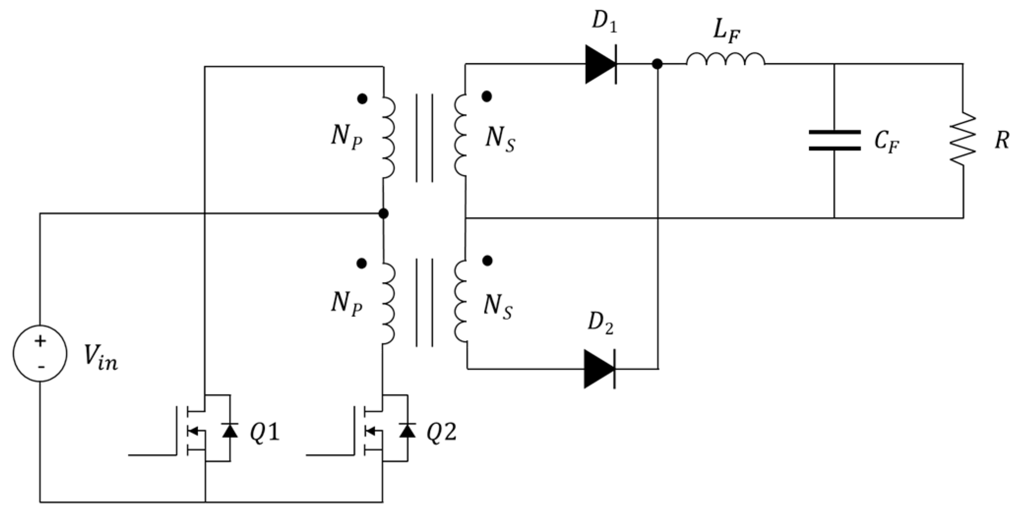
2. Push–Pull Converter: Operating Principle and Non-Ideal Electrical Model

This section describes the operating principle of the push–pull converter and presents its equivalent circuit together with the main non-idealities that determine its equivalent model.

2.1. Push–Pull Converter Operating Principle

The operation of the push–pull converter is determined by the controlled flow of current in the primary transformer circuit and by magnetic induction in the secondary circuit. This control is accomplished by controlled operation of the power switching devices and energy storage in the inductor and capacitor of the output low-pass filter (LF-CF). The electrical schematic of the ideal circuit is shown in Figure 1. In [17] a half-bridge rectifier topology was chosen for the converter output stage (which will be logically maintained in this study), as it reduces the number of semiconductors and their associated losses (which can be considerable especially in high-power buck topologies operating at high output currents) while simplifying circuit analysis and design.
From the ideal circuit diagram (Figure 1), the operation of the push–pull converter is determined by three modes of operation, depending on the state of the power switching devices (Mode 1: Q1 ON and Q2 OFF, Mode 2: Q1 OFF and Q2 ON and Mode 3: Q1 and Q2 OFF).
In modes 1 and 2, the conduction of the power switching device allows current to flow through the corresponding primary winding of the transformer (see Figure 1), magnetising its core. This induces a voltage in the secondary circuit of polarity defined by the point criterion (see Figure 1), which will allow current to flow through one of the branches (through diodes D1 or D2) to the output low-pass filter and the load R.
Finally, during mode 3 operation, the deactivation of both power switching devices prevents current flow through the primary windings, and hence no voltage will be induced in the transformer secondary circuit (see Figure 1). In this case, it is the output low-pass filter (LF and CF) which maintains the output voltage by supplying current to the load. Assuming a continuous conduction mode (CCM) in the output low-pass filter inductor current, it follows that D1 and D2 conduct at the same time and there is current sharing between the two branches.

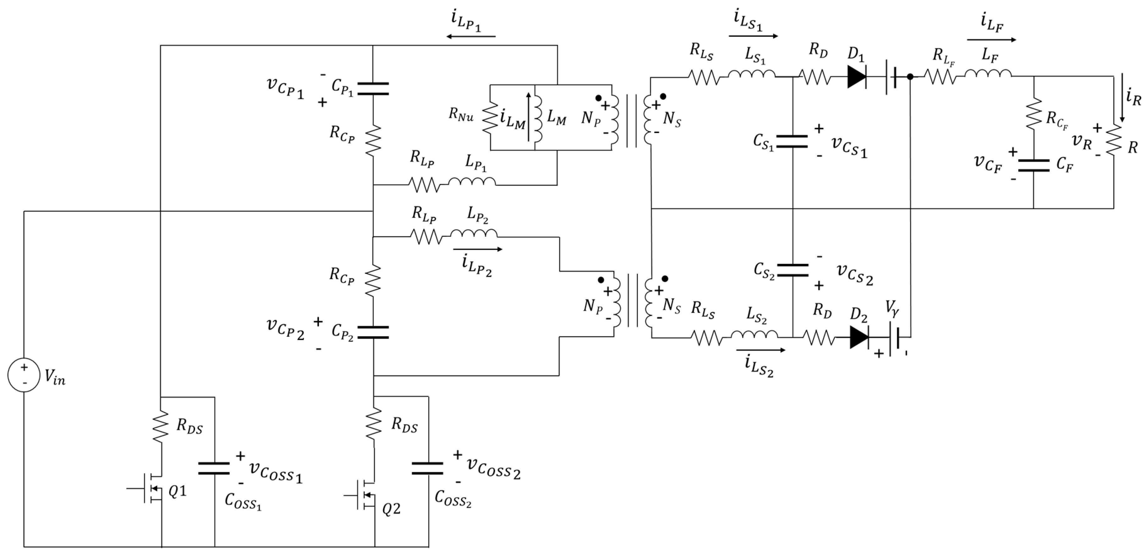
2.2. Non-Ideal Push–Pull Converter Circuit

The electrical circuit in Figure 1 allows modelling the ideal behaviour of the push–pull converter, which is a simple approximation of the actual converter behaviour. To develop an accurate model of the converter, non-idealities associated with the transformer, the power switching devices and the converter output low-pass filter must be considered. With this in mind, the authors developed and validated in [17] the non-ideal model shown in Figure 2, which the authors demonstrated exhibits behaviour very close to the actual circuit of a push–pull converter.
The non-idealities in Figure 2 are as follows (please see list of nomenclature and symbols in this document): for the transformer, the series resistance and the leakage inductances and capacitances of the primary and secondary windings ( R L P , R L S , L P 1,2 , L S 1,2 , C P 1,2  and C S 1,2 , respectively) as well as the core losses associated with the magnetisation current, eddy currents and parasitic fluxes ( L M and R N u ) have been considered.
For power transistors (Mosfets), series drain-sink saturation resistance ( R D S ) and parallel output capacitances ( C O S S 1,2 ) are considered. For rectifier diodes, the series resistance ( R D ) and threshold voltage ( V γ ) are considered.
Finally, for the converter output LC filter, series resistance of both the inductance ( R L F ) and the filter capacitor ( R C F ) are considered.
As stated in [17], because they are considered non-idealities of negligible effect, mainly because they can be avoided with a good design and manufacture of the converter, the following is assumed: As for the transformer, both windings will be identical. In terms of operation, the transformer shall be considered to be fully magnetised and demagnetised in each operating cycle. Likewise, the transformer core will always operate within the linear region of the magnetisation curve, so no core saturation effects will be considered.
Similarly, in the case of power switching devices, it will be considered that the switching times will be negligible with respect to the duty cycle corresponding to the operating frequency. It is also assumed that the power switching devices will be of adequate quality, so their leakage currents will be neglected.
Based on the above, for the complete definition of the non-ideal behaviour of the push–pull converter, the following 14 non-idealities will be considered: R L P , R L S , L P x , L S x , C P x ,   C S x ,   L M ,   R N u ,   R D S , C O S S x , R D ,   V γ ,   R L F   a n d   R C F .

2.3. Non-Ideal Push–Pull Model

The non-ideal model of the converter is obtained from the analysis of the non-ideal equivalent circuit shown in Figure 2 for the operating sequences of the power transistors. Thus, following the modelling proposed in [17] and considering as state variables the inductor currents ( i L P 1 , i L P 2 , i L M , i L S 1 , i L S 2 , i L F ) and the capacitor voltages of the circuit ( v C P 1 , v C P 2 , v C O S S 1 , v C O S S 2 , v C S 1 , v C S 2 , v C F ), the input voltage of the converter as the input of the model ( v i n ) and the converter output voltage and current as the output variables ( v R , i R ), the complete non-ideal model of the push–pull converter calculated in [17] can be written in its state-space representation according to (1):
x k + 1 = A x k + B u k + E y k = C x k + D u ( k )
where k is the sampling time, the matrices A, B, C, D and E can be found in [17], and
x = [ i L P 1 , i L P 2 , i L M , i L S 1 , i L S 2 , i L F , v C P 1 , v C P 2 , v C O S S 1 , v C O S S 2 , v C S 1 , v C S 2 , v C F ] T u k = v i n k y k = v R k i R k T

3. Push–Pull Converter Sizing and Parameterisation

This section presents the step-by-step methodology to obtain the parameters of the non-ideal model of Figure 2 according to Equation (1). Since the main objective of the paper is to evaluate and identify the impact that each non-linearity has on the overall behaviour of the converter output variables, the methodology developed here is based on a compendium of equations proposed and validated in the scientific literature. In order to avoid continuous cuts in the explanations, the meaning of all parameters and variables used in this section can be found in the list detailing the nomenclature and symbols used in this document.

3.1. Transformer Sizing and Parametrisation

3.1.1. Transformer Core

When sizing a transformer, many variables are involved to estimate the proper core size. It is a complex task that requires consideration of the non-linear relationship of the operating power with respect to the area product, core volume and heat dissipation capacity [29]. To facilitate this task, magnetic core manufacturers propose their own methodology for the correct choice of core size for various applications. These methodologies are based on the determination of the minimum core area product ( A P ), defined by the area of the magnetic section ( A E ) and the window area ( A W ) which guarantees the required magnetic flux capacity of the transformer core, assuming its operation in the linear region, for a design power and frequency [30]. In this case, the empirical Equation (2), provided by Unitrode® (Merrimack, NH, USA) and Texas Instruments® (Dallas, TX, USA), will be used to size the cores for the different cases under study. This equation is commonly used in the design of power transformers for switching power supplies [29].
A P = A E · A W = P o K · B · f s w 4 3
For the design of the different transformers, E-type core (widely used in the design of power transformers) of N27 and N87 ferrite materials (MnZn) from TDK Electronics® (Munich, Germany) have been chosen. Zinc-based ferrites are characterised by high saturation flux densities and high magnetic permeability, which favours the reduction of core size and cost [31]. The choice of TDK Electronics® products is justified by the fact that it is a well-known manufacturer in the industry, which also has intuitive and powerful design tools for the calculation of the main parameters of the transformer core.

3.1.2. Number of Primary and Secondary Winding Turns

To calculate the number of turns of the primary and secondary windings of the transformer, Faraday’s law given by Equation (3) will be used. This equation allows to obtain the value of the induced voltage (V) for an inductor with N turns [9]:
V = N Φ t
Particularly for the study of the primary winding, considering that t = t o n and omitting the minus sign, since it only defines the polarity of the induced voltage, (3) can be written as (4):
V P · t o n = N P · Φ = N P · B · A E
Then, considering that   t o n = δ / f s w , (4) can be written as (5):
N P = V P · δ B · A E · f s w
The number of turns of the secondary winding must guarantee the correct conversion ratio of the transformer considering the operating conditions of the converter. Thus, for its calculation, both the ratio between input and output voltage and the predefined maximum duty cycle ( δ m a x ) shall be considered, according to (6).
N S N P = V o 2 V i n · δ m a x N S = N P · V o 2 V i n · δ m a x

3.1.3. Primary and Secondary Windings’ Resistance

The resistance value of the primary and secondary windings is determined by their length, effective cross-section and operating temperature according to Equation (7) [32]:
R w = ρ l w S w 1 + α · T T R e f
The wire length shall be determined by the number of turns of each winding and the core size. Its section will be calculated from the maximum operating current (thermal criterion) that guarantees the integrity of the electrical insulator. In this case, a thermal increase of 60° has been considered for a reference ambient temperature of 20° (maximum operating temperature in permanent regime of 80 °C).
The sizing of the cross-section by thermal criteria depends mainly on the operating current, the arrangement of the conductors in the winding, the number of layers, the thermal resistance of the transformer core, etc. Therefore, it is not easy to obtain a general formulation for the different converter designs. However, since this is not an objective of this work, it has been chosen to use typical experimental effective amperage-section tables for single-pole copper conductors. The values provided by these tables are quite conservative since their determination is based on stringent experimental safety factors.
Finally, to obtain the corrected resistance of the wire, the influence of the frequency on the effective cross-section according to the skin effect will be considered. Knowing the electron decay equation in the conductor cross-section modelled in (8) [33] and assuming that the electrons are concentrated in the effective area given by the skin depth ( ξ ), a correction factor ( κ ) of the resistance as a function of the wire cross-section ( S w ) and the effective cross-section of the wire ( S w e ) can be calculated in (9):
ξ = 2 ρ ( 2 π f s w ) ( μ 0 μ r )
κ = S w S w e = π r 2 π r 2 r ξ 2 = r 2 r 2 r ξ 2
In view of the above, the effective resistance values of the winding considering skin effect are given by (10):
R w e = κ · R w

3.1.4. Leakage Inductances of Transformer Primary and Secondary Windings

The calculation of the leakage inductance of a transformer ( L l k ) is a complex task that is highly dependent on the transformer topology, the winding process and the physical separation between conductors. The influence of these factors determines the three fundamental components of the leakage inductance: the internal leakage inductance ( L i n ), the Yoke leakage inductance ( L y ) and the equivalent leakage inductance ( L e q ) [34].
For a transformer with push–pull topology (separate primary and secondary windings), several works have proposed an analytical solution to determine the fundamental components of the leakage inductance of the transformer windings. A general expression for its calculation, successfully validated experimentally, is proposed in [34] and given by (11):
L l k = 2 ( L i n + L y + L e q )
The expressions proposed in [34] for the calculation of internal leakage inductances and yoke leakage inductances are complex and require previous tests on the transformer, so practical simplifications are required, which, with reasonable accuracy, favour their calculation. Thus, if it is assumed that the primary and secondary windings of the transformer are concentric throughout the window area of the central branch of the transformer core (usual in this type of power transformer) and conductors with reduced insulation thickness (insulating varnish) have been used for their manufacture, the terms associated with the internal leakage inductance and the yoke leakage inductance can be considered negligible with respect to the equivalent leakage inductance term [34]. Therefore, the leakage inductance of the transformer windings ( L P 1,2 and L S 1,2 , see Figure 2) can be calculated from the equivalent leakage inductance equation for this type of transformer topology, according to (12) [34]:
L P , S = 2 · μ 0 · N P x , S x 2 · l a · b w 3 · h w

3.1.5. Parasitic Capacitances of Transformer Primary and Secondary Windings

The transformer primary and secondary inductor windings have a distributed parasitic capacitance defined by the turn-to-turn capacitance between turns of the same layer ( C t t ) , between turns of adjacent layers and between turns and the transformer core shield (if present) [35,36]. The total turn-to-turn distributed capacitance of the primary and secondary windings ( C P x , C S x , respectively; see Figure 2) can be modelled by a parallel capacitance connected between the winding terminals whose value will depend on the thickness of the wire insulation and the winding method used, according to the empirically derived expression (13) [35,36]:
C t t = 0 · l t r · ln D 0 D c + cot 2 cot π 12
where
= a r c o s 1 ln D 0 D c r
To obtain the value of the total parasitic capacitance of the transformer primary and secondary windings ( C P x , C S x , respectively), it is necessary to consider the number of winding layers. Expression (15) gives an estimate of the total parasitic capacitance of the windings as a function of the number of winding layers [35,36]:
C P x , C S x = 1.8300   C t t   ( f o r   s i n g l e-l a y e r   w i n d i n g )   1.3660   C t t   ( f o r   t w o-l a y e r   w i n d i n g ) 0.5733   C t t   ( f o r   t h r e e-l a y e r   w i n d i n g )

3.1.6. Magnetising Resistance

For the calculation of magnetising resistance ( R N u , Figure 2), it is necessary to know the core losses. In the scientific literature, there are different analytical models for the estimation of transformer core losses considering Eddy current losses and hysteresis losses, depending on the type of magnetic core and topology [37,38]. These models are complex to apply and require information obtained from experimental tests on the transformer, which makes them difficult to apply in this study. There are simpler and reasonably accurate traditional models that do not require prior testing to estimate power losses. These simplified models are based on generalised experimental equations, such as the experimental Steinmetz equation (OSE), its modified version (MSE), its general version (GSE) or the improved generalised Steinmetz equation (IGSE) [39,40]. For this study, since real transformers are not available for testing and analysis, to obtain the best possible approximation, core losses were estimated from TDK Electronics® transformer and inductance design software (EPCOS Magnetic Design Tool Ver. 5.5.1.127, compiled on 18 April 2018). The power loss density in the transformer core was calculated considering it to be of the ferrite type, push–pull topology with a duty cycle of 0.45 and a rate operating temperature of 80 °C (usual operating temperature under rate conditions). Considering the power loss density ( P L ) at the rated operating voltage of the transformer and considering the voltage drops in the primary windings of the transformer negligible, the magnetising resistance of the transformer core is given by the expression of the active power dissipated in a resistor, given by (16).
P L · V e = V L N u 2 R N u R N u = V L N u 2 P L · V e

3.1.7. Magnetising Inductance

To calculate the magnetisation inductance of the transformer, according to the basic theory of magnetic components, the electrical-magnetic equivalence of the transformer core (reluctance model) is considered [7,41]. For an E-type core without a gap, an equivalent electrical circuit with three reluctances is obtained (Figure 3). Their values are determined according to the dimensions of the transformer core and its magnetic permeability according to Ohm’s law (17):
R x = l x A x · μ 0 · μ r
Based on the transformer reluctance model (Figure 3) and Ampere’s law, expression (18) calculates the total magnetic flux intensity:
Φ 3 = N P · I L P R 3 + ( R 1 R 2 )
From the concept of inductance, assuming that the transformer leakage inductances are negligible with respect to the value of the magnetising inductance, its value is given by (19):
L M = Φ 3 · N P I P = N P 2 R 3 + R 1 · R 2 R 1 + R 2
where
R 1 = l 1 A 1 · μ o · μ r , R 2 = l 2 A 2 · μ o · μ r ,   R 3 = l 3 A 3 · μ o · μ r

3.2. Sizing and Parameterisation of the Output Low-Pass LC Filter

3.2.1. Low-Pass Filter Inductance

According to Faraday’s law and the operation of the converter, when any of the transistors is on, the relationship between current and voltage at L F (see Figure 2) is given by (21):
v L F = L F d i L F ( t ) d t = L F I L F t
If the internal voltage drops associated with the rectifier diodes, power transistors and transformer primary and secondary windings are neglected (considering ideal components is enough for this analysis), the inductor voltage can be obtained by the difference between the voltage induced in the transformer secondary and the converter output voltage. The transformer secondary voltage can be obtained from the product of the converter input voltage and the transformer ratio (22):
I L F t V L S x V O L F = N S N P V i n V O L F
If t = t o n = δ / f s w , (22) can be written as (23):
L F = N S N P V i n V O δ I L F · f s w
From (23), the inductance value is inversely proportional to the current ripple in the inductor. For its sizing, the direct relationship between inductance and internal resistance has been considered. In view of the above, to reduce the internal resistance of the inductor, a relatively high-current ripple ( I L F = 30%) has been considered. This ripple value can be easily damped with a high-capacity output capacitor (with much lower internal resistance values).

3.2.2. Low-Pass Filter Capacitance

Considering the charge variation in a capacitor, the relationship between current and voltage at C F (see Figure 2) is given by (24):
i C F = C F d i V C F ( t ) d t = C F V C F t
Again, if t = t o n = δ / f s w , if the internal voltage drop of the capacitor is neglected (considering ideal components is sufficient for this analysis) and knowing that the capacitor current is that corresponding to the inductor current ripple, C F is given by (25):
C F = I C F · δ V C F · f s w
From (25), the capacitance value is inversely proportional to the voltage ripple in the capacitor. Knowing that it is essential to keep the converter output voltage stable, a voltage ripple value usually used in power supplies ( V C F = 1%) has been considered.

3.3. Sizing and Parameterisation of the Switching Devices

The main criterion used for the sizing of the switching devices is based on determining the rated operating voltage and current values according to the topology and case under study. It will also be necessary to consider an appropriate switching frequency to minimise the switching losses.
Thus, for both the power transistor and the rectifier diode, the rated voltage value will be determined by the maximum blocking voltage during turn-off. For the current, two limit values must be defined, the average and the peak current, which define the thermal and physical operating limits of the switching device, respectively. Generally, sizing switching devices according to the average current criterion also ensures compliance with the peak current criterion since in power switching devices the peak pulsating current is usually much higher than the steady-state current (on the order of two to three times higher) [42].
Thus, based on the push–pull converter operation, the transistor blocking voltage ( V B Q ) is determined by twice the input voltage (26). The average current ( I Q A v e ) can be calculated from the quotient of the rated design power and the rated input voltage (27). Finally, the peak current is determined by the maximum instantaneous input current of the converter, which is highly dependent on the current ripple imposed by the primary leakage and magnetisation inductances of the transformer:
V B Q = 2 · V i n
I Q A v e = P O V i n
In the case of the rectifier diode, the blocking voltage ( V B D ) is determined by twice the input voltage multiplied by the transformation ratio (28). On the other hand, the average current ( I D A v e ) can be calculated from the quotient between the rated design power and the output voltage, considering the current sharing between the branches of the full-wave rectifier (29). Finally, the peak current is determined by the maximum instantaneous output current of the converter, which is highly dependent on the current ripple imposed by the low-pass filter inductance:
V B D = 2 · V i n · N S N P
I D A v e = P O 2 · V i n
Finally, considering the non-ideal model of the switching devices, the main parameters (see Figure 2), R D S and C O S S for the transistors and V γ and R D for the rectifier diodes, can be obtained directly from their datasheets for the expected operating voltage and current conditions.

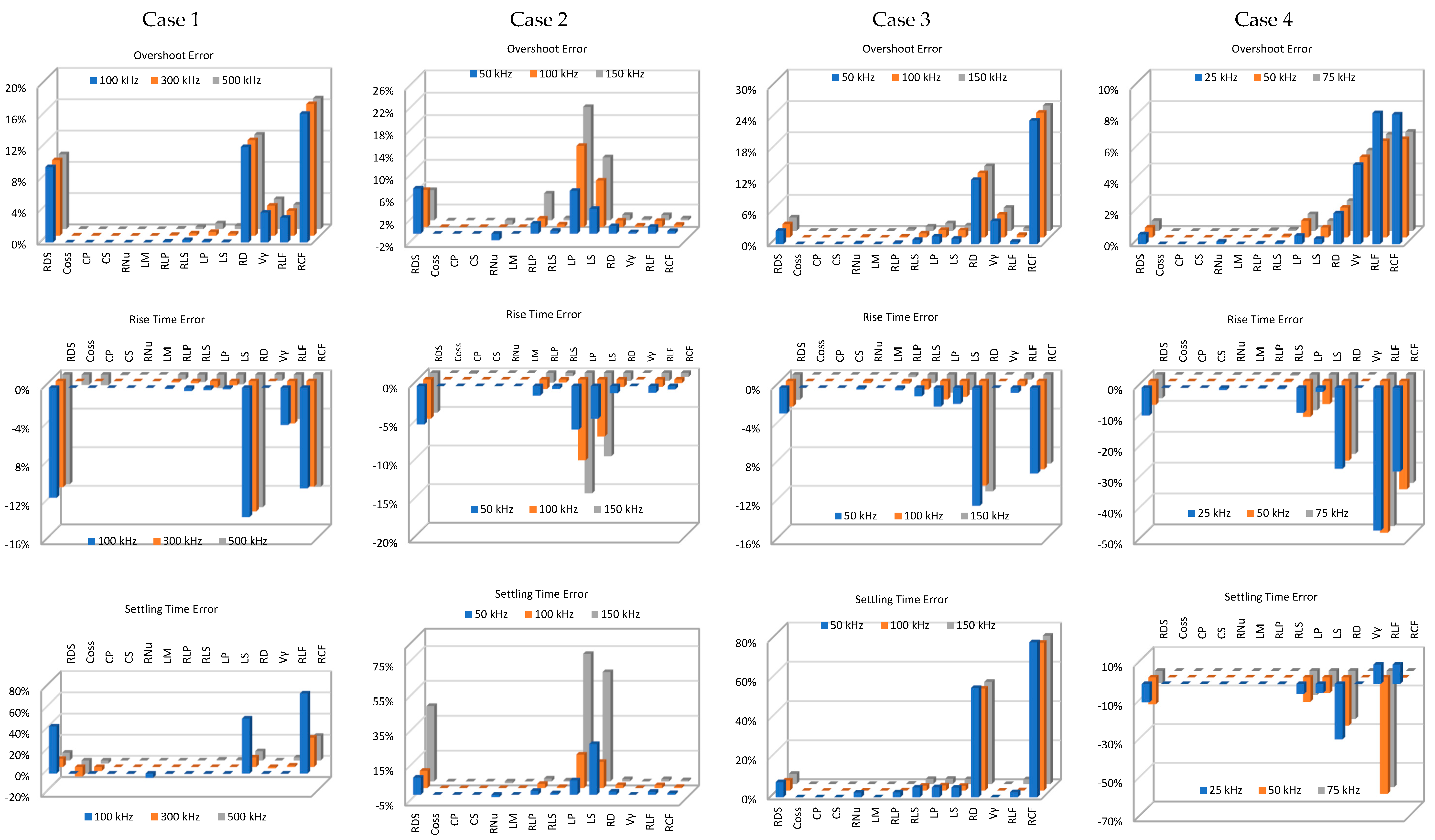
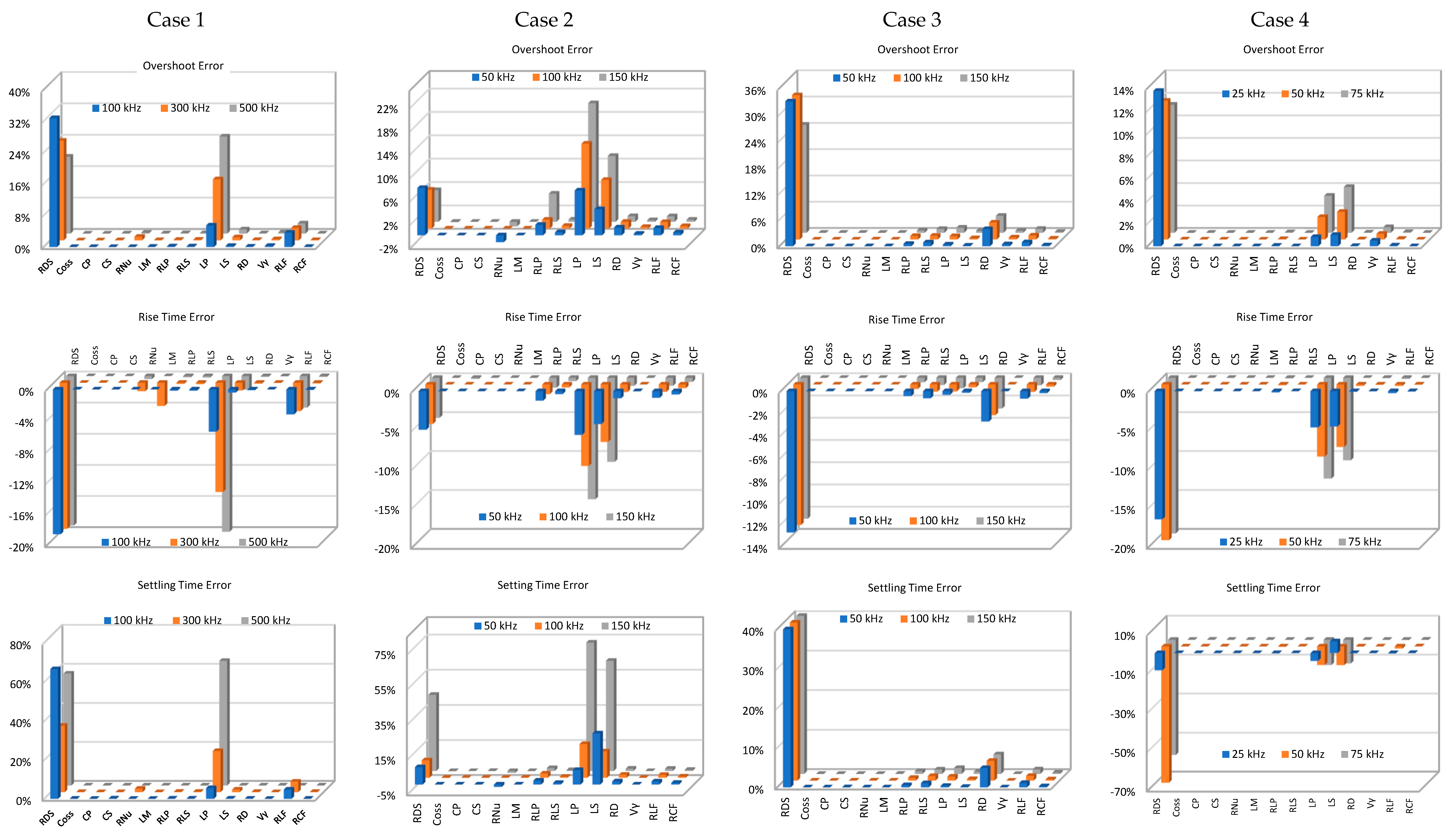
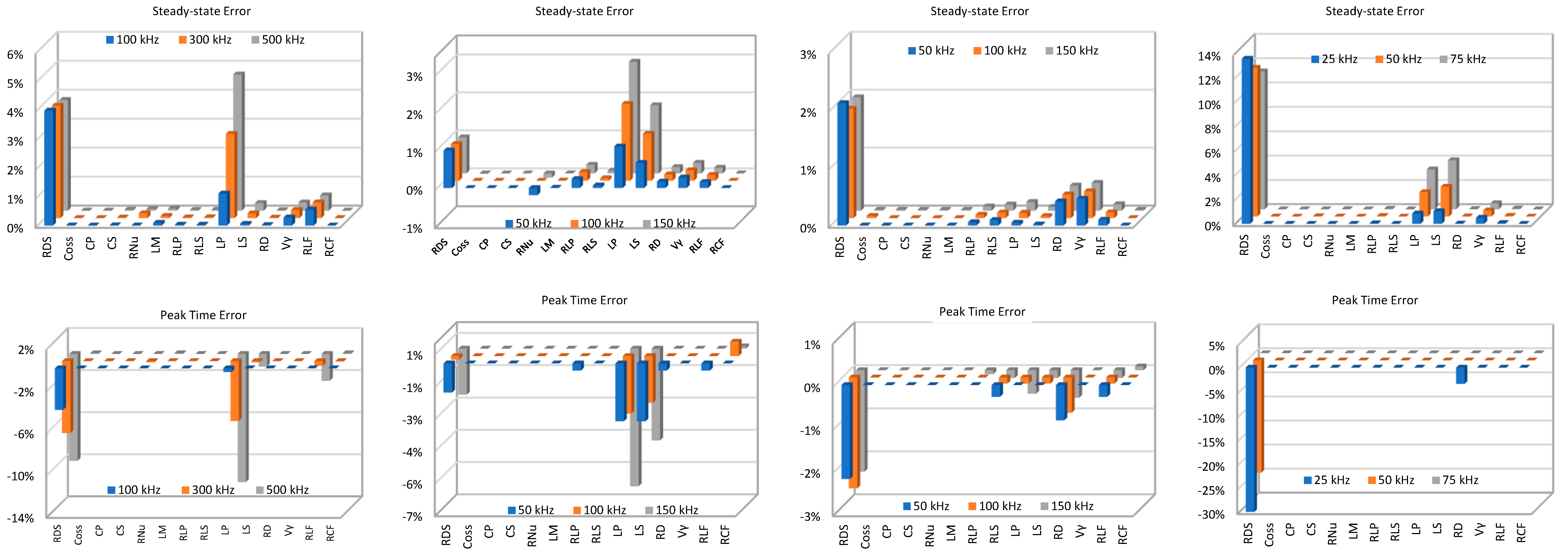
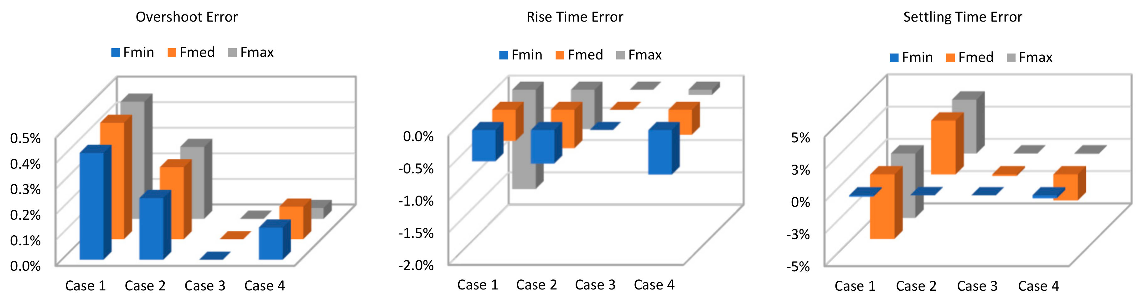
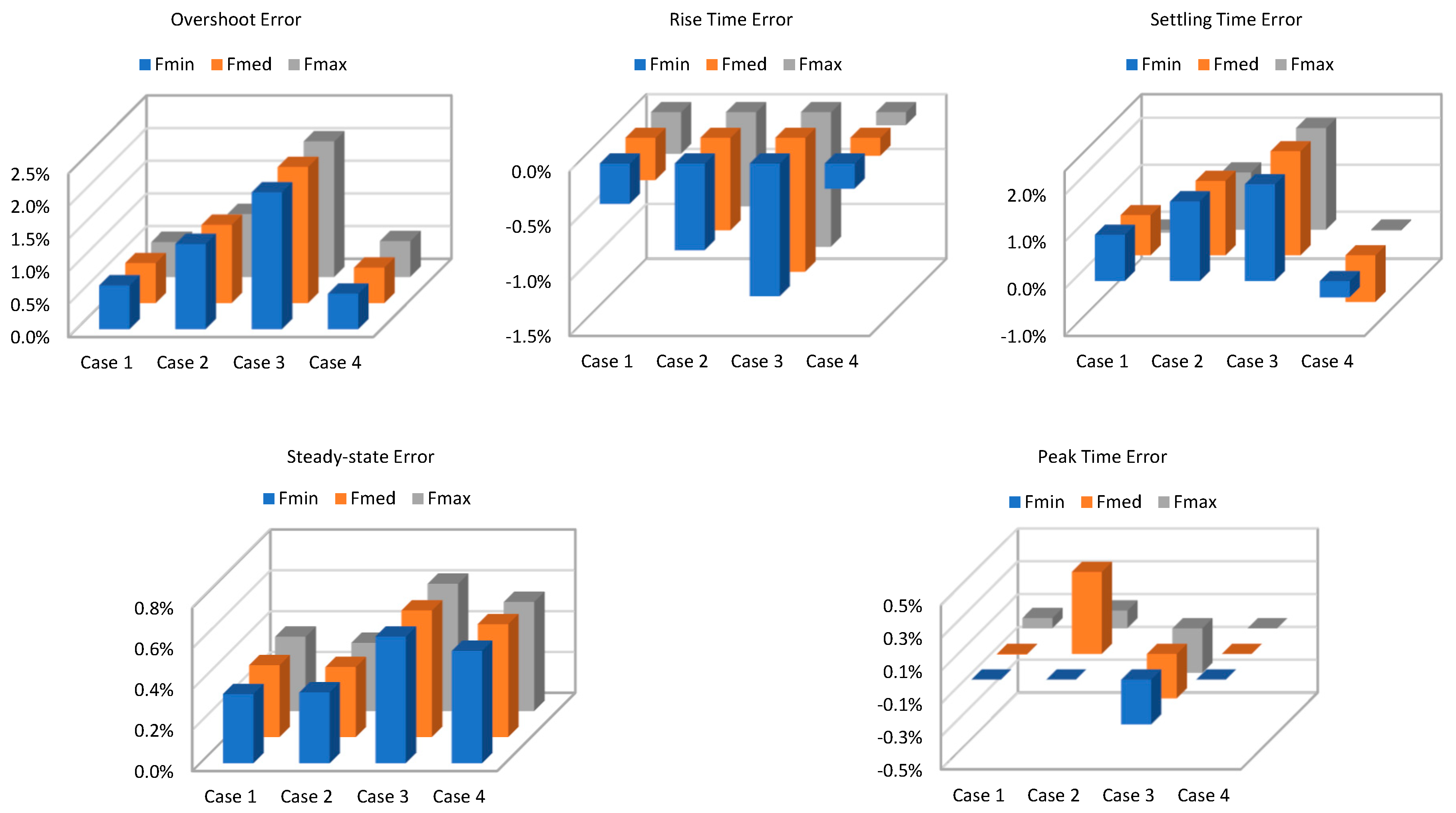
4. Sensitivity Analysis

4.1. Push–Pull Converter Design: Case Studies

To determine the best trade-off between complexity and practical viability of the model in terms of topology, power and operating frequency, a sensitivity analysis is required to determine the influence of each non-ideality on its dynamic response. Thus, based on Equations (2)–(29), two topologies of push–pull converters, boost and buck, have been designed for four power ranges under study (cases), and three ranges of typical operating frequencies used in the scientific literature and in commercial converters. This determines a total of 24 different converter cases to be studied.
Specifically, for the design of the buck topology, typical voltage values based on single-phase power supplies of 300 VDC input and a converter output of 30 VDC have been considered. In contrast, for the case of the boost topology, practical cases of integration of low-voltage renewable energy sources at 30 VDC input and a converter output of 300 VDC have been considered. Finally, due to the small number of applications, extreme low-power applications (<1 W) and operating frequencies above 500 kHz have not been considered in this study. The four cases under study are as follows:
  • Case 1: Very low power (1 W–10 W) and operating frequencies of 100 kHz, 300 kHz and 500 kHz.
  • Case 2: Low power (10 W–100 W) and operating frequencies of 50 kHz, 75 kHz and 150 kHz.
  • Case 3: Medium power (100 W–1 kW) and operating frequencies of 50 kHz, 75 kHz and 150 kHz.
  • Case 4: High power (1 W–10 kW) and operating frequencies of 25 kHz, 50 kHz and 75 kHz.
For the sizing of each converter for each topology and case, the design power has been considered as the upper power limit of the case under study, as well as the lowest operating frequency of the established range, being the most restrictive conditions. Likewise, a conservative maximum duty cycle of 0.45 has been considered to avoid short circuits due to operating at duty cycles close to 0.5.
For the design of the different converters according to the established cases and considerations, a market study was carried out based on commercial power electronic devices from widely known manufacturers. From this preliminary study, a first selection of suitable devices was obtained, considering different models but with a similar performance and parameters. Finally, the components were selected considering that their nominal parameters would fit the parameters calculated for each topology, buck and boost, and for each power range under study. Once the components were selected, their main parameters were obtained from the nominal values given in their datasheets in the case of the power switching devices and the output low-pass filter components and from Equations (7)–(20) for the power transformer. Table 1, Table 2, Table 3 and Table 4 show the main parameters of the converters designed from the selected components for both topologies and cases.

4.2. Sensitivity Analysis

This analysis consists of a comparison by simulation of the main characteristic parameters associated with the dynamic and steady-state response of the output variable (output voltage, V O ) of a simplified converter model with respect to that of the expected behaviour of the full converter model (reference model) for a step-type input signal.
Due to the nature of the proposed research, it might be considered of interest to work with real converters instead of simulations. However, this would have required the construction of 24 converters. This is an unaffordable cost due to the purchase of devices, acquisition cards, controller circuits, etc. on the one hand and the enormous number of working hours involved on the other. But also, it is not considered necessary, since, as demonstrated in [17], the performance of the complete non-ideal model of the converter fits almost perfectly to the real case. In fact, the complete non-ideal model of the converter was validated against a real converter. Consequently, it is sufficient to use this model, already validated (which can be considered as a reference or benchmark), to analyse the true influence of the non-linearity not taken into account in each case of sensitivity analysis.
The methodology proposed for the sensitivity analysis is based on cancelling out in each simulation of the complete non-ideal model of the converter the effect of a specific non-ideality from those defined in Section 2.2. For this purpose, the terms associated with the non-ideality under study (the one not taken into account in each case) are removed from the full reference model [17], i.e., the corresponding row or column is removed from the model, which reduces the order of (1) from 13 to minus.
In this way, it is possible, by comparison with the full reference model, to isolate the effect that each non-ideality has on the converter response. To quantify this effect, it is necessary to calculate certain magnitudes of percentage errors that determine the differences between the behaviour of the output variable of each simplified model and the reference one (for each non-ideality and case study). Although the reference model is of high order (13th order), the dynamic behaviour of the output parameters, voltage and current is mainly determined by the output low-pass filter (LC circuit). Consequently, the dynamics of the converter output variables can be expected to follow a response similar to that of a second-order system. For this reason, the errors chosen for the analysis are the usual ones in a second-order system: overshoot error, rise time error, fall time error, steady-state error and peak time error. The results of more than 330 simulations performed in a Matlab® Ver R2019a environment for all the cases under study, operating frequencies and topologies, buck and boost are shown in Figure 4 and Figure 5, respectively.

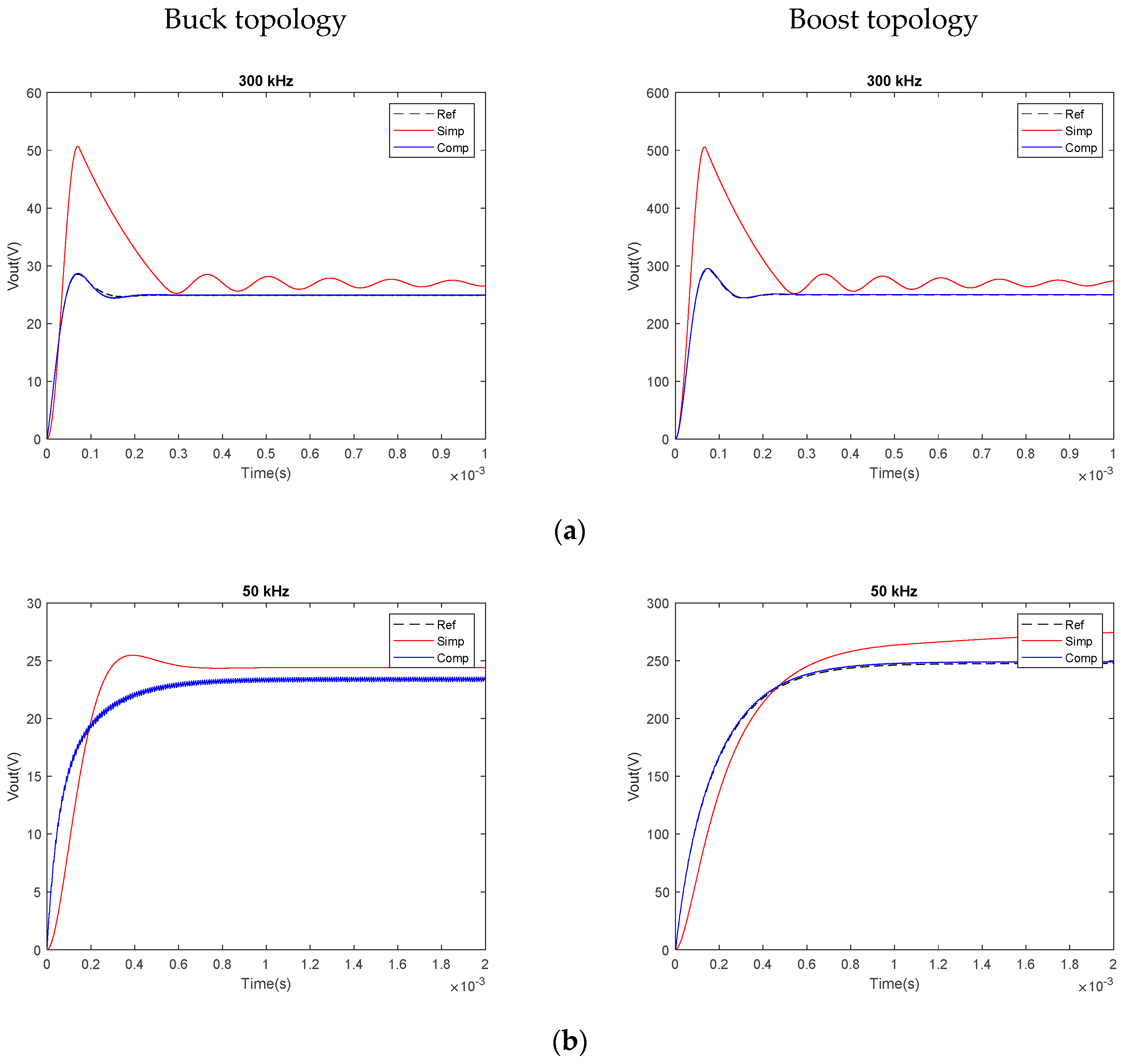
5. Discussion and Derivation of the Models That Meet the Trade-Off between Complexity and Practical Feasibility

In this section, a detailed analysis of the results obtained from the sensitivity analysis is carried out. In particular, the effects that each non-ideality contributes to the converter behaviour are studied. To this end, an analysis is made of the percentage errors shown in Figure 4 and Figure 5, which quantify the difference in the dynamic and steady-state response of each simplified model (for each non-ideality cancelled) with respect to the expected response (that of the reference model). From this analysis, the key cause–effect relationships are obtained for the subsequent definition of the simplified equivalent circuits of the converter and, ultimately, of the models that fulfil the trade-off between complexity and practical feasibility.

5.1. Discussion

Based on the results obtained from the sensitivity analysis, Figure 4 and Figure 5, conclusions can be drawn to design push–pull converter models that meet the balance between complexity and practical feasibility according to the topology and nominal operating conditions. The effect of each non-ideality on the dynamic and steady-state response of the converter will be analysed element by element. To this end, it is important to note that the dynamic response of the converter’s internal variables (voltages and currents), and ultimately the output voltage will be determined by the dynamics provided by the energy storage elements (inductors and capacitors) and the series resistors that limit their charge and discharge dynamics. On the other hand, the steady-state response will be determined both by the voltage drops in resistors and diodes (losses), as well as the influence of the value of the inductances and capacitors. This is justified if it is considered that their values, together with those of the series resistors, determine the variation of the voltage and current variables and, depending on the duty cycle, the final value of these magnitudes.
Firstly, the effect of transformer non-idealities (core and windings) on the response of the converter output voltage will be analysed. Table 5 and Table 6 show, easily and qualitatively, the quantitative results of Figure 4 and Figure 5. They show the effect that each non-ideality has on the dynamic and steady-state response of the converter for each topology and case under study. The results of these tables are the basis for the design of the simplified equivalent models of the push–pull converter. Specifically, in Table 5 and Table 6, a colour intensity criterion is used to represent the effect that each non-ideality has on the converter output variable: the higher the colour intensity, the greater the effect and vice versa. The criterion for defining the intensity of the effect is as follows: large if any absolute error magnitude is greater than 10%, moderate if it is less than 10% and greater than 5%, reduced if it is less than 5% and greater than 2% and negligible if it is less than 2%.
Considering the transformer core, it is shown that its correct sizing in terms of constituent magnetic material and area product allows the effect of the core non-idealities ( L M and R N u ) on the dynamic and steady-state response of the converter to be negligible (see errors for L M and R N u in Figure 4 and Figure 5 and Table 5 and Table 6). The reduced influence on the dynamic response is due to the high value of the magnetising inductance ( L M ) with respect to those of the windings ( L P ). According to expressions (21) and (22), and for the switching frequencies of the converters, its effect on the transformer primary current dynamics and, consequently, on the voltage induced in the secondary is negligible. Finally, the reduced impact on the steady-state response is justified because the losses associated with the core (due to a high value of R N u ) are negligible with respect to the rest of the converter losses.
Similarly, the correct sizing of the transformer primary and secondary winding conductors determines an equivalent resistance ( R L P and R L S , respectively) that are negligible with respect to the internal resistances of the power switching devices ( R D S ). This implies that their influence on the dynamic behaviour of the transformer primary current and, consequently, on the voltage induced in the secondary is very small. Similarly, the reduced values of R L P and R L S imply reduced transformer voltage drops (losses), which determines the reduced impact on the steady-state response of the output voltage (see errors for R L P and R L S in Figure 4 and Figure 5 and Table 5 and Table 6).
On the other hand, L P and L S affect the dynamic and steady-state response of the converter. Considering the effect on both converter topologies, L P limits the slope of the transformer primary magnetising current due to the opposite induced voltage between its terminals (2): the higher its value, the lower its slope and the induced magnetic flux. This results in a lower induced voltage on the transformer secondary. L S similarly affects the current dynamics of the transformer secondary circuit. A high value increases the opposite induced voltage at its terminals, which reduces the slope of the secondary current and its final value. This causes variations in the dynamic response and a reduction in the steady-state value of the converter output voltage.
Based on the above, the effect that each non-ideality has on the converter response depends on the value of the self-inductance coefficient of L P and L S (highly dependent on the winding method and other factors), the operating frequency and the operating current in both the primary and secondary circuits of the transformer (see errors for L P and L S in Figure 4 and Figure 5). Therefore, it is complex to make a statement about the influence of these parameters on a certain topology under certain operating conditions. A general solution is to always consider these non-idealities in the design of the converter model.
Finally, although the values of the leakage capacitances of the transformer windings ( C P x and C S x ) depend on the method of winding the conductors, the number of layers, the insulation thickness, the use of shielding, etc., the values obtained are usually much lower than those of the output capacitances of switching devices and the output filter capacitance (see Table 1, Table 2, Table 3 and Table 4). Therefore, their effect on the converter dynamics for the switching frequencies under study can be considered negligible (see errors for C P x and C S x in Figure 4 and Figure 5).
Considering the results of the above analysis, the non-idealities of the transformer core ( L M and R N u ),and the winding resistances ( R L P and R L S ) and leakage capacitances ( C P x and C S x ) can be eliminated from the equivalent simplified model for all cases under study (see Figure 4 and Figure 5). This simplification cannot be applied to the primary and secondary winding leakage inductances ( L P and L S ), whose influence depends on the converter topology, operating power and switching frequency (see Figure 4 and Figure 5).
Considering power switching devices and, first, power transistors (Mosfets), the effect of non-idealities, R D S and C O S S x will be analysed. As explained above, R D S affects both the dynamic and steady-state behaviour of the converter. The dynamics of the transformer primary variables are determined by the resistors R D S   and R L P , which determine the dynamics of the core magnetisation process and the energisation of the transformer primary winding leakage inductances. This follows from the analysis of the RLC circuit generated in the transformer primary by R D S , R L P , L P and C O S S x (see Figure 2).
In view of the above, it is the ratio between R D S   and R L P which determines their effect on the dynamic behaviour of the converter. An example of this can be seen in the dynamic response for the buck topology cases (Figure 4), where R D S , several orders higher than R L P (see Table 1, Table 2, Table 3 and Table 4), imposes the dynamics of the magnetising current flow and has a more noticeable effect on the dynamic behaviour of the converter (see the errors for R D S   in Figure 4 and Figure 5 and Table 5 and Table 6).
Finally, the effect on the steady-state response is determined by the voltage drop in R D S , which reduces the effective input voltage at the primary of the transformer. This has a negative effect on the voltage induced in the secondary windings and therefore on the steady-state output voltage value of the converter. This effect is more pronounced the higher the operating current of the transistor, i.e., the higher the rated operating power of the converter. These effects can be seen in the results obtained for both topologies, being more prominent for the boost topology, as it operates with higher current in the primary circuit (see errors for R D S   in Figure 4 and Figure 5 and Table 5 and Table 6).
Although C O S S x can reach relatively high values compared to the leakage capacitances of the transformer primary windings, it is true that there is a direct relationship between its value and the operating power of the switching device: the higher the working power, the higher the output capacitance (see Table 1, Table 2, Table 3 and Table 4). Although this may a priori be a drawback, this is an advantage since for high-power applications their operating frequencies are usually relatively low and makes their effect on the converter dynamics negligible (see errors for C O S S x in Figure 4 and Figure 5 and Table 5 and Table 6).
In the case of the rectifier diode, its internal resistance and threshold voltage influence the steady-state response of the converter, since these non-idealities are reflected as voltage drops (fixed or variable) as a function of the transformer secondary current (see errors for R D and V γ in Figure 4 and Figure 5 and Table 5 and Table 6). Therefore, its effect is more pronounced in cases where the secondary current is higher. This explains why the effect of R D and V γ is greater in the buck topology than in the boost, as well as for the high-power cases, since a voltage drop causes a considerable steady-state error in the output variable, considering the percentage ratio with respect to the nominal output voltage of the converter.
Similar to the effect that R D S has on the dynamics of the transformer primary circuit, R D together with R L S has an effect on the dynamics of the output low-pass filter energisation process. This is deduced from the analysis of the RLC circuit generated in the transformer secondary by R D , R L S , L F and C F (see Figure 2). In view of the above, it is the ratio between R D and R L S which determines their effect on the dynamic behaviour of the converter. An example of this can be seen in the dynamic response for the buck topology cases (Figure 4), where R D , several orders higher than R L S (see Table 1, Table 2, Table 3 and Table 4), imposes the dynamics of the output LC filter and has a more noticeable effect on the dynamic behaviour of the converter (see the errors for R D in Figure 4 and Figure 5 and Table 5 and Table 6).
Finally, the effect of the non-idealities associated with the LC output filter will be considered. The non-idealities associated with R L F and R C F have a negative impact on the dynamic and steady-state behaviour of the converter. With respect to the dynamic response, both R L F and R C F influence the dynamics of the energisation process of the low-pass filter inductor and capacitor, respectively. Their effect on the output low-pass filter dynamics depends on the ratio of R D and R L S x , as well as the converter operating power and frequency (see Table 1, Table 2, Table 3 and Table 4 and the errors for R L F and R C F in Figure 4 and Figure 5 and Table 5 and Table 6). The higher their values, the greater the effect on the converter dynamics.
Finally, R L F and R C F affect the steady-state behaviour of the converter due to the voltage drop, which is a function of the current flows in the operation of the low-pass filter. Thus, as with the non-ideality R D , this effect is proportional to the operating current in the secondary circuit. Therefore, R L F and R C F have a noticeable effect for the buck topology and a negligible one for the boost topology (see errors for R L F and R C F in Figure 4 and Figure 5 and Table 5 and Table 6).

5.2. Simplified Models

From the analysis carried out, it is easy to deduce the models that are sufficiently accurate and simpler than the full state-space model developed in [17] (referred to as the reference model). Thus, for the push–pull buck topology, the following non-idealities must be taken into account: switching devices ( R D S ), HF transformer ( L P x and L S x ), rectifier diodes ( R D and V γ ) and output LC filter ( R L F and R C F ). On the other hand, for the push–pull boost topology, switching devices ( R D S ), HF transformer ( L P x and L S x ), rectifier diodes ( R D ) and output LC filter ( R L F ) must be taken into account. Based on the above, the simplified non-ideal equivalent circuits for the push–pull buck and boost topologies are shown in Figure 6a,b, respectively. This allows to simplify the state-space model (1) so that now the state vector will be x s = [ i L P 1 , i L P 2 , i L S 1 , i L S 2 , i L F , v C F ] T , remaining unchanged with respect to u k and y k . This makes it possible to reduce the model order from thirteen to six. To do this, simply cancel the terms of matrices A, B, C, D and E of the reference (full) model (1) associated with those state variables that are not present in the simplified state vector x s .
Finally, to demonstrate the practical application of the results obtained from the sensitivity analysis, the dynamic and steady-state response of the simplified models was compared with that obtained from the reference model for a step-type input signal.
Figure 7 and Figure 8 show the percentage errors of the dynamic and steady-state response of the simplified models for each case of the buck and boost topologies, respectively. Figure 9 shows the time response and the corresponding validation of the simplified model (Simp) for cases 1 (a) and 4 (b) with respect to the reference model (Ref) and the ideal model (Ideal) for the central values of the switching frequency range for each case and both topologies.
Note that the absolute error percentages shown in Figure 7 and Figure 8 are in all cases lower than five. Likewise, Figure 9 verifies that the dynamic and steady-state behaviour of the simplified models show a similar profile to the reference model and in turn show much higher performances than the ideal model of Figure 1 (the most widespread in the scientific literature).
Based on the results, it is shown that the sensitivity analysis developed for the push–pull converter topology is a very powerful tool for the definition of reduced-order control-oriented models for applications where simplicity and accuracy are fundamental requirements.

6. Conclusions and Future Works

This paper presents a methodology for obtaining simple and sufficiently accurate simplified models of the push–pull converter from its full non-ideal equivalent model.
Unlike the works reviewed in the scientific literature, which present simplified models for specific applications (without general validity), this paper proposes a methodology for obtaining simplified models based on the development of a sensitivity analysis that allows identifying the effect that each non-ideality of the actual (physical) converter has on the response of the simplified model. To obtain these simplified models, the absolute percentage errors of the dynamic response with respect to the reference model behaviour are analysed, considering for their definition those non-idealities whose effect (error) is perceptible in practice.
The performance of the simplified models was evaluated and validated by comparison with respect to the dynamic and steady-state response of the full non-ideal (reference) model, showing absolute percentage errors in all cases below 5%, as well as a dynamic response very similar to that of the reference model.
In view of the analysis carried out, it is concluded that the use of the proposed methodology, based on the use of a sensitivity analysis, allows defining, quantifying and assessing the effect of each non-ideality of the actual (physical) converter to obtain simple and very accurate simplified models of the push–pull converter.
Future work from this research focuses on the application of the simplified models obtained for the design of model-based controllers with the aim of improving the performance of the controller–converter set.

Author Contributions

Methodology, F.J.V.; Software, F.S.; Formal analysis, J.M.A.; Investigation, F.J.V., J.M.A. and F.S.; Writing—original draft, F.J.V. and F.S.; Writing—review & editing, J.M.A.; Supervision, J.M.A. All authors have read and agreed to the published version of the manuscript.

Funding

This work is a contribution of the PID2020-116616RB-C31 Project supported by the Spanish Ministry of Economy and Competitiveness, by the P20_00730 Project supported by Regional Andalusian Government under the European Union Regional Development Fund. Funding for open access charge: Universidad de Huelva/CBUA.

Institutional Review Board Statement

Not applicable.

Informed Consent Statement

Not applicable.

Data Availability Statement

The original contributions presented in the study are included in the article, further inquiries can be directed to the corresponding author.

Conflicts of Interest

The authors declare no conflict of interest.

Nomenclature and Symbols

A E Core magnetic cross-section area (cm2)
α Temperature coefficient of conductive material (3.9 · 10 3   C 1 for copper)
A P Core area product (cm4)
A W Window area available for the winding (cm2)
A x Area of E-type transformer reluctance (m2)
b w Core window width along x axis (m)
C F Filter capacitor (F)
C O S S x Mosfet output capacitance (F); x = 1, 2
C P x Parasitic primary winding capacitance (F); x = 1, 2
C S x Parasitic secondary winding capacitance (F); x = 1, 2
C t t Total parasitic turn-to-turn capacitance of the transformer winding (F)
δ Duty cycle
D C Total conductor diameter excluding insulation thickness (mm)
D x Output branch circulation diodes; x = 1, 2
D 0 Overall conductor diameter including insulation thickness (mm)
B Flux density deviation swing (Tesla, T)
I L F Filter inductor ripple current (A)
V C F Filter capacitor ripple voltage (V)
0 Vacuum electric permittivity (8.8542 · 10−15 F/mm)
r Relative electrical permittivity of the electrical insulator (3.5)
f s w Switching frequency (Hz)
h w Core window height (m)
κ Correction factor for the effective conductor cross-section of the windings
I x A v e Average operating current of switching devices (A), x = Q (transistor), D (rectifier diode)
I C F Filter capacitor current (A)
I L F Filter inductance current (A)
K Parameter associated with the converter topology (0.017 in this case)
l a Average turn length of secondary windings (m)
L e q Equivalent leakage inductance (F)
L F Filter inductance (H)
L i n Internal leakage inductance (F)
L l k Leakage inductance of a transformer winding (F)
L M Leakage inductance due to core magnetising losses (H)
L P x Leakage inductance of the primary winding (H); x = 1, 2
L S x Leakage inductance of the secondary winding (H); x = 1, 2
l t Turn length (mm)
l x Length of E-type transformer reluctance (m2)
l w Length of the windings (m)
L y Yoke leakage inductance (F)
μ 0 Vacuum magnetic permeability ( 4 · π · 10 7 H/m)
μ r Relative magnetic permeability of the conductive material
MPPTMaximum Power Point Tracking
N P Number of turns of the primary winding
N S Number of turns of the secondary winding
P L Transformer core power losses density (W/m3)
P O Output power of the converter (W)
PVPhotovoltaic
Q x Mosfet; x = 1, 2
r Wire radius of transformer windings (m)
R Load resistor (Ω)
R C F Filter capacitor series resistor (Ω)
R D Diode series resistor (Ω)
R D S Mosfet drain-sink resistance (Ω)
R x Equivalent reluctance of transformer sections (A·t/Weber)
R L F Filter inductor series resistor (Ω)
R L P Primary winding resistor (Ω)
R L S Secondary winding resistor (Ω)
R N u Magnetisation resistance related to core losses (Ω)
R w Resistance of the conductors of the transformer windings (Ω)
R w e Effective resistance of the conductors of the transformer windings (Ω)
ρ Resistivity of the conductive material ( 1.71 · 10 8   · m for copper)
S w Cross-section of the conductive material of transformer windings (m2)
S w e Effective cross-section of the conductive material of transformer windings (m2)
T Operating temperature of conductive material (°C)
t o n Activation time of any of the converter electronic switches
T R e f Reference temperature of conductive material (°C)
Φ Magnetic flux intensity (Wb)
V B Q Blocking voltage of switching devices (V), x = Q (transistor), D (rectifier diode)
V C F Filter capacitor voltage (V)
V e Transformer core effective volume (m3)
V γ Diode forward voltage (V)
V i n Converter input voltage (V)
V L F Filter inductance voltage (V)
V L P Leakage inductance of the primary winding voltage (V)
V L S Leakage inductance of the secondary winding voltage (V)
V R N u Magnetisation resistance voltage (V)
V O Converter output voltage (V)
V P Primary winding voltage (V)
ξ Skin depth inside the conductor above which the electron flow rate is reduced to 63% (m)

References

  1. Vacheva, G.I.; Genev, K.; Hinov, N.L. Modeling and Simulation of DC-DC Push-Pull Converter. In Proceedings of the 57th International Scientific Conference on Information, Communication and Energy Systems and Technologies (ICEST), Ohrid, North Macedonia, 16–18 June 2022; pp. 22–25. [Google Scholar]
  2. Liang, T.J.; Lee, J.H.; Chen, S.M.; Chen, J.F.; Yang, L.S. Novel isolated high-step-Up DC-DC converter with voltage lift. IEEE Trans. Ind. Electron. 2013, 60, 1483–1491. [Google Scholar] [CrossRef]
  3. Zhang, H.; Quan, L.; Gao, Y. Dynamic modelling and small signal analysis of push-pull bidirectional DC-DC converter. Comput. Model. New Technol. 2014, 18, 14–18. [Google Scholar]
  4. Ivanovic, Z.; Knezic, M. Modeling Push–Pull Converter for Efficiency Improvement. Electronics 2022, 11, 2713. [Google Scholar] [CrossRef]
  5. Yisheng, Y. A parallel soft-switching push-pull converter applied in automotive inverters. In Proceedings of the 2nd International Symposium on Power Electronics for Distributed Generation Systems, PEDG 2010, Hefei, China, 16–18 June 2010; pp. 423–425. [Google Scholar] [CrossRef]
  6. Camilo, J.C.; Guedes, T.; Fernandes, D.A.; Melo, J.D.; Costa, F.F.; Sguarezi Filho, A.J. A maximum power point tracking for photovoltaic systems based on Monod equation. Renew. Energy 2019, 130, 428–438. [Google Scholar] [CrossRef]
  7. Zhang, Z.; Thomsen, O.C.; Andersen, M.A.E. Optimal design of a push-pull-forward half-bridge (PPFHB) bidirectional DC-DC converter with variable input voltage. IEEE Trans. Ind. Electron. 2012, 59, 2761–2771. [Google Scholar] [CrossRef]
  8. Köse, H.; Aydemir, M.T. Design and implementation of a 22 kW full-bridge push–pull series partial power converter for stationary battery energy storage system with battery charger. Meas. Control 2020, 53, 1454–1464. [Google Scholar] [CrossRef]
  9. Andújar, J.M.; Vivas, F.J.; Segura, F.; Calderón, A.J. Integration of air-cooled multi-stack polymer electrolyte fuel cell systems into renewable microgrids. Int. J. Electr. Power Energy Syst. 2022, 142, 108305. [Google Scholar] [CrossRef]
  10. Gómez, J.M.E.; Piña, A.J.B.; Aranda, E.D.; Márquez, J.M.A. Theoretical assessment of DC/DC power converters’ basic topologies. A common static model. Appl. Sci. 2017, 8, 19. [Google Scholar] [CrossRef]
  11. Chandresh, K.; Makwana, M.V.; Rathod, R.N. Design and Implementation of Soft Switching based Push Pull Converter for LED Application. In Proceedings of the 2019 IEEE International Conference on Innovations in Communication, Computing and Instrumentation, ICCI 2019, Chennai, India, 23 March 2019; pp. 132–135. [Google Scholar] [CrossRef]
  12. Nugraha, S.D.; Qudsi, O.A.; Yanaratri, D.S.; Sunarno, E.; Sudiharto, I. MPPT-current fed push pull converter for DC bus source on solar home application. In Proceedings of the 2017 2nd International Conferences on Information Technology, Information Systems and Electrical Engineering, ICITISEE, Yogyakarta, Indonesia, 1–2 November 2018; pp. 378–383. [Google Scholar] [CrossRef]
  13. Meshael, H.; Elkhateb, A.; Best, R. Topologies and Design Characteristics of Isolated High Step-Up DC–DC Converters for Photovoltaic Systems. Electronics 2023, 12, 3913. [Google Scholar] [CrossRef]
  14. Jayasree, K.S.; Chandrakala, K.R.M.V. Active Cell Balancing Technique for Improved Charge Equalization in Lithium-Ion Battery Stack. In Proceedings of the 4th International Conference on Recent Developments in Control, Automation & Power Engineering, Noida, India, 7–8 October 2021. [Google Scholar]
  15. Suprabha Padiyar, U.; Kalpana, R. Design & Analysis of Push-pull Converter Fed Battery Charger for Electric Vehicle Application. In Proceedings of the PESGRE 2022—IEEE International Conference on “Power Electronics, Smart Grid, and Renewable Energy”, Trivandrum, India, 2–5 January 2022; pp. 1–6. [Google Scholar] [CrossRef]
  16. Wang, Z.; Su, X.; Zeng, N.; Jiang, J. Overview of Isolated Bidirectional DC–DC Converter Topology and Switching Strategies for Electric Vehicle Applications. Energies 2024, 17, 2434. [Google Scholar] [CrossRef]
  17. Vivas, F.J.; Segura, F.; Andújar, J.M. Generalized, Complete and Accurate Modeling of Non-Ideal Push–Pull Converters for Power System Analysis and Control. Appl. Sci. 2023, 13, 10982. [Google Scholar] [CrossRef]
  18. Petit, P.; Aillerie, M.; Sawicki, J.P.; Charles, J.P. Push-pull converter for high efficiency photovoltaic conversion. Energy Procedia 2012, 18, 1583–1592. [Google Scholar] [CrossRef]
  19. Trujillo, C.L.; Velasco, D.; Figueres, E.; Garcerá, G.; Ortega, R. Modeling and control of a push-pull converter for photovoltaic microinverters operating in island mode. Appl. Energy 2011, 88, 2824–2834. [Google Scholar] [CrossRef]
  20. Vijayan, V.; Sujith, M.; Manjunath, H.V. Analysis and implementation of a high boost DC-DC converter for renewable energy power systems. In Proceedings of the 2014 Annual International Conference on Emerging Research Areas: Magnetics, Machines and Drives, AICERA/ICMMD 2014—Proceedings, Kottayam, India, 24–26 July 2014. [Google Scholar] [CrossRef]
  21. Xu, G.; Qu, Y.; Li, L.; Xiong, W.; Xia, Z.; Sun, Y.; Su, M. Magnetizing Current Injection Based Push-Pull Dual Active Bridge Converter with Optimized Control to Achieve Full Load Range ZVS for the Distributed Generation System. IEEE Trans. Energy Convers. 2023, 38, 1589–1601. [Google Scholar] [CrossRef]
  22. Meng, X.; Zhang, C.; Feng, J.; Kan, Z. Analysis of Soft Switching Conditions for Push-Pull Current Type Bidirectional DC/DC Converter. IEEE Access 2024, 12, 59386–59398. [Google Scholar] [CrossRef]
  23. Jiang, L.; Wan, J.; Li, Y.; Huang, C.; Liu, F.; Wang, H.; Sun, Y.; Cao, Y. A New Push-Pull DC/DC Converter Topology with Complementary Active Clamped. IEEE Trans. Ind. Electron. 2022, 69, 6445–6449. [Google Scholar] [CrossRef]
  24. Larico, H.R.E.; Greff, D.S.; Heerdt, J.A. Modeling and control of a three-phase push-pull dc-dc converter: Theory and simulation. In Proceedings of the 2015 IEEE 13th Brazilian Power Electronics Conference and 1st Southern Power Electronics Conference, COBEP/SPEC 2016, Fortaleza, Brazil, 29 November–2 December 2015; pp. 1–5. [Google Scholar] [CrossRef]
  25. Delshad, M.; Farzanehfard, H. A new soft switched push pull current fed converter for fuel cell applications. Energy Convers. Manag. 2011, 52, 917–923. [Google Scholar] [CrossRef]
  26. Zhang, J.; He, Z.; Liu, Y.; Luo, A.; Wang, L.; Wang, H.; Chen, Y.; Pang, Y. High-Efficiency Push-Pull Resonant Converter Solution for Auxiliary Power Supply in 70-kV Isolated Applications. IEEE J. Emerg. Sel. Top. Power Electron. 2022, 10, 632–647. [Google Scholar] [CrossRef]
  27. Lim, J.W.; Bai, C.; Wagaye, T.A.; Choi, J.H.; Kim, M. Highly Reliable Push-Pull Resonant DC/DC Converter for Medium-Power Applications. IEEE Trans. Ind. Electron. 2023, 70, 1342–1355. [Google Scholar] [CrossRef]
  28. Wu, Q.; Wang, Q.; Xu, J.; Xiao, L. Implementation of an Active-Clamped Current-Fed Push-Pull Converter Employing Parallel-Inductor to Extend ZVS Range for Fuel Cell Application. IEEE Trans. Ind. Electron. 2017, 64, 7919–7929. [Google Scholar] [CrossRef]
  29. Dixon, L.H. Section 4: Power Transformer Design. In TI Magnetics Design Handbook; Istanbul Technical University: Istanbul, Turkey, 2000; pp. 31–40. [Google Scholar]
  30. Aldana, A.A.R.; Beltran, O.E.B.; Trujillo, R.C.L. Magnetic design of a push-pull converter. In Proceedings of the 2015 IEEE Workshop on Power Electronics and Power Quality Applications, PEPQA 2015—Proceedings, Bogota, Colombia, 2–4 June 2015. [Google Scholar] [CrossRef]
  31. Wu, S.; Sun, A.; Xu, W.; Zhang, Q.; Zhai, F.; Logan, P.; Volinsky, A.A. Iron-based soft magnetic composites with Mn-Zn ferrite nanoparticles coating obtained by sol-gel method. J. Magn. Magn. Mater. 2012, 324, 3899–3905. [Google Scholar] [CrossRef]
  32. Eargle, J.M. Resistance Change with Temperature for Copper. In Electroacoustical Reference Data; Springer: Boston, MA, USA, 2002; pp. 106–107. [Google Scholar] [CrossRef]
  33. Ida, N.; Bastos, J.P.A. Electromagnetics and Calculation of Fields; Springer: New York, NY, USA, 1997. [Google Scholar]
  34. Jiashen, T.; Yiming, Z.; Xiguo, R.; Xuhong, W.; Haijun, T. Calculation of leakage inductance of integrated magnetic transformer with separated secondary winding used in ZVS PSFB converter. J. Magn. 2016, 21, 644–651. [Google Scholar] [CrossRef]
  35. Massarini, A.; Kazimierczuk, M.K. Self-capacitance of inductors. IEEE Trans. Power Electron. 1997, 12, 671–676. [Google Scholar] [CrossRef]
  36. Dalessandro, L.; Member, S.; Cavalcante, S.; Member, S.; Kolar, J.W.; Member, S. Self-Capacitance of High-Voltage Transformers. IEEE Trans. Power Electron. 2007, 22, 2081–2092. [Google Scholar] [CrossRef]
  37. Bahmani, A. Core loss evaluation of high-frequency transformers in high-power DC-DC converters. In Proceedings of the 2018 13th International Conference on Ecological Vehicles and Renewable Energies, EVER 2018, Monte Carlo, Monaco, 10–12 April 2018; pp. 1–7. [Google Scholar] [CrossRef]
  38. Han, Y.; Liu, Y.F. A practical transformer core loss measurement scheme for high-frequency power converter. IEEE Trans. Ind. Electron. 2008, 55, 941–948. [Google Scholar] [CrossRef]
  39. Steinmetz, C.P. On the law of hysteresis. Proc. IEEE 1984, 72, 197–221. [Google Scholar] [CrossRef]
  40. Landgraf, F.J.G.; Emura, M.; de Campos, M.F. On the Steinmetz hysteresis law. J. Magn. Magn. Mater. 2008, 320, 531–534. [Google Scholar] [CrossRef]
  41. Pleite, J.; Valdivia, V.; Zumel, P.; Gonzalez, C. Transformer and series inductance integration for harmonic filtering in PWM inverters based in a simple design procedure. IEEE Int. Symp. Ind. Electron. 2007, 1201–1206. [Google Scholar] [CrossRef]
  42. Rashid, M.H. Power electronics and applications. In Proceedings of the 5th Annual International Power Electronics, Drive Systems and Technologies Conference (PEDSTC 2014), Tehran, Iran, 5–6 February 2014. [Google Scholar] [CrossRef]
Figure 1. Ideal electrical circuit of the push–pull converter.
Applsci 14 06224 g001
Figure 2. Non-ideal electrical circuit of the push–pull converter of Figure 1.
Applsci 14 06224 g002
Figure 3. Reluctance model.
Applsci 14 06224 g003
Figure 4. Overshoot error, rise time error, settling time error, steady-state error and peak time error for buck topology in each case.
Applsci 14 06224 g004aApplsci 14 06224 g004b
Figure 5. Overshoot error, rise time error, settling time error, steady-state error and peak time error for boost topology in each case.
Applsci 14 06224 g005aApplsci 14 06224 g005b
Figure 6. Simplified non-ideal equivalent circuits for (a) buck and (b) boost topologies, respectively.
Applsci 14 06224 g006
Figure 7. Overshoot error, rise time error, settling time error, steady-state error and peak time error of the simplified models for the buck topology in each case.
Applsci 14 06224 g007aApplsci 14 06224 g007b
Figure 8. Overshoot error, rise time error, settling time error, steady-state error and peak time error of the simplified models for the boost topology in each case.
Applsci 14 06224 g008
Figure 9. Time response of the simplified model (Simp) with respect to the reference model (Ref) and the ideal model (Ideal) for cases 1 (a) and 4 (b) for buck and boost topologies, respectively.
Applsci 14 06224 g009
Table 1. Main parameters of the power converter for case 1.
Buck TopologyBoost Topology
ElementModel and Rated ValuesParametersModel and Rated ValuesParameters
Output low-pass filter capacitorMAL211651338E3, VISHAY® (Malvern, PA, USA)
50 VDC
C F : 3.3 µF
R C F : 3.1
B32911A3333M000, TDK® (Hutchinson, MN, USA)
50 VDC
C F : 30 nF
R C F : 1
Output low-pass filter inductanceSRR1005-151K, Bourns® (Riverside, CA, USA) L F : 150 µH
R L F : 520 mΩ
22R156C, Murata Power Solutions® (Westborough, MA, USA) L F : 15 mH
R L F : 52
TransformerEFD15/8/5, TDK®
Ferrite material: N87
Turn ratio: 180:20
N P : 180 N S : 20 EFD15/8/5, TDK®
Ferrite material: N87
Turn ratio: 18:200
N P : 18 N S : 200
L P : 13.5 µH
L S : 166 nH
L P : 4.2 µH
L S : 52 µH
R L P : 1.882 Ω
R L S : 53 mΩ
R L P : 26 mΩ
R L S : 2.606 Ω
C P : 0.67 pF
C S : 1.43 pF
C P : 1.83 pF
C S : 0.36 pF
L M : 260 mH
R N u : 320 MΩ
L M : 2.5 mH
R N u : 3.2 MΩ
Output resistance- R : 90 Ω- R : 9000 Ω
MosfetBSS127SSN-7, DiodesZetex® (Plano, TX, USA)
600 VDC, 0.07 A
C o s s :  2 pF
R D S : 160
IXTP8N65X2M, IXYS® (Milpitas, CA, USA)
60 VDC, 0.5 A
C o s s : 1 0 pF
R D S : 4
DiodeLL4148, Onsemi® (Scottsdale, AZ, USA)
100 VDC, 0.2 A
V γ : 1 VDC
R D : 1.875
US1M-E3/61T, VISHAY®
1000 VDC, 1 A
V γ : 0 .75 VDC
R D : 1.66
Table 2. Main parameters of the power converter for case 2.
Buck TopologyBoost Topology
ElementModel and Rated ValuesParametersModel and Rated ValuesParameters
Output low-pass filter capacitorEEEFN1H680XP, Panasonic® (Osaka, Japan)
50 VDC
C F : 68 µF
R C F : 680 mΩ
EEEHB1HR68AR, Panasonic®
50 VDC
C F : 689 nF
R C F : 620 mΩ
Output low-pass filter inductancePM127SH-330M-RC, Bourns® L F : 33 µH
R L F : 57 mΩ
1433507C, Murata Power Solutions® L F : 3 mH
R L F : 1428 mΩ
TransformerE25.4/10/7, TDK®
Ferrite material: N87
Turn ratio: 140:16
N P : 140 N S : 16 E25.4/10/7, TDK®
Ferrite material: N87
Turn ratio: 14:156
N P : 14 N S : 156
L P : 85 µH
L S : 1.12 µH
L P : 850 nH
L S : 106 µH
R L P : 300 mΩ
R L S : 7 mΩ
R L P : 24 mΩ
R L S : 663 mΩ
C P : 1.4 pF
C S : 6.9 pF
C P : 1.83 pF
C S : 1 pF
L M : 330 mH
R N u : 235 MΩ
L M : 3.3 mH
R N u : 2.36 MΩ
Output resistance- R : 9 Ω- R : 900 Ω
MosfetSTN1HNK60, STMicroelectronics® (Geneva, Switzerland)
600 VDC, 0.4 A
C o s s :  20 pF
R D S : 8.5
NDT3055L, Onsemi®
100 VDC, 4 A
C o s s : 7 0 pF, R D S : 100 mΩ
DiodeBYG22D-E3/TR3, VISHAY®
200 VDC, 2 A
V γ : 1.1 VDC
R D : 300 mΩ
US1M-E3/61T, VISHAY®
1000 VDC, 1 A
V γ : 0 .75 VDC
R D : 1.66
Table 3. Main parameters of the power converter for case 3.
Buck TopologyBoost Topology
ElementModel and Rated ValuesParametersModel and Rated ValuesParameters
Output low-pass filter capacitorUBT1J221MHD8, Nichicon® (Kyoto, Japan)
35 VDC, 1S3P
C F : 660 µF
R C F : 53.3 mΩ
EZPE50106LTA, Panasonic®
500 VDC
C F : 10 µF
R C F : 22 mΩ
Output low-pass filter inductanceIHDM1008BCEV4R7M30, VISHAY® L F : 4.7 µH
R L F : 0.95 mΩ
1433445C, Murata Power Solutions® L F : 330 µH
R L F : 91 mΩ
TransformerE42/21/20, TDK®
Ferrite material: N87
Turn ratio: 24:3
N P : 24 N S : 3 E42/21/20, TDK®
Ferrite material: N87
Turn ratio: 3:26
N P : 3 N S : 26
L P : 3 µH
L S : 46 nH
L P : 4 nH,
L S : 309 nH
R L P : 53 mΩ
R L S : 1.7 mΩ
R L P : 0.6 mΩ
R L S : 92 mΩ
C P : 1 0.6 pF
C S : 11.8 pF
C P : 15.6 pF
C S : 9.5 pF
L M : 29.5 mH R N u : 19.8 MΩ L M : 462 µH R N u : 200 kΩ
Output resistance- R :  0.9 Ω- R : 90 Ω
MosfetIXTP8N65X2M, IXYS®
650 VDC, 4 A
R D S : 55 0 mΩ
C o s s :  20 pF
RFP50N06, Onsemi®
60 VDC, 50 A
C o s s : 60 0 pF
R D S : 22 mΩ
DiodeBYV32E-200,127, WeEn Semiconductors Co., Ltd.® (Shanghai, China)
200 VDC, 20 A
V γ : 1.15 VDC
R D : 22 mΩ
UF5408-E3/54, VISHAY®
1000 VDC, 3 A
V γ : 1.25 VDC
R D : 400 mΩ
Table 4. Main parameters of the power converter for case 4.
Buck TopologyBoost Topology
ElementModel and Rated ValuesParametersModel and Rated ValuesParameters
Output low-pass filter capacitorB43464A9688M000, TDK®
400 VDC, 1S2P
C F : 13.6 mF
R C F :   9 mΩ
C4AQLBW6130A3NK, KEMET® (Fort Lauderdale, FL, USA)
500 VDC
C F : 130 µF
R C F : 2.4 mΩ
Output low-pass filter inductanceCS-631M-450ª, CoilsWS® L F : 630 nH
R L F : 4.5 mΩ
EES55244-131M-45A, CoilsWS® (Orange, CA, USA) L F : 130 µH
R L F : 6.6 mΩ
Transformer2xE100/60/28, TDK®
Ferrite material: N87
Turn ratio: 1:9
N P : 9
N S : 1
2xE100/60/28, TDK®
Ferrite material: N87
Turn ratio: 1:9
N P : 9
N S : 1
L P : 1 µH
L S : 12.4 nH
L P : 12 nH
L S : 1.5 µH
R L P : 6.2 mΩ
R L S : 101 µΩ
R L P : 43 µΩ
R L S : 29 µΩ
C P : 45 pF
C S : 85 pF
C P : 112 pF
C S : 46 pF
L M : 10.5 mH
R N u : 5 MΩ
L M : 130 µH
R N u : 50 kΩ
Output resistance- R : 0.09 Ω- R : 9 Ω
MosfetSPW47N60C3FKSA1, INFINEON® (Allentown, PA, USA)
650 VDC, 47 A
C o s s : 2200 pF R D S : 7 0 mΩIXFN420N10T, IXYS®
100 VDC, 420 A
C o s s : 439 0 pF
R D S : 2.3 mΩ
DiodeSTTH20004TV1, STMicroelectronics®
400 VDC, 240 A
V γ : 1.325 VDC
R D : 2 mΩ
DSEI30-10A, IXYS®
1000 VDC, 30 A
V γ : 1.5 VDC
R D : 12.5 mΩ
Table 5. Influence of model parameters for buck topology in each case.
Buck Topology
Case 1
R D S C O S S x C P x ,   C S x R N u L M R L P R L S L P x L S x R D V γ R L F R C F
100 kHzApplsci 14 06224 i001
300 kHzApplsci 14 06224 i002
500 kHzApplsci 14 06224 i003
Case 2
R D S C O S S x C P x ,   C S x R N u L M R L P R L S L P x L S x R D V γ R L F R C F
50 kHzApplsci 14 06224 i004
100 kHzApplsci 14 06224 i005
150 kHzApplsci 14 06224 i006
Case 3
R D S C O S S x C P x ,   C S x R N u L M R L P R L S L P x L S x R D V γ R L F R C F
50 kHzApplsci 14 06224 i007
100 kHzApplsci 14 06224 i008
150 kHzApplsci 14 06224 i009
Case 4
R D S C O S S x C P x ,   C S x R N u L M R L P R L S L P x L S x R D V γ R L F R C F
25 kHzApplsci 14 06224 i010
50 kHzApplsci 14 06224 i011
75 kHzApplsci 14 06224 i012
Legend for colour intensity
High Moderate Reduced Negligible
Table 6. Influence of model parameters for boost topology in each case.
Boost Topology
Case 1
R D S C O S S x C P x ,   C S x R N u L M R L P R L S L P x L S x R D V γ R L F R C F
100 kHzApplsci 14 06224 i013
300 kHzApplsci 14 06224 i014
500 kHzApplsci 14 06224 i015
Case 2
R D S C O S S x C P x ,   C S x R N u L M R L P R L S L P x L S x R D V γ R L F R C F
50 kHzApplsci 14 06224 i016
100 kHzApplsci 14 06224 i017
150 kHzApplsci 14 06224 i018
Case 3
R D S C O S S x C P x ,   C S x R N u L M R L P R L S L P x L S x R D V γ R L F R C F
50 kHzApplsci 14 06224 i019
100 kHzApplsci 14 06224 i020
150 kHzApplsci 14 06224 i021
Case4
R D S C O S S x C P x ,   C S x R N u L M R L P R L S L P x L S x R D V γ R L F R C F
25 kHzApplsci 14 06224 i022
50 kHzApplsci 14 06224 i023
75 kHzApplsci 14 06224 i024
Legend for colour intensity
High Moderate Reduced Negligible
Disclaimer/Publisher’s Note: The statements, opinions and data contained in all publications are solely those of the individual author(s) and contributor(s) and not of MDPI and/or the editor(s). MDPI and/or the editor(s) disclaim responsibility for any injury to people or property resulting from any ideas, methods, instructions or products referred to in the content.

