Communication

Structure and Optoelectronic Properties of Perovskite-like (PEA)2PbBr3Cl on AlN/Sapphire Substrate Heterostructure

Department of Electro-Optical Engineering, National Taipei University of Technology, Taipei 10608, Taiwan
*
Author to whom correspondence should be addressed.
Appl. Sci. 2024, 14(14), 6096; https://doi.org/10.3390/app14146096
Submission received: 22 May 2024 / Revised: 4 July 2024 / Accepted: 11 July 2024 / Published: 12 July 2024
(This article belongs to the Topic Innovation, Communication and Engineering)

Abstract

This study presents the structure and optoelectronic properties of a perovskite-like (PEA)2PbBr3Cl material on an AlN/sapphire substrate heterostructure prepared using spin coating. The AlN/sapphire substrate comprised a 2 μm thick AlN epilayer on a sapphire wafer deposited via metal–organic chemical vapor deposition (MOCVD). The peak position of (PEA)2PbBr3Cl photoluminescence (PL) on the AlN/sapphire substrate heterostructure was 372 nm. The emission wavelength ranges of traditional lead halide perovskite light-emitting diodes are typically 410 to 780 nm, corresponding to the range of purple to deep red as the ratio of halide in the perovskite material changes. This indicates the potential for application as a UV perovskite light-emitting diode. In this study, we investigated the contact characteristics between Ag metal and the (PEA)2PbBr3Cl layer on an AlN/sapphire substrate heterostructure, which improved after annealing in an air environment due to the tunneling effect of the thermionic-field emission (TFE) mechanism.

1. Introduction

Semiconducting lead halide perovskites (LHPs) with an ABX3 structure are potential semiconductor materials for use in high-performance electronic, photonic, and biosensing devices because of their outstanding physic characteristics, ease of processing, and low cost. Additionally, by adjusting the proportion of all elements of the A-site, B-site, and X-site in perovskite materials, their emission peaks can be tuned. They can exist in the form of perovskite or as perovskite-like crystals. For example, the emission wavelength range of MA (methylammonium)-based lead halide perovskite light-emitting diodes is 410 to 780 nm, achieved by changing the ratio of halide (Cl, Br, and I) in perovskite’s active layer [1,2,3,4,5,6,7,8,9,10]. Therefore, the “perovskite red wall” issue was addressed in 2017 [7,8,9]. Similarly, the “perovskite ultraviolet wall” problem also exists.
To solve the “perovskite red wall” issue, the mixed-cation compound FAPbI3-CsPbI3 (FA+ being too large and Cs+ being too small) material system emerged. Initially, the two-dimensional (2D), phenylethylamine (PEA)-based perovskite received more attention due to its better material stability in ambient atmosphere environments than 3D perovskite materials, owing to van der Waals forces in the 2D Ruddlesden–Popper (RP)-phase perovskite of the A-site phenylethylamine cation (PEA+) [11,12,13]. In the “perovskite ultraviolet wall” case, the bandgap widened when the PEA-based halide was introduced into the perovskite material due to the quantum size effect and formed the quasi-2D perovskite material. Therefore, in this study, we employed (PEA)2PbBr3Cl perovskite to grow on c-face sapphire (0001) substrates with a 2 μm thick AlN epilayer prepared via MOCVD. A peak shift in emission wavelength from 400 nm to 372 nm was observed due to the strain force caused by the lattice mismatch [14]. Additionally, AlN and (PEA)2PbBr3Cl perovskite are wide bandgap materials. On the other hand, AlN can be applied to UV devices for disinfection and high-power components for automobiles. During component operation, the remaining power is passed to the surrounding environment and semiconductor material itself in the form of heat. This causes the temperature of the component to increase locally, which worsens electronic characteristics such as mobility, saturation velocity, and conductivity. Because the thermal conductivity of AlN is very good, it is very suitable as a substrate material [15]. Thus, the relationships between contact behaviors and device applications are important. By utilizing the tunable bandgap of perovskite materials, those with emissions in the near-UV region and AlN exhibit similar optical and electronic characteristics. Therefore, we also investigated the contact mechanism between Ag and (PEA)2PbBr3Cl on an AlN/sapphire substrate heterostructure.

2. Materials and Methods

The AlN/sapphire substrate was washed separately with HCl and ethanol solutions in a beaker using a supersonic oscillator for 5 min. Next, the AlN/sapphire substrate was rinsed using deionized water (DI water) for 5 min. The AlN/sapphire substrate comprised a 2 μm thick AlN epilayer on a c-axis (0002)-oriented sapphire wafer with a thickness of 450 nm deposited via metal–organic chemical vapor deposition (MOCVD). Then, a spinner was used to coat the (PEA)2PbBr3Cl precursor solution on the AlN/sapphire substrate at 3000 rpm for 60 s, and the sample was put into an oven to anneal at 110 °C for 10 min. The (PEA)2PbBr3Cl precursor solution was synthesized using a PEACl of 47.3 mg, PEABr of 60.6 mg, and PbBr2 of 110.1 mg in a blended solvent of DMF and DMSO (0.8 mL:0.2 mL). Then, the mixture was stirred at 500 rpm at 25 °C overnight to form a two-dimensional perovskite (PEA)2PbBr3Cl layer with a thickness of 200 nm. Finally, 150 nm thick silver (Ag) metal was evaporated onto the (PEA)2PbBr3Cl film using a thermal coater under a vacuum pressure of around 10−6 torr, after which, annealing occurred at 150 and 300 °C for 10 min to form contacts, respectively. Figure 1 illustrates the whole structure. The spacing of the Ag contacts was 2 mm and the size of every Ag contact was 2 × 3 mm2.
The crystallinities of (PEA)2PbBr3Cl perovskite on the AlN/sapphire substrates were examined using an X-ray diffractometer (Almelo, The Netherlands) with a Cu-target (λ = 1.5418 Å) source. Scanning electron microscopy (SEM, JSM-7610F; JEOL) was used to observe the surface morphology of the perovskite on the AlN wafers. Photoluminescence (PL) spectra were obtained using a Hitachi F-7000 fluorescence spectrophotometer (Tokyo, Japan). Their electronic characteristics were obtained using a Keithley 2420 source meter.

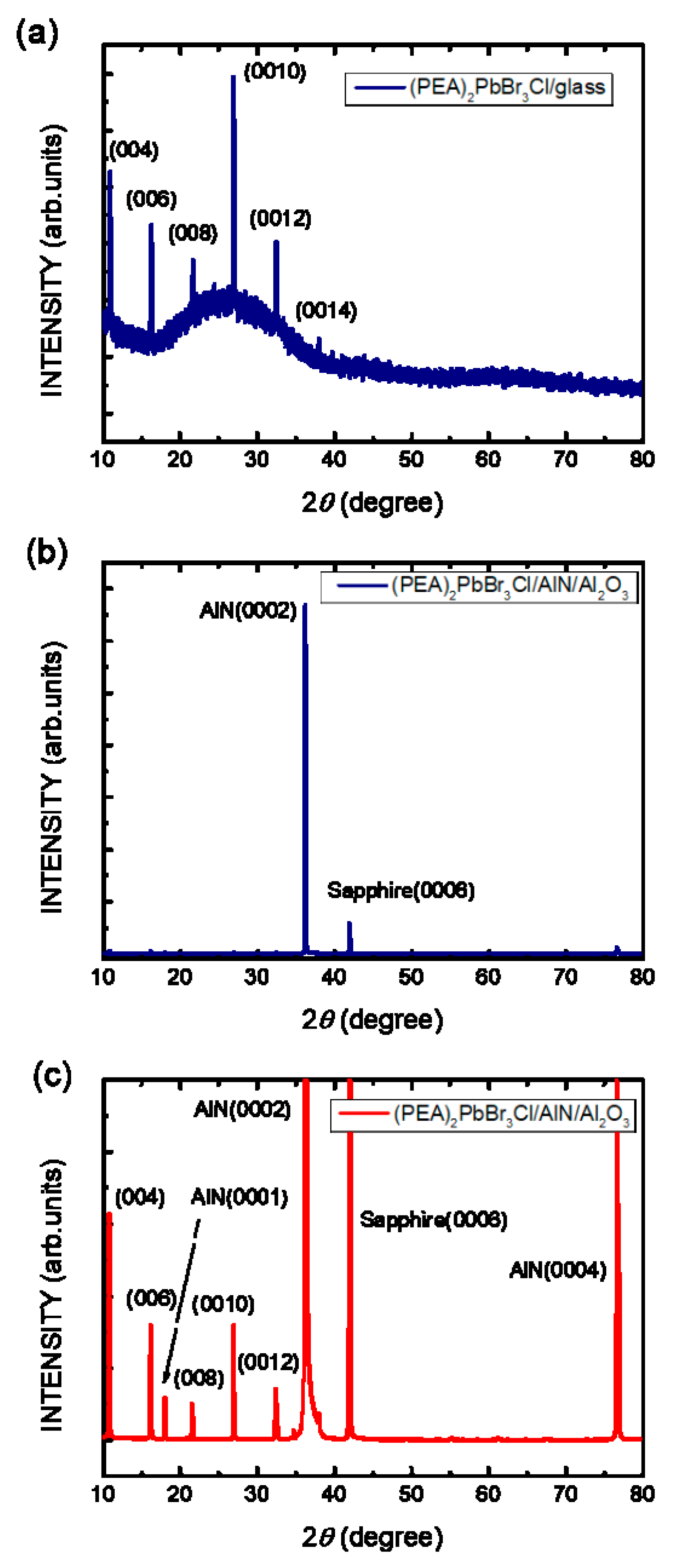
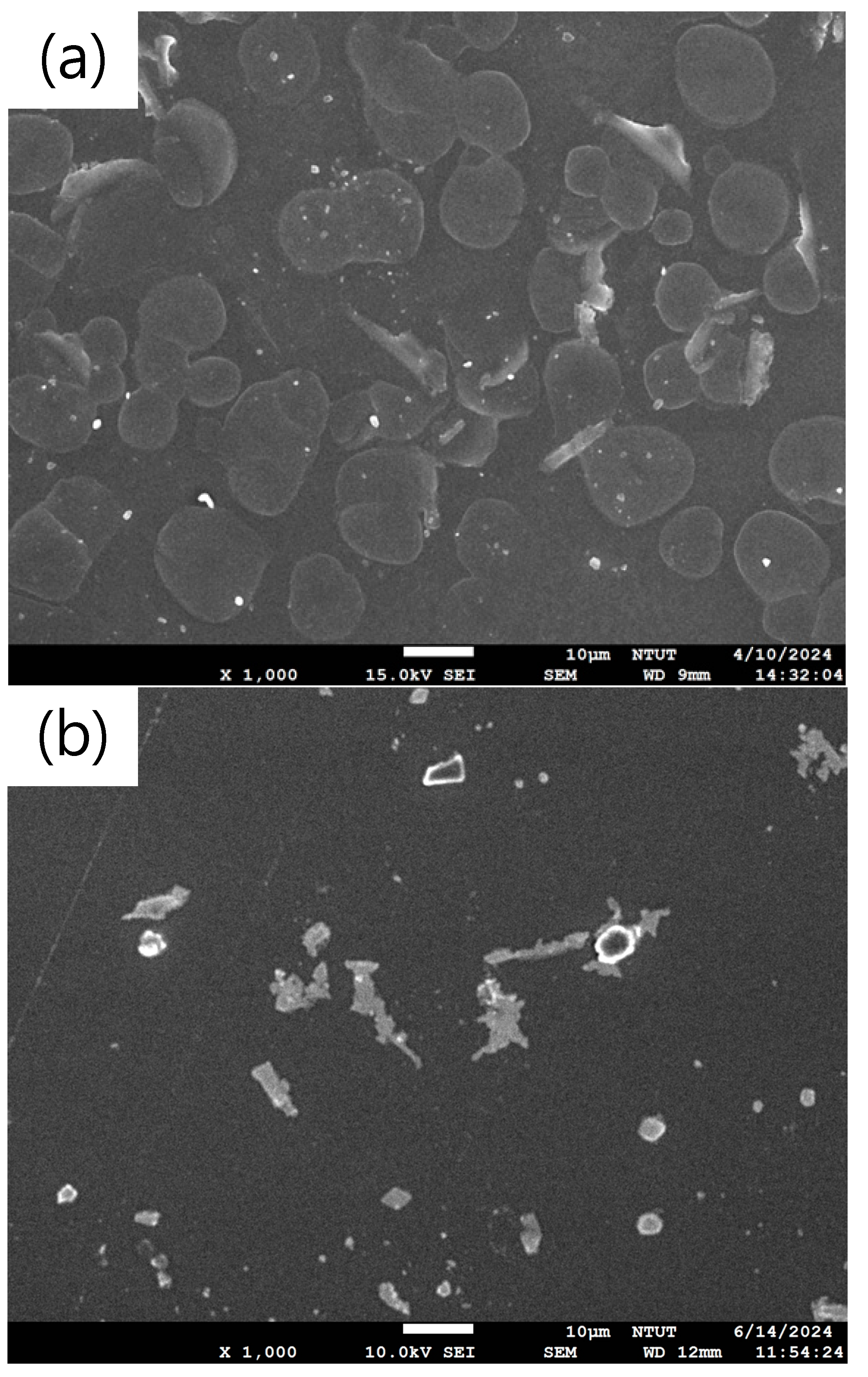
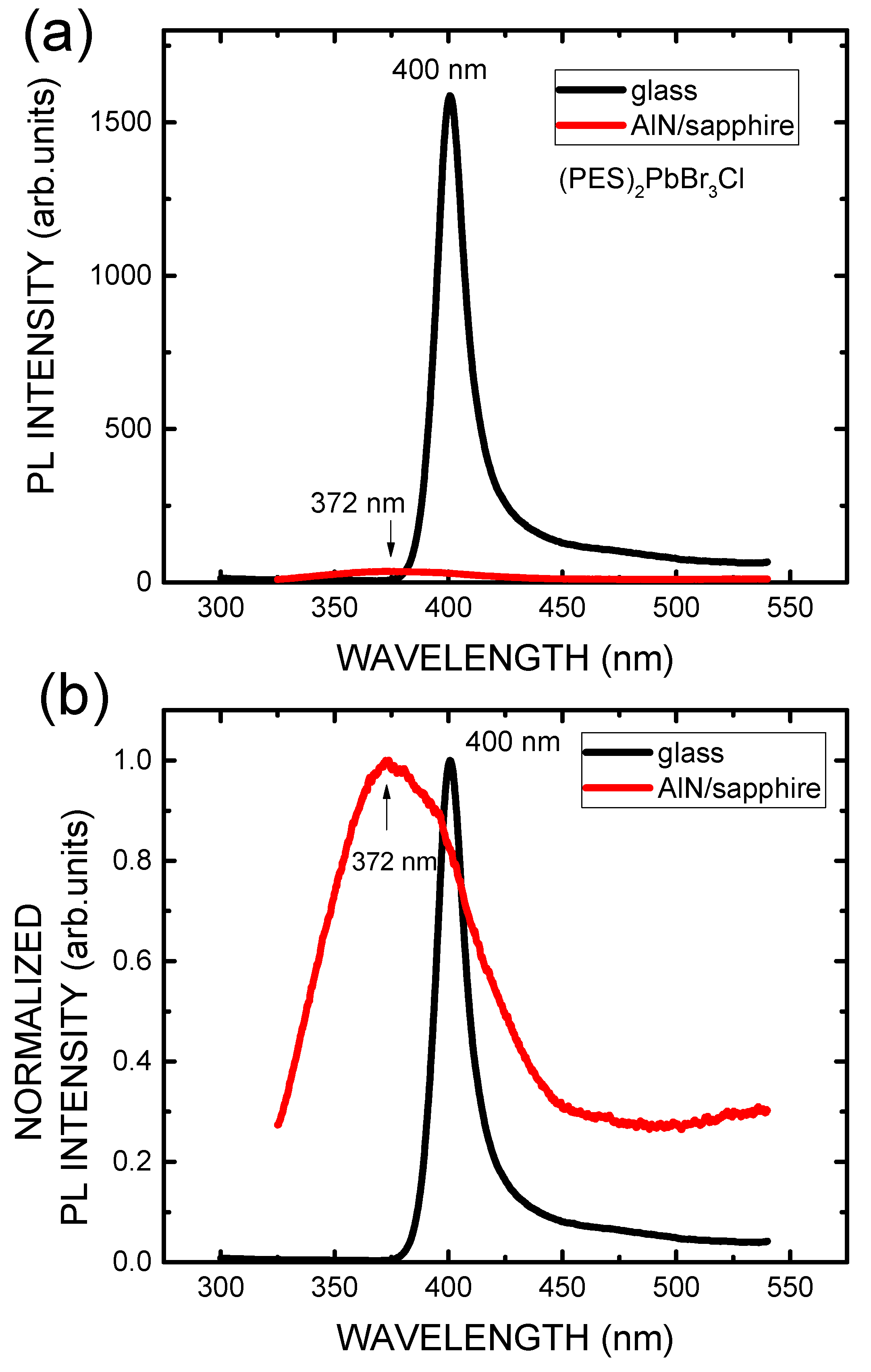
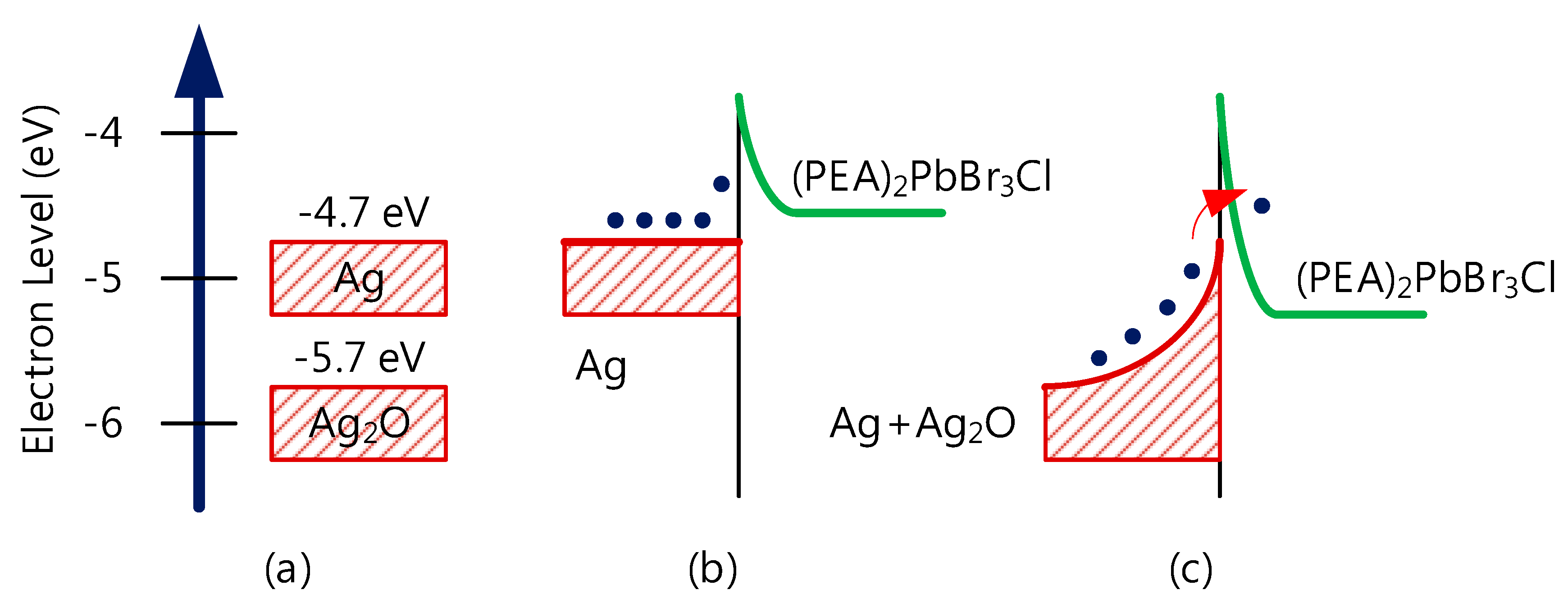
3. Results and Discussion

Figure 2a,b plot the XRD pattern of the (PEA)2PbBr3Cl perovskite on the glass substrate and AlN/sapphire substrate, respectively. Figure 2c shows the XRD pattern of Figure 2b with 7 times magnification. Six XRD spectra peaks of perovskite-like (PEA)2PbBr3Cl on the AlN/sapphire substrate and glass substrate were observed at around 10.83°, 16.15°, 21.50°, 26.90°, 32.38°, and 37.93°, corresponding to the (004), (006), (008), (0010), (0012), and (0014) phases of the quasi-2D (PEA)2PbBr3Cl structure, respectively [16,17]. The domain sizes D of the (PEA)2PbBr3Cl perovskite on the glass substrate and AlN/sapphire substrate were 50.7 and 17.1 nm, respectively, and were calculated using the Scherrer equation [18]. The crystallite size D of the (PEA)2PbBr3Cl film was
D = k λ β c o s θ
where k is the Scherrer constant, λ is the wavelength of the radiation (1.54 Å for the Cu target), and β and θ are the FWHM and Bragg angle of the (0010) phase, respectively. The degradation in crystal quality may have contributed to the preferred orientation of the (PEA)2PbBr3Cl perovskite, which was destroyed by the lattice of the AlN/sapphire substrate due to strained force.
Figure 3a,b show the top-view SEM image of the (PEA)2PbBr3Cl perovskite on AlN/sapphire without and with 300 °C annealing, respectively. The typical structure of (PEA)2PbBr3Cl perovskite is hexagonal [19]. For the pristine sample, oval- or round-shaped particles were observed on the surface of the (PEA)2PbBr3Cl perovskite film on the AlN/sapphire substrate. This may have been caused by the lattice mismatch during (PEA)2PbBr3Cl perovskite crystal growth (aggregation), thereby causing changes in the crystal shape. However, after annealing at 300 °C for 10 min, the structure of the (PEA)2PbBr3Cl perovskite crystal was destroyed, as shown in Figure 3b.
Figure 4a shows the photoluminescence (PL) spectra of the perovskite-like material (PEA)2PbBr3Cl on the glass substrate and AlN/sapphire substrate heterostructure, respectively. Figure 4b shows the normalized PL spectra of Figure 4a. The peak positions of PL spectra were 400 and 372 nm, with a full width at half maximum (FWHM) of 15 and 85 nm, respectively. It is well known that perovskite materials have excellent preferred-orientation crystallinity and defect allowance [20,21]. The PL spectrum of the (PEA)2PbBr3Cl showed a very narrow FWHM on the glass substrate and a broad FWHM on the AlN/sapphire substrate heterostructure, with the latter indicating degradation of the (PEA)2PbBr3Cl film crystal quality. A blue shift in the peak position of the (PEA)2PbBr3Cl film from 400 to 372 nm was observed, possibly due to the emissions of electron–hole recombination from the conduction band and valence band. The preferred-orientation growth was destroyed when the (PEA)2PbBr3Cl film was spin-coated onto the AlN/sapphire single-crystal substrate because the atoms of the crystal needed to fit the crystal lattice of the AlN epilayer, but lattice strain caused lattice mismatch, quality degradation, and bandgap widening [14].
Figure 5 plots the current–voltage (I-V) characteristics of Ag/(PEA)2PbBr3Cl on the AlN/sapphire substrate heterostructure under different annealing temperatures. AlN with a 6.2 eV wide bandgap is a III-nitride semiconductor. Therefore, its conductivity is very poor, and it is close to being an insulator. The ohmic contact on AlN presents a serious issue for future optoelectronic device applications [22,23]. Similarly, perovskite-like (PEA)2PbBr3Cl is a wide-bandgap material. According to the PL spectrum, the bandgap of the (PEA)2PbBr3Cl on the AlN/sapphire substrate should be 3.33 eV. Hence, in this study, we used the perovskite-like (PEA)2PbBr3Cl material as a buffer layer between the ohmic contact metal and AlN layer to reduce the metal contact resistance. As shown in Figure 5, the Ag/(PEA)2PbBr3Cl on the AlN layer was almost non-conductive. After annealing treatment at 150 and 300 °C for 10 min, the conductivity of Ag/(PEA)2PbBr3Cl on the AlN layer improved. The resistance of the applied voltage at 9.9 V decreased to 1.7 and 1.1 × 10¹⁰ Ω from 2.7 × 10¹⁰ Ω of the as-deposited film, respectively. The mechanism of conductivity increase is shown in Figure 6. The work function of the Ag metal and electron affinity of the (PEA)2PbBr3Cl perovskite layer were 4.7 and 3.65 eV, respectively. The work functions of Ag and Ag2O were 4.7 and 5.7 eV, respectively, as shown in Figure 6a. The transportation of an electron from Ag to the (PEA)2PbBr3Cl layer was difficult due to the 1.05 eV barrier, as shown in Figure 6b. Part of the Ag transformed into Ag2O after annealing due to processes occurring in the air environment and formed the Ag and Ag2O complex layer. This caused the Fermi level of the (PEA)2PbBr3Cl layer to lower because of the thermal equilibrium [24]. Therefore, the electron in the Ag contact layer could easily transfer to the (PEA)2PbBr3Cl layer via the thermionic-field emission (TFE) mechanism. The electrons in the Ag contact could acquire a small amount of energy, enabling them to penetrate the top of the potential barrier and reach the (PEA)2PbBr3Cl layer via the tunneling effect, such that the conductivity between the Ag contact and (PEA)2PbBr3Cl semiconductor layer improved, as shown in Figure 6c. Hence, the contact between the Ag and (PEA)2PbBr3Cl was not an ohmic contact but a non-blocking contact due to the narrow potential barrier for electrons and the possibility of tunneling.

4. Conclusions

In this study, we demonstrated the characteristics of (PEA)2PbBr3Cl on an AlN/sapphire substrate heterostructure. A quasi-2D structure was observed. Six XRD spectra peaks of perovskite-like (PEA)2PbBr3Cl on both the AlN/sapphire substrate and glass substrate were observed at around 10.83°, 16.15°, 21.50°, 26.90°, 32.38°, and 37.93°, corresponding to the (004), (006), (008), (0010), (0012), and (0014) phases of the quasi-2D (PEA)2PbBr3Cl structure, respectively. The peak position of photoluminescence (PL) of (PEA)2PbBr3Cl on the AlN/sapphire substrate heterostructure was 372 nm. The emission wavelength was lower than that of the traditional lead halide perovskite light-emitting diodes (typically 410 to 780 nm). This indicates the potential for application in UV perovskite light-emitting diodes. The conductivity between the Ag contact area and as-deposited (PEA)2PbBr3Cl on the AlN was almost non-conductive. However, after annealing treatment at 150 and 300 °C for 10 min, the conductivity of the Ag/(PEA)2PbBr3Cl structure on the AlN/sapphire substrate improved. The work function mechanism of Ag2O with 5.7 eV caused the Fermi level of the (PEA)2PbBr3Cl layer to lower because of the thermal equilibrium with Ag and Ag2O contacts after the annealing process, such that the electron in the Ag contact could easily transfer to the (PEA)2PbBr3Cl layer via the thermionic field emission (TFE) mechanism. Due to having higher stability than that of 3D perovskite materials, the two-dimensional, perovskite-like (PEA)2PbBr3Cl layer could be a candidate material for UV LEDs and AlN-based devices for ohmic contact and high-power devices.

Author Contributions

Conceptualization, Y.-H.L. and L.-C.C.; methodology, J.-S.N.; formal analysis, Y.-H.L. and L.-C.C.; resources, Y.-H.L. and L.-C.C.; data curation, J.-S.N.; writing—original draft preparation, Y.-H.L. and L.-C.C.; writing—review and editing, L.-C.C.; supervision, L.-C.C.; funding acquisition, L.-C.C. All authors have read and agreed to the published version of the manuscript.

Funding

This research was funded by the National Science and Technology Council of Taiwan, grant number 111-2221-E-027-040-MY3.

Institutional Review Board Statement

Not applicable.

Informed Consent Statement

Not applicable.

Data Availability Statement

The data presented in this study are available in the article.

Acknowledgments

This work was supported by the National Science and Technology Council of Taiwan (no. 111-2221-E-027-040-MY3).

Conflicts of Interest

The authors declare no conflicts of interest.

References

  1. Yu, J.C.; Park, J.H.; Lee, S.Y.; Song, M.H. Effect of perovskite film morphology on device performance of perovskite light-emitting diodes. Nanoscale 2019, 11, 1505–1514. [Google Scholar] [CrossRef]
  2. Lu, M.; Zhang, Y.; Wang, S.; Guo, J.; Yu, W.W.; Rogach, A.L. Metal halide perovskite light-emitting devices: Promising technology for next-generation displays. Adv. Funct. Mater. 2019, 29, 1902008. [Google Scholar] [CrossRef]
  3. Quan, L.N.; Rand, B.P.; Friend, R.H.; Mhaisalkar, S.G.; Lee, T.W.; Sargent, E.H. Perovskites for next-generation optical sources. Chem. Rev. 2019, 119, 7444–7477. [Google Scholar] [CrossRef]
  4. Hassan, Y.; Park, J.H.; Crawford, M.L.; Sadhanala, A.; Lee, J.; Sadighian, J.C.; Mosconi, E.; Shivanna, R.; Radicchi, E.; Jeong, M.; et al. Ligand-engineered bandgap stability in mixed-halide perovskite LEDs. Nature 2021, 591, 72–77. [Google Scholar] [CrossRef]
  5. Tan, Z.K.; Moghaddam, R.S.; Lai, M.L.; Docampo, P.; Higler, R.; Deschler, F.; Price, M.; Sadhanala, A.; Pazos, L.M.; Credgington, D.; et al. Bright light-emitting diodes based on organometal halide perovskite. Nat. Nanotechnol. 2014, 9, 687–692. [Google Scholar] [CrossRef]
  6. Bai, W.; Xuan, T.; Zhao, H.; Dong, H.; Cheng, X.; Wang, L.; Xie, R.J. Perovskite light-emitting diodes with an external quantum efficiency exceeding 30%. Adv. Mater. 2023, 35, 2302283. [Google Scholar] [CrossRef]
  7. Protesescu, L.; Yakunin, S.; Kumar, S.; Bär, J.; Bertolotti, F.; Masciocchi, N.; Guagliardi, A.; Grotevent, M.; Shorubalko, I.; Bodnarchuk, M.I.; et al. Dismantling the “Red Wall” of Colloidal Perovskites: Highly Luminescent Formamidinium and Formamidinium–Cesium Lead Iodide Nanocrystals. ACS Nano 2017, 11, 3119–3134. [Google Scholar] [CrossRef]
  8. Kovalenko, M.V.; Protesescu, L.; Bodnarchuk, M.I. Properties and potential optoelectronic applications of lead halide perovskite nanocrystals. Science 2017, 358, 745–750. [Google Scholar] [CrossRef]
  9. Yu, Y.; Tang, Y.; Wang, B.; Zhang, K.; Tang, J.X.; Li, Y.Q. Red Perovskite Light-Emitting Diodes: Recent Advances and Perspectives. Laser Photo. Rev. 2023, 17, 2200608. [Google Scholar] [CrossRef]
  10. Rahil, M.; Ansari, R.M.; Prakash, C.; Islam, S.S.; Dixit, A.; Ahmad, S. Ruddlesden–Popper 2D perovskites of type (C6H9C2H4NH3)2(CH3NH3)n−1PbnI3n+1 (n = 1–4) for optoelectronic applications. Sci. Rep. 2022, 12, 2176. [Google Scholar] [CrossRef]
  11. Chen, L.C.; Lee, K.L.; Wu, W.T.; Hsu, C.F.; Tseng, Z.L.; Sun, X.H.; Kao, Y.T. Effect of Different CH3NH3PbI3 Morphologies on Photovoltaic Properties of Perovskite Solar Cells. Nanoscale Res. Lett. 2018, 13, 140. [Google Scholar] [CrossRef]
  12. Mandal, S.; Khan, B.A.; Sarkar, P. 2D lead free Ruddlesden-Popper phase perovskites as efficient photovoltaic materials: A first-principles investigation. Comput. Mater. Sci. 2022, 211, 111545. [Google Scholar] [CrossRef]
  13. Chen, J.; Shi, Y.; He, Y.; Zhai, T. Two-dimensional Ruddlesden-Popper perovskite nanosheets: Synthesis, optoelectronic properties and miniaturized optoelectronic devices. FlatChem 2019, 17, 100116. [Google Scholar] [CrossRef]
  14. Chen, L.C.; Chen, C.C.; Chang, S.H.; Chen, S.H.; Kuo, H.C. Formation and characterization of preferred oriented perovskite thin films on single-crystalline substrates. Mater. Res. Express 2018, 5, 066403. [Google Scholar] [CrossRef]
  15. Hickman, A.L.; Chaudhuri, R.; Bader, S.J.; Nomoto, K.; Li, L.; Hwang, J.C.M.; Xing, H.G.; Jena, D. Next generation electronics on the ultrawide-bandgap aluminum nitride platform. Semicond. Sci. Technol. 2021, 36, 044001. [Google Scholar] [CrossRef]
  16. Zhang, X.; Shi, H.; Dai, H.; Zhang, X.; Sun, X.W.; Zhang, Z. Exciton-Polariton Properties in Planar Microcavity of Millimeter-Sized Two-Dimensional Perovskite Sheet. ACS Appl. Mater. Interfaces 2020, 12, 5081–5089. [Google Scholar] [CrossRef]
  17. Wu, S.C.; Wu, C.S.; Chien, C.H.; Zhang, Y.W.; Yang, C.X.; Liu, C.; Li, M.H.; Lin, C.F.; Wu, Y.H.; Lin, B.H.; et al. Carrier–Phonon Interaction Induced Large Negative Thermal-Optic Coefficient at Near Band Edge of Quasi-2D (PEA)2PbBr4 Perovskite. Adv. Funct. Mater. 2023, 33, 2213427. [Google Scholar] [CrossRef]
  18. Chen, L.C.; Wei, Y.S.; Zhang, M. Double buffer of MAPbBr3 QDs using a bulk crystal source by the LARP method and MABr modifier for CsPbBr3 perovskite light-emitting diodes. J. Phys. D Appl. Phys. 2023, 56, 465102. [Google Scholar] [CrossRef]
  19. Ge, C.; Zhai, W.; Tain, C.; Zhao, S.; Guo, T.; Sun, S.; Chen, W.; Ran, G. Centimeter-scale 2D perovskite (PEA)2PbBr4 single crystal plates grown by a seeded solution method for photodetectors. RSC Adv. 2019, 9, 16779–16783. [Google Scholar] [CrossRef]
  20. Wang, F.; Bai, S.; Tress, W.; Hagfeldt, A.; Gao, F. Defects engineering for high-performance perovskite solar cells. npj Flexible Electron. 2018, 2, 22. [Google Scholar] [CrossRef]
  21. Li, B.; Shen, T.; Yun, S. Recent progress of crystal orientation engineering in halide perovskite photovoltaics. Mater. Horiz. 2023, 10, 13–40. [Google Scholar] [CrossRef] [PubMed]
  22. Abid, I.; Mehta, J.; Cordier, Y.; Derluyn, J.; Degroote, S.; Miyake, H.; Medjdoub, F. AlGaN Channel High Electron Mobility Transistors with Regrown Ohmic Contacts. Electronics 2021, 10, 635. [Google Scholar] [CrossRef]
  23. Yang, L.; Wang, J.; Sheng, S.; Zhang, B.; Sheng, B.; Wang, T.; Liu, F.; Tao, R.; Xu, F.; Yang, X.; et al. Low-Resistive Ohmic Contacts in High-Electron-Mobility AlN/GaN Heterostructures by Suppressing the Oxygen Incorporation. ACS Appl. Electron. Mater. 2022, 4, 3632–3639. [Google Scholar] [CrossRef]
  24. Magari, Y.; Makino, H.; Hashimoto, S.; Furuta, M. Origin of work function engineering of silver oxide for an In–Ga–Zn–O Schottky diode. Appl. Sur. Sci. 2020, 512, 144519. [Google Scholar] [CrossRef]
Figure 1. Structure of the perovskite-like (PEA)2PbBr3Cl on the AlN/sapphire substrate heterostructure.
Applsci 14 06096 g001
Figure 2. XRD pattern of the (PEA)2PbBr3Cl perovskite on (a) glass and (b) AlN/sapphire. (c) XRD pattern of (b) with 7 times magnification.
Applsci 14 06096 g002
Figure 3. Top-view SEM image of the (PEA)2PbBr3Cl perovskite on AlN/sapphire (a) without and (b) with 300 °C annealing.
Applsci 14 06096 g003
Figure 4. (a) Photoluminescence (PL) and (b) normalized PL spectra of the perovskite-like (PEA)2PbBr3Cl material on glass and AlN/sapphire substrate heterostructure, respectively.
Applsci 14 06096 g004
Figure 5. Current-voltage (I-V) characteristics of Ag/(PEA)2PbBr3Cl on AlN/sapphire substrate heterostructure.
Applsci 14 06096 g005
Figure 6. (a) Schematic energy level diagram of Ag and Ag2O and their contact area with (PEA)2PbBr3Cl (b) before and (c) after annealing.
Applsci 14 06096 g006
Disclaimer/Publisher’s Note: The statements, opinions and data contained in all publications are solely those of the individual author(s) and contributor(s) and not of MDPI and/or the editor(s). MDPI and/or the editor(s) disclaim responsibility for any injury to people or property resulting from any ideas, methods, instructions or products referred to in the content.

