
Mitigating the Impact of Asymmetric Deformation on Advanced Metrology for Photolithography

Abstract
1. Introduction
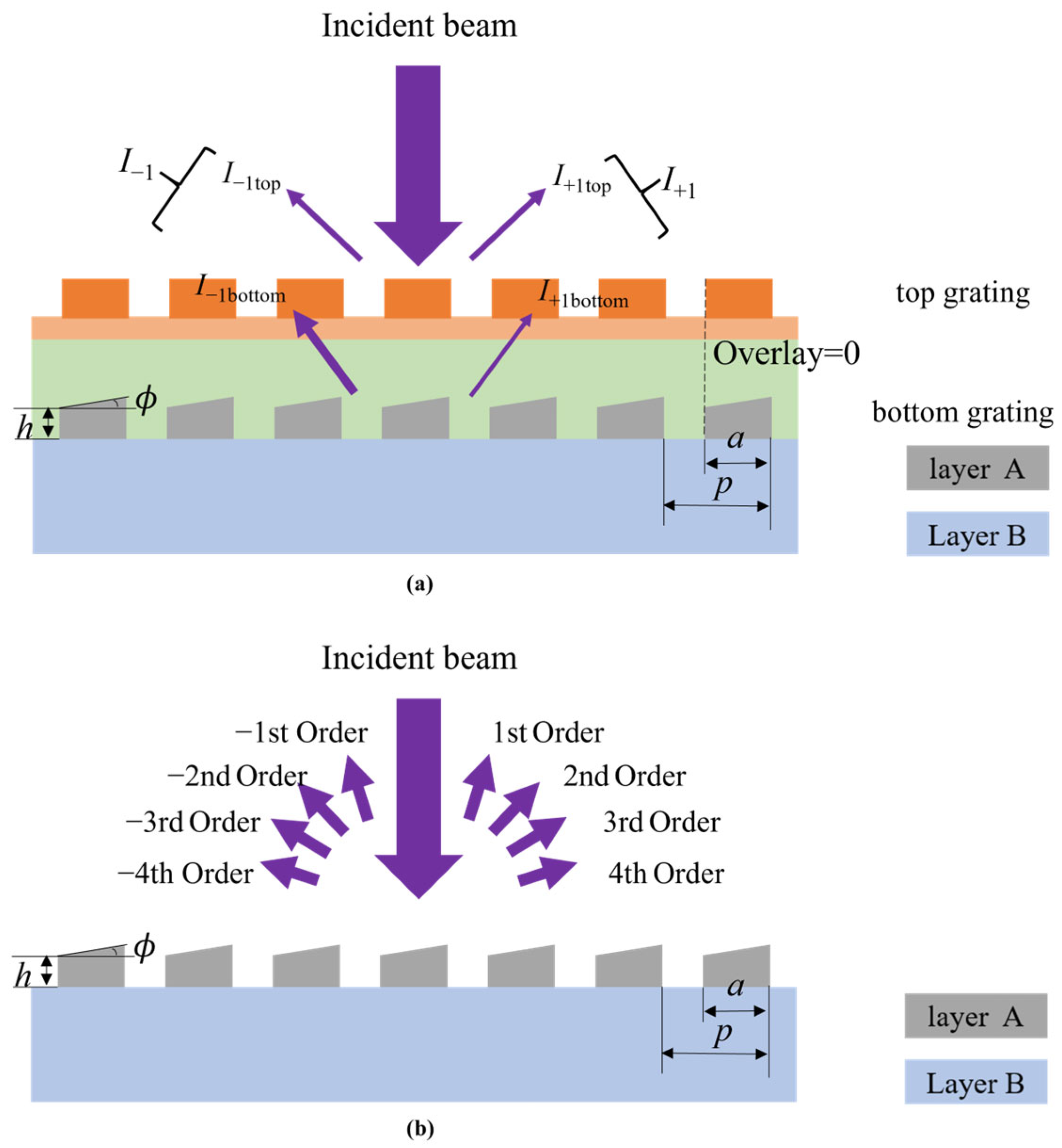
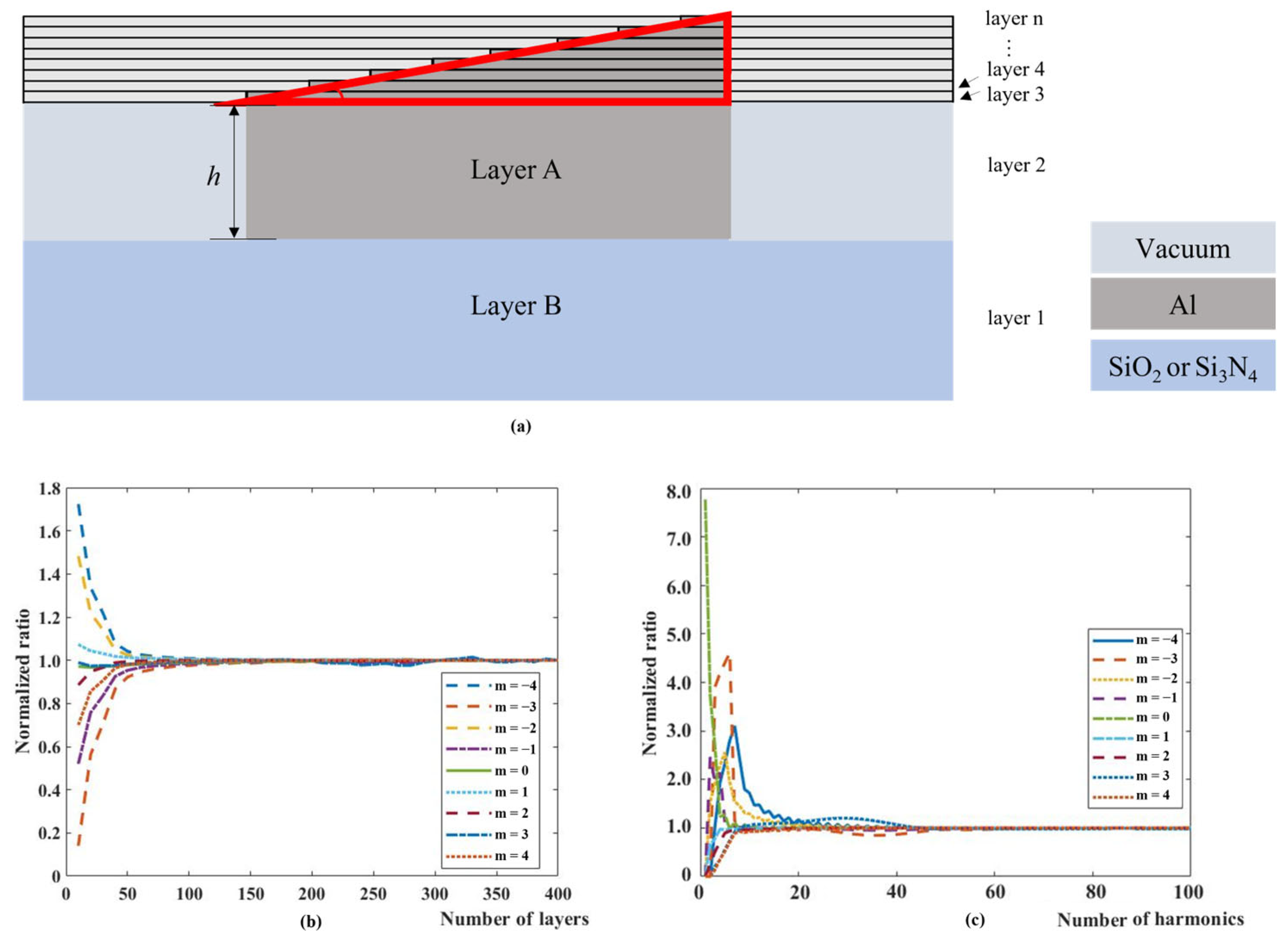
2. Model Creation
3. Results and Discussion
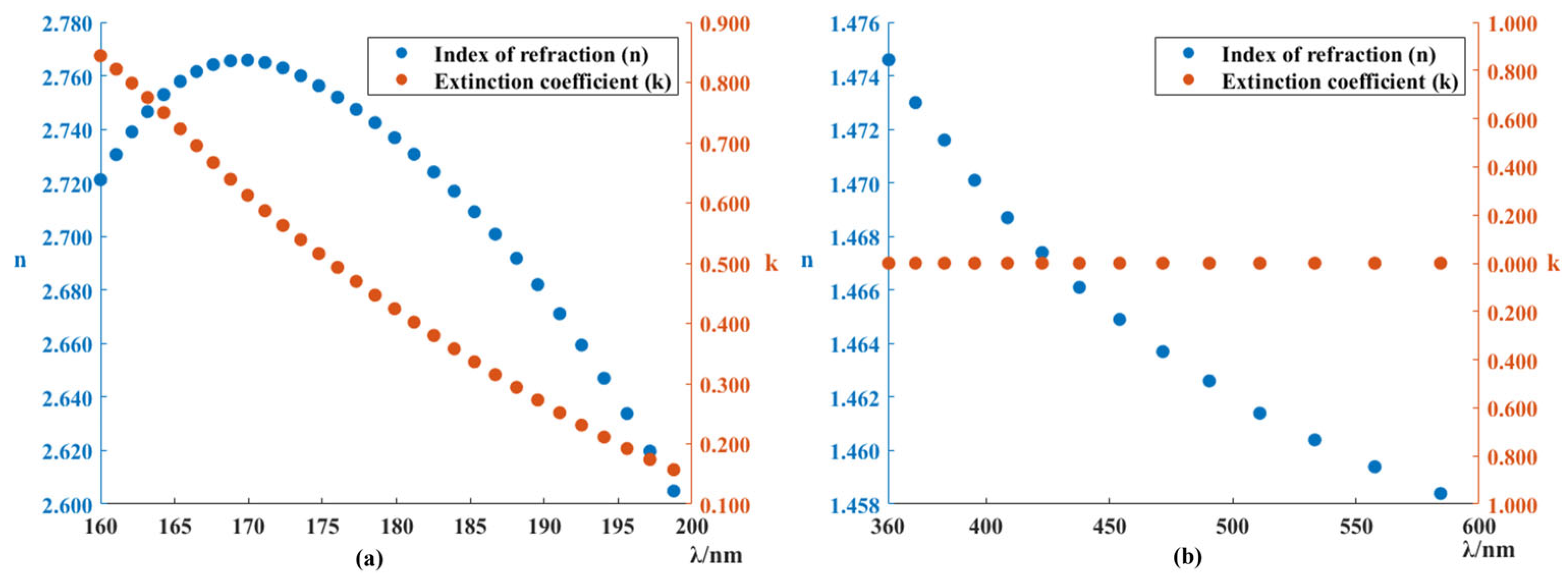
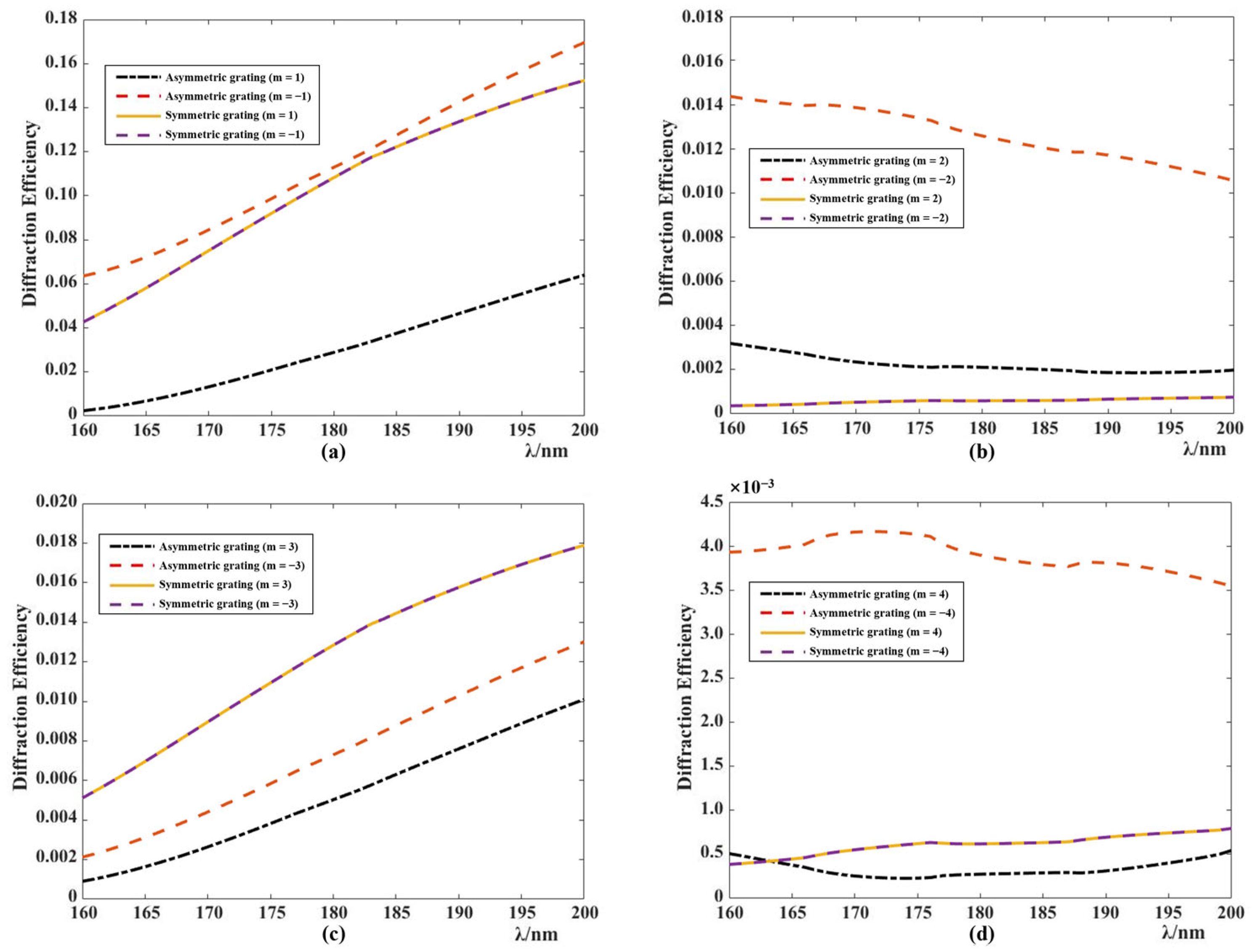
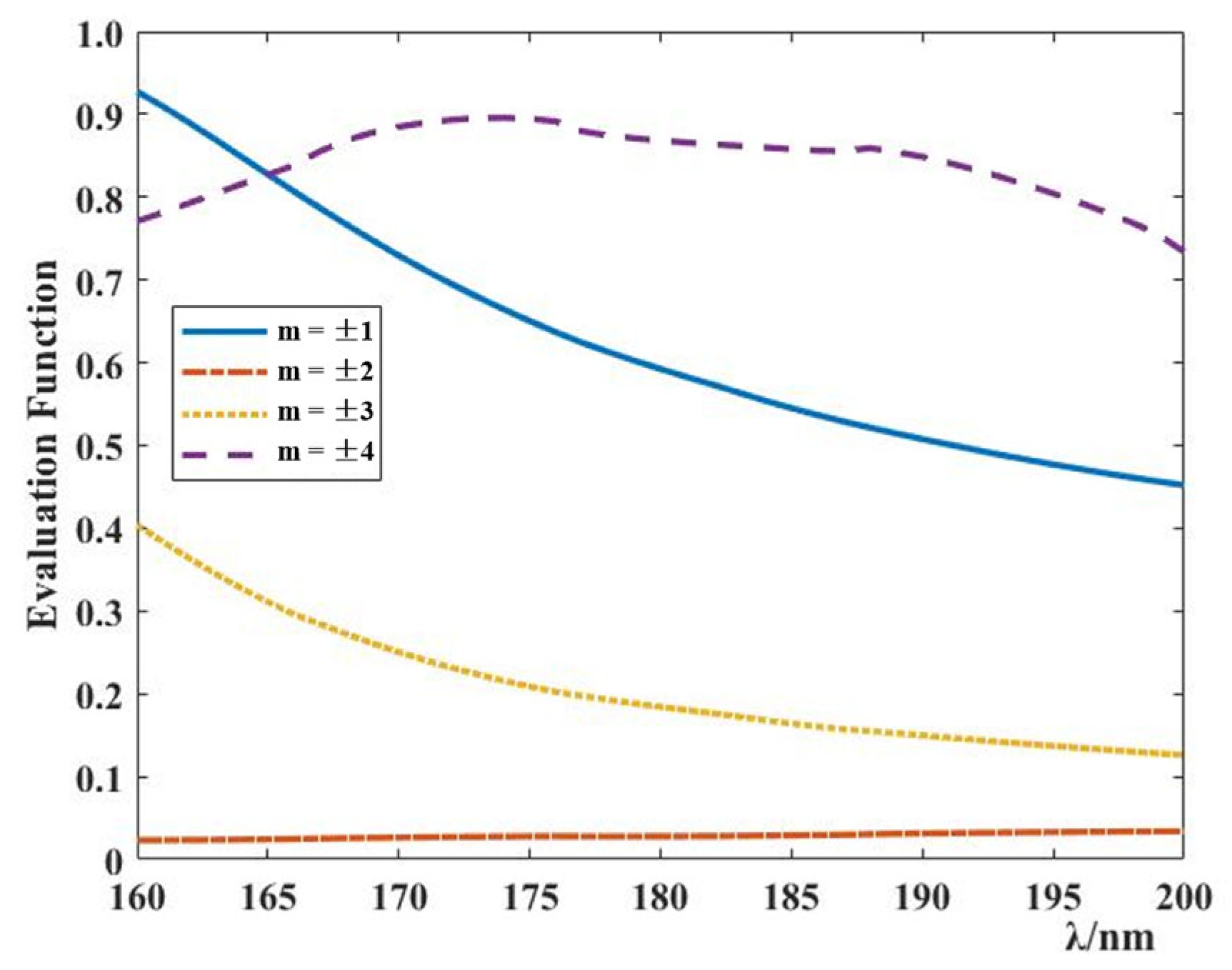
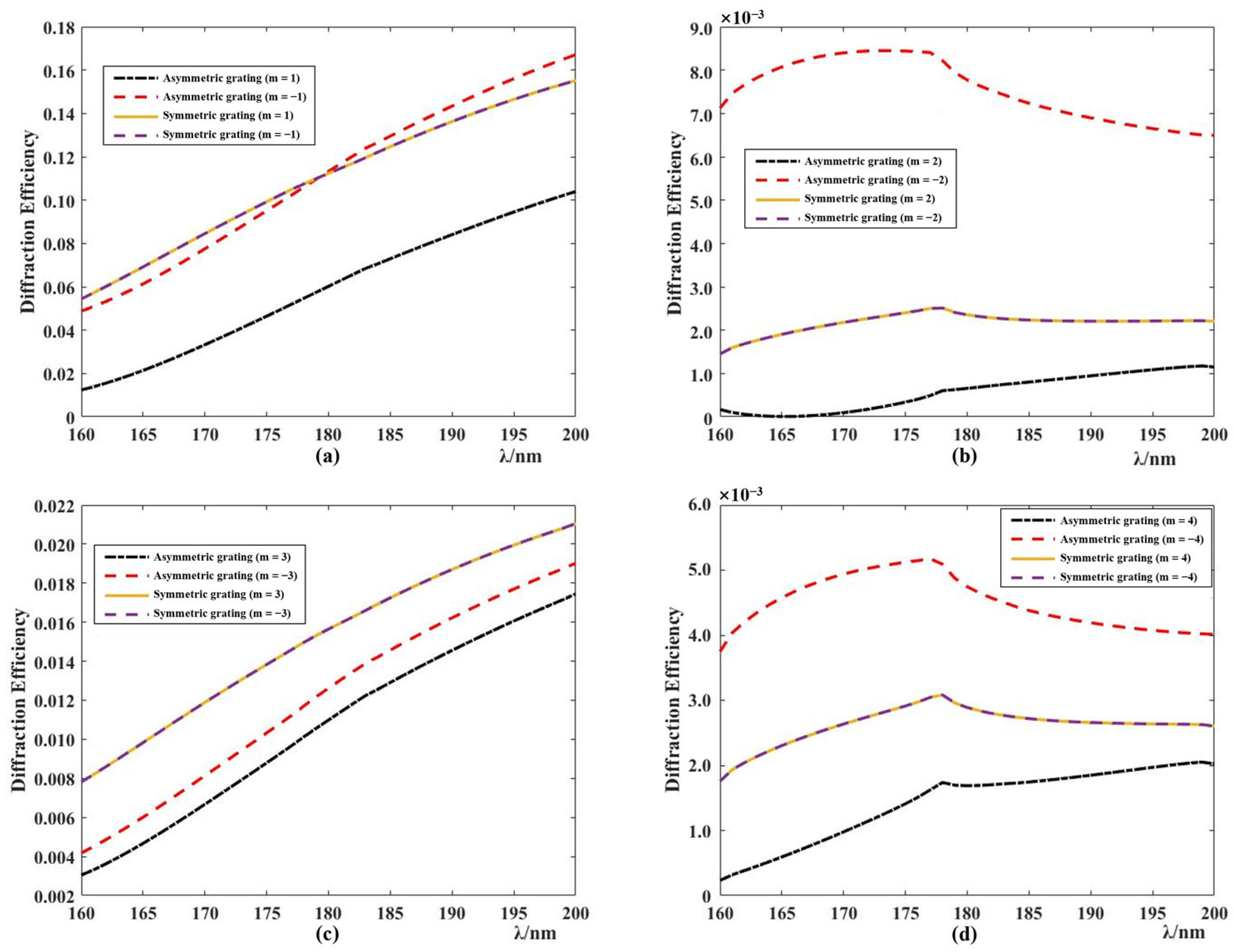
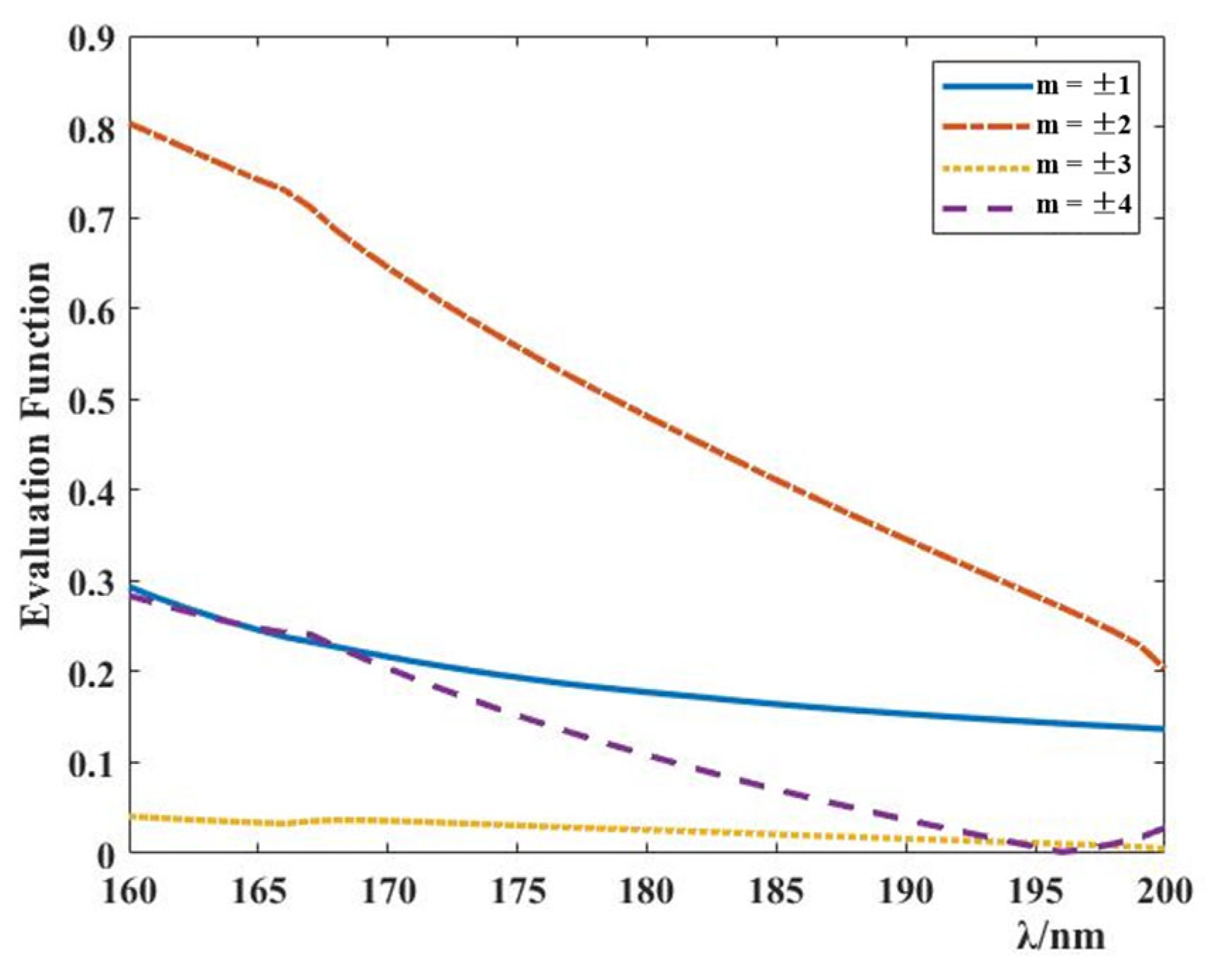
3.1. Material System 1 (Layer A: Al, and Layer B: Si3N4)
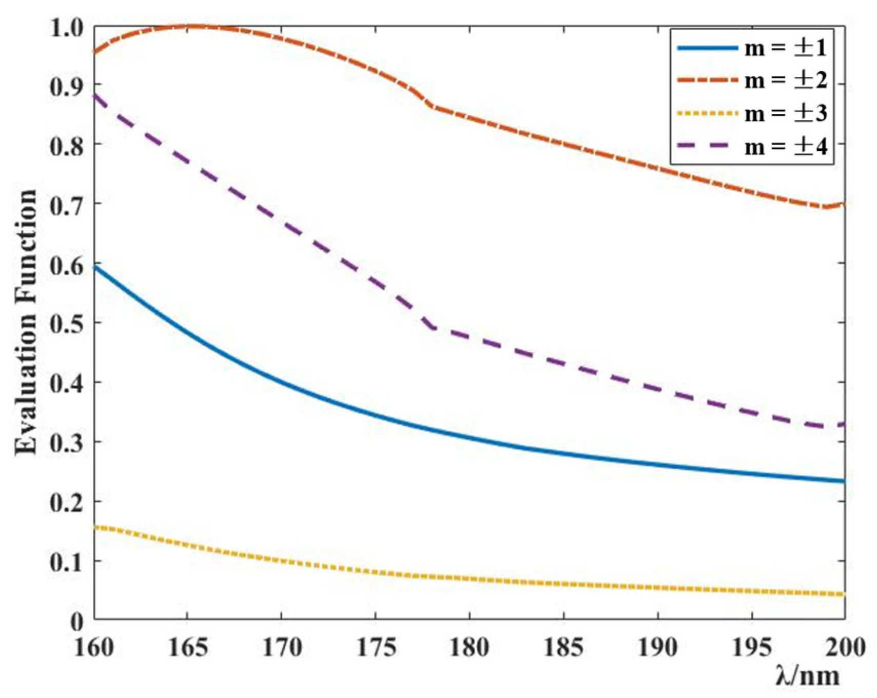
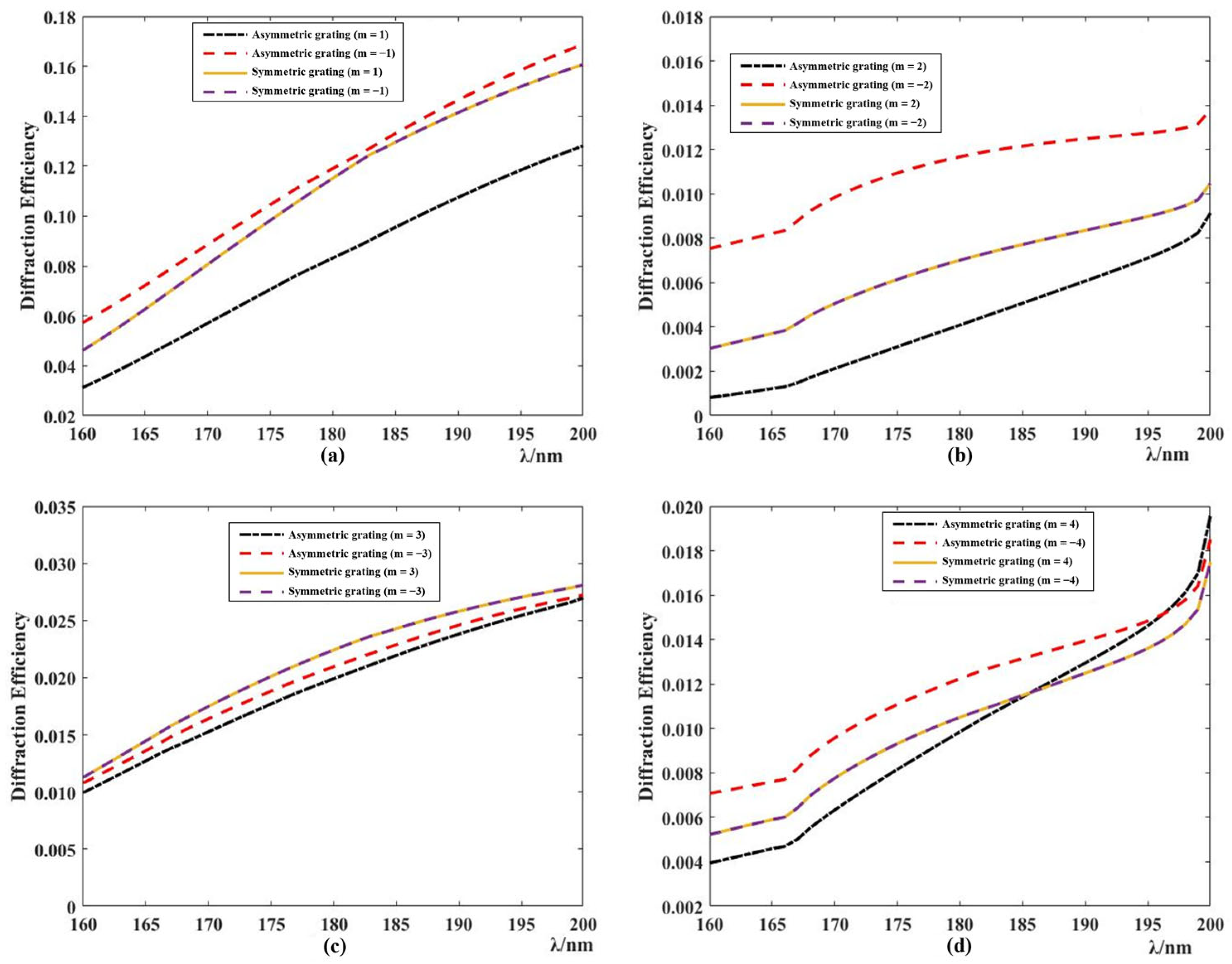
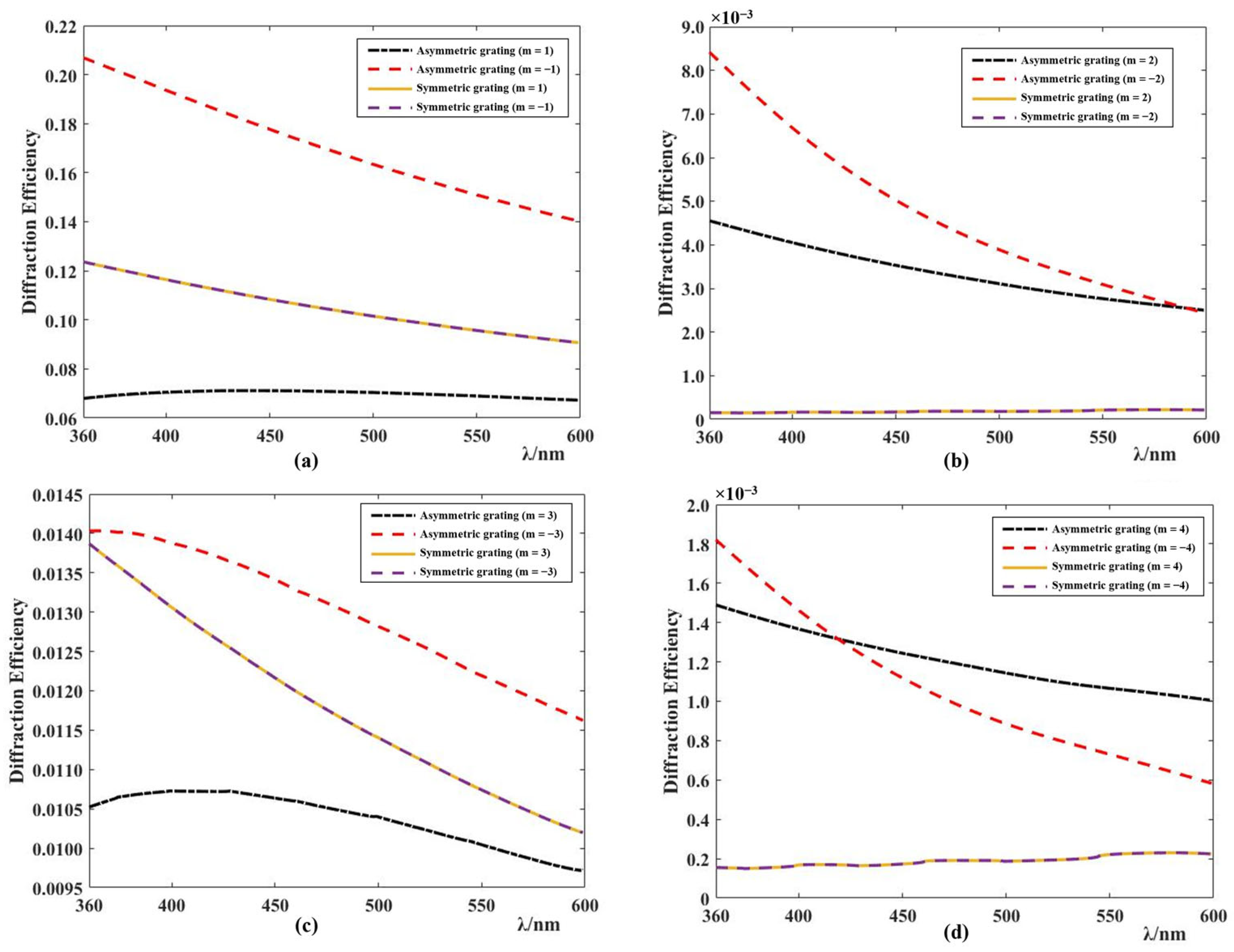
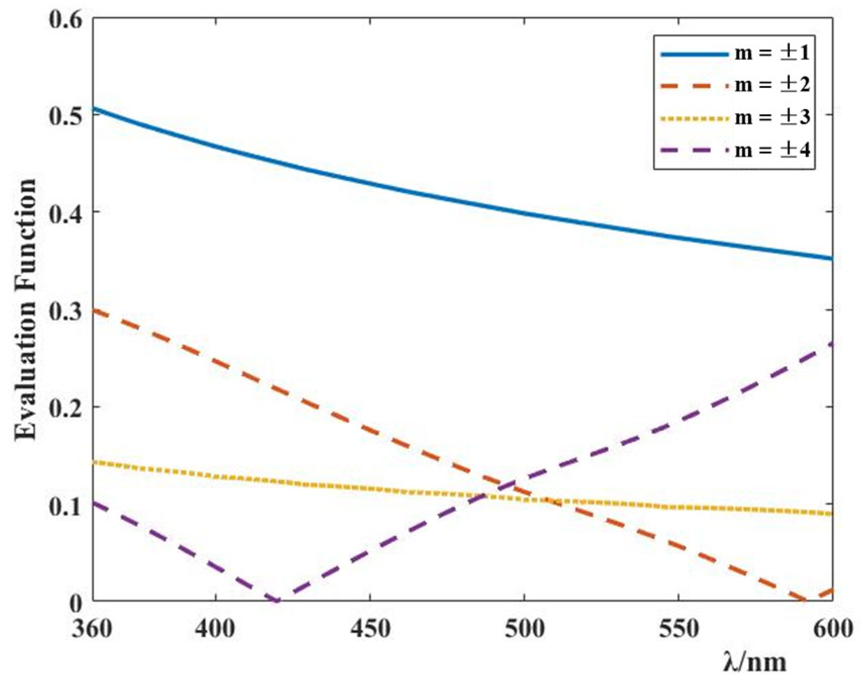
3.2. Material System 2 (Layer A: Al, and Layer B: SiO2)
3.3. Summary of the Material Systems
4. Conclusions
Author Contributions
Funding
Institutional Review Board Statement
Informed Consent Statement
Data Availability Statement
Conflicts of Interest
References
- Wischmeier, L.; Graeupner, P.; Kuerz, P.; Kaiser, W.; van Schoot, J.; Mallmann, J.; de Pee, J.; Stoeldraijer, J. High-NA EUV lithography optics becomes reality. Proc. SPIE 2020, 11323, 1132308. [Google Scholar]
- Ngo, A.; Dey, B.; Halder, S.; Gendt, S. Machine learning-based edge placement error analysis and optimization: A systematic review. IEEE Trans. Semicond. Manuf. 2023, 36, 1–13. [Google Scholar] [CrossRef]
- Macka, C.A.; Adelb, M.E. Overlay and edge placement error metrology in the era of stochastics. Proc. SPIE 2023, 12496, 1249609. [Google Scholar]
- Slotboom, D.M.; Hinnen, P.; Mulkens, J. On-product overlay solutions for DUV and EUV mix-scanner usage in an EPE-driven patterning world. Proc. SPIE 2022, 12051, 120510L. [Google Scholar]
- Mulkens, J.; Slachter, B.; Kubis, M.; Tel, W.; Hinnen, P.; Maslow, M.; Dillen, H.; Ma, E.; Chou, K.; Liu, X.; et al. Holistic approach for overlay and edge placement error to meet the 5nm technology node requirements. Proc. SPIE 2018, 10585, 105851L. [Google Scholar]
- Bhattacharyya, K. Tough road ahead for device overlay and edge placement error. Proc. SPIE 2019, 10959, 1095902. [Google Scholar]
- Jee, T.; You, J.; Lee, H.; Lee, S.; Hong, S.; Seo, J.; Meir, R.; Oved, N.; Park, J.; Kim, S.; et al. Budgeting and predicting pattern defects using edge placement error and machine learning. In Proceedings of the 2023 7th IEEE Electron Devices Technology & Manufacturing Conference (EDTM), Seoul, Republic of Korea, 7–10 March 2023. [Google Scholar]
- Shchegrov, A.; Leray, P.; Paskover, Y.; Yerushalmi, L.; Megged, E.; Grauer, Y.; Gronheid, R. On product overlay metrology challenges in advanced nodes. Proc. SPIE 2020, 11325, 113251P. [Google Scholar]
- Jin, H.; Qi, Y. Review of overlay error and controlling methods in alignment system for advanced lithography. Proc. SPIE 2022, 12478, 1247843. [Google Scholar]
- Zhang, J.; Chen, X.; Yang, T.; Liu, S. X-ray-based overlay metrology using reciprocal space slicing analysis. Opt. Lett. 2023, 48, 6380–6383. [Google Scholar] [CrossRef]
- Park, D.; Kim, H.; Seo, M.; Ju, J.; Kim, Y.; Shahrjerdy, M.; Leest, A.; Soco, A.; Miceli, G.; Massier, J.; et al. Unique method for controlling device level overlay with high-NA optical overlay technique using YieldStar in a DRAM HVM environment. Proc. SPIE 2018, 10585, 105850V. [Google Scholar]
- Koonmen, J. Applications products and business opportunity. In ASML Small Talk; ASML: Veldhoven, The Netherlands, 2021. [Google Scholar]
- Su, C.; Lin, Z.; Lin, Y.; Kuo, H. Enhancement of diffraction-based overlay model for overlay target with asymmetric sidewall. IEEE Trans. Semicond. Manuf. 2020, 33, 373–382. [Google Scholar] [CrossRef]
- Li, R.; Hsu, I.; Brożek, T.; Yang, L.; He, D.; Wu, F.; Ren, J.; Zhu, Y.; Zhang, Y.; Liu, P.; et al. In-line monitoring of overlay and process window using design-assisted voltage contrast inspection for 14 nm FINFET technology. Proc. SPIE 2022, 12053, 120531U. [Google Scholar]
- Shchegrov, A.; Leray, P.; Passover, Y.; Yerushalmi, L.; Megged, E.; Grauer, Y.; Gronheid, R. Optical overlay metrology trends in advanced nodes. Proc. SPIE 2022, 12053, 120530N. [Google Scholar]
- Eyring, S.; Selvanathan, D.; Blanton, W.; Shuall, N.; Laske, F. Multi-layer, any-shape on-device overlay metrology. Proc. SPIE 2022, PC12053, PC120530P. [Google Scholar]
- Lee, H.; Chang, H.; Shin, H.; Choi, O. Image-based overlay target design using a grating intersection. J. Micro/Nanopatterning Mater. Metrol. 2022, 21, 034801. [Google Scholar] [CrossRef]
- Blancquaert, Y.; Dezauzier, C. Diffraction based overlay and image based overlay on production flow for advanced technology node. Proc. SPIE 2013, 8681, 86812O. [Google Scholar]
- Dasari, P.; Li, J.; Hu, J.; Smith, N.; Kritsun, O. Diffraction-based overlay metrology for double patterning technologies. Proc. SPIE 2009, 7272, 727212. [Google Scholar]
- Mathijssen, S.; Davis, T.; Boef, A.; Bhattacharyya, K. Fundamental understanding of the interplay between target and sensor brings diffraction based overlay to the next level of accuracy. Proc. SPIE 2021, 11611, 1161121. [Google Scholar]
- Matsunobu, M.; Nishiyama, T.; Inoue, M.; Housley, R.; Bozdog, C.; Lim, J.; Watson, B.; Reece, J.; McCandless, S.; Zwier, O.; et al. Novel diffraction-based overlay metrology utilizing phase-based overlay for improved robustness. Proc. SPIE 2021, 11611, 1161126. [Google Scholar]
- Hsieh, H.; Cheng, J.; Yeh, Y. Optimized wavelength selection for diffraction-based overlay measurement by minimum asymmetry factor variation with finite-difference time-domain simulation. Appl. Opt. 2022, 61, 1389–1397. [Google Scholar] [CrossRef]
- Bian, Y.; Guan, X.; Liu, B.; Guo, X.; Zhang, C.; Zhou, W.; Huang, J.; Zhang, Y.; Guo, L.; Liu, F.; et al. A study of overlay accuracy improvement on process induced asymmetry effect. In Proceedings of the 2021 International Workshop on Advanced Patterning Solutions (IWAPS), Foshan, China, 12–13 December 2021. [Google Scholar]
- Li, Y.; Wei, Y.; Wu, Q.; Liu, X.; Wang, Q. A study of diffraction-based overlay (DBO) on a 3 nm CFET metal layer. Proc. SPIE 2023, 12496, 124962Y. [Google Scholar]
- Xu, B.; Wu, Q.; Chen, R.; Dong, L.; Zhang, L.; Wei, Y. A study on diffraction-based overlay measurement based on FDTD method. Proc. SPIE 2021, 11611, 116113B. [Google Scholar]
- Hinnen, P. YieldStar Metrology System Applications for Advanced Process Control; ASML: Veldhoven, The Netherlands; IMEC: Leuven, Belgium, 2018. [Google Scholar]
- Mohamad, H.; Essaidi, S.; Blaize, S.; Macias, D.; Benech, P.; Morand, A. Fast Fourier factorization for differential method and RCWA: A powerful tool for the modeling of non-lamellar metallic diffraction gratings. Opt. Quant. Electron. 2020, 52, 127. [Google Scholar] [CrossRef]
- GSolver. Diffraction Grating Analysis for Windows. Available online: https://gsolver.com/ (accessed on 8 March 2024).


| Wavelength/nm | Pitch/nm | The Optimal Diffraction Order |
|---|---|---|
| Layer A: Al and Layer B: Si3N4 | ||
| 160–200 | 3000 | ±2nd |
| 160–200 | 1600 | ±3rd |
| 160–200 | 1200 | ±3rd |
| 160–200 | 600–1000 (step size: 100 nm) | ±3rd |
| Layer A: Al, and Layer B: SiO2 | ||
| 360–486 | 6000 | ±4th |
| 487–507 | 6000 | ±3rd |
| 508–600 | 6000 | ±2nd |
Disclaimer/Publisher’s Note: The statements, opinions and data contained in all publications are solely those of the individual author(s) and contributor(s) and not of MDPI and/or the editor(s). MDPI and/or the editor(s) disclaim responsibility for any injury to people or property resulting from any ideas, methods, instructions or products referred to in the content. |
© 2024 by the authors. Licensee MDPI, Basel, Switzerland. This article is an open access article distributed under the terms and conditions of the Creative Commons Attribution (CC BY) license (https://creativecommons.org/licenses/by/4.0/).
Share and Cite
Yang, W.; Yao, S.; Cao, J.; Lin, N. Mitigating the Impact of Asymmetric Deformation on Advanced Metrology for Photolithography. Appl. Sci. 2024, 14, 4440. https://doi.org/10.3390/app14114440
Yang W, Yao S, Cao J, Lin N. Mitigating the Impact of Asymmetric Deformation on Advanced Metrology for Photolithography. Applied Sciences. 2024; 14(11):4440. https://doi.org/10.3390/app14114440
Chicago/Turabian StyleYang, Wenhe, Shuxin Yao, Jing Cao, and Nan Lin. 2024. "Mitigating the Impact of Asymmetric Deformation on Advanced Metrology for Photolithography" Applied Sciences 14, no. 11: 4440. https://doi.org/10.3390/app14114440
APA StyleYang, W., Yao, S., Cao, J., & Lin, N. (2024). Mitigating the Impact of Asymmetric Deformation on Advanced Metrology for Photolithography. Applied Sciences, 14(11), 4440. https://doi.org/10.3390/app14114440