Abstract
This study examines the effects of varying argon (Ar) and carbon tetrafluoride (CF4) gas flow rates on the etching of monocrystalline silicon substrates using surface discharge plasma. While previous research has primarily focused on the fundamental characteristics and applications of surface discharge plasma in silicon etching, the influence of the gas flow rate on etching efficacy remains insufficiently explored. The aim of this study is to elucidate the relationship between mixed gas flow rates and the rate and quality of silicon etching, both of which are critical for optimizing manufacturing processes in the semiconductor industry. Utilizing a setup equipped with a USB4000 spectrometer for emission spectroscopy, we varied the Ar/CF4 flow rates from 0 to 6000 sccm while maintaining a fixed discharge-sustaining voltage of 9.4 kV. We observed and analyzed the discharge power, plasma emission intensities, and resulting etch profiles of the silicon substrates. Particularly, we analyzed the emission spectra for peaks corresponding to active species such as F, F2, and CFn, indicative of the plasma’s etching capabilities. The findings revealed that higher flow rates significantly enhanced the generation of key active species, leading to increased etching rates in both depth and width directions of the silicon substrates. Importantly, an increase in flow rate also facilitated the diffusion of these species across a broader area, thereby advancing the etching process and inhibiting the deposition of etching byproducts. These results underscore the importance of optimizing gas flow rates to enhance etching efficiency and quality. In conclusion, this study confirms that adjusting the flow rates of Ar and CF4 in surface discharge plasma etching can significantly influence the effectiveness of the silicon etching process. This outcome will contribute to the realization and development of semiconductor etching technology, such as solar cell manufacturing, as well as the further advancement of atmospheric pressure non-equilibrium plasma surface treatment technology.
1. Introduction
In recent years, significant strides have been made in technology concerning the generation of glow discharge characterized by high spatial uniformity under atmospheric pressure conditions [1,2,3]. This technological breakthrough has practical applications as a surface treatment method for various materials, including semiconductors [4,5,6]. Etching stands out as one of the most crucial techniques for fabricating microelectronics [7,8]. Additionally, maskless etching technology for microelectronics is desirable due to its potential for low-cost fabrication. Traditionally, generating non-equilibrium plasma for atmospheric pressure pattern processing required conditions below atmospheric pressure. Furthermore, plasma processing within a pattern involved the sequential application and removal of a resist mask, which complicated the process. The authors explored the utilization plasma characteristics for spatial confinement under atmospheric pressure. Surface discharge plasma, known for its adaptable spatial distribution, enables the realization of maskless plasma pattern treatments [9,10]. The proposed surface discharge plasma technique allows the creation of non-equilibrium plasma within atmospheric pressure confines. Moreover, by confining the plasma within specific regions, patterned plasma etching can be carried out without relying on masking procedures. This advancement holds promise for applications in electrode grooving technology, particularly in the context of single-crystal silicon solar cells featuring buried contacts and selective emitter structure configurations [11,12,13]. Furthermore, the authors investigated the influence of argon (Ar) and carbon tetrafluoride (CF4) mixed gas flow rates on the formation of electrode grooves atop single-crystalline silicon substrates using surface discharge plasma [10]. However, these single-crystalline silicon substrates are additionally endowed with an anti-reflection film (SiₓNᵧ) and a textured structure achieved via wet processing [14,15,16]. The effect of the gas flow rate on the etching of silicon materials by surface discharge plasma etching must be evaluated using a silicon substrate with a flat surface. Optimizing the conditions for generating plasma and understanding the etching characteristics of silicon materials are crucial for verifying the potential for further applications of surface discharge plasma, not only in solar cell electrode groove fabrication but also in semiconductor manufacturing technology.
This study investigates the etching characteristics of flat-surface single-crystalline silicon substrates using surface discharge plasma generated under various Ar and CF4 mixed gas flow rate conditions. Consequently, we elucidate the influence of the Ar and CF4 mixed gas flow rate on the etching characteristics of single-crystalline silicon substrates.
2. Experimental Methods
Figure 1 illustrates the setup utilized to generate surface discharge plasma for etching purposes. The lower electrode, measuring 28 mm × 40 mm, comprised a stainless-steel (SUS) ground electrode with a 1 mm thick top plate covered by concave quartz glass (30 mm wide, 70 mm long, and 10 mm high, with a thickness of 1 mm). Positioned above this quartz glass is a 40 × 40 mm monocrystalline silicon substrate, 0.625 mm thick, with a resistivity ranging from 1 to 100 Ω m. Additionally, a cylindrical high-voltage side electrode made of SUS, measuring 70 mm in diameter and 30 mm in height, is placed. The SUS electrode, concave quartz glass, and Si substrate were in direct contact to ensure the absence of gaps. The discharge medium is a gas mixture of argon (Ar) and carbon tetrafluoride (CF4) in a 7:3 flow rate ratio.
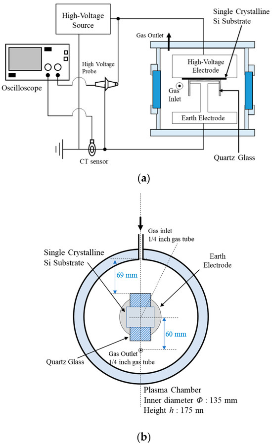
Figure 1.
Schematic diagrams depicting (a) an overview of the atmospheric pressure surface discharge plasma generation system and (b) a layout diagram viewed from above, illustrating the lower electrode with the positioned silicon substrate.
The gas flow rate was precisely controlled using mass flow controllers from Hitachi Metals, Ltd., Tokyo, Japan (model SFC-280E) and HORIBA STEC, Co., Ltd., Kyoto, Japan, (model SECE40MK310LMArSW), allowing adjustments from 0 to 6000 sccm. The gas entered the discharge vessel through a 1/4-inch outer diameter tube and exited from the upper section of the vessel. The alignment between the gas supply and exhaust ports is shown in Figure 1b. The gas inlet is located 69 mm from the edge of the concave quartz glass and 15 mm below the top surface of the concave dielectric, while the exhaust port is positioned approximately 60 mm from the central axis of the cylindrical discharge vessel, which has an inner diameter of 135 mm and a height of 175 mm.
The discharge-generating gas, a mixture of CF4 and Ar, is introduced at atmospheric pressure (P = 101 kPa) and expelled from the upper section of the vessel. A high-frequency power source (Logy Electric Co., Ltd., Tokyo, Japan, model HLV-10AC) operating at 9 kHz supplies voltage to the high-voltage-side electrode to initiate the surface discharge plasma. The discharge-sustaining voltage and current were measured using a high-voltage probe (Nissin Pulse Electronics, Chiba, Japan, EP-50K) and a CT sensor (Pearson, London, UK, Model 150), respectively. The etching profile of the monocrystalline Si substrate was assessed after post-treatment using a laser microscope (Olympus LEXT OLS400, Tokyo, Japan).
3. Experimental Results
This report details the etching process of a monocrystalline silicon substrate using surface discharge plasma generated at varying gas flow rates of Ar/CF4 mixed gas ranging from 0 to 6000 sccm. The resulting etching profile illustrates the impact of these variations on the material’s etching. Figure 2 displays a photograph of the surface discharge plasma, highlighting its generation near the triple junction point of the silicon substrate, discharge gas, and quartz glass (dielectric), and extending along the quartz surface. Notably, the plasma generated along the dielectric (quartz glass) consists of numerous filament-like surface streamers, indicating that etching occurs near the triple junction point where the plasma is generated, the extent of which depends on the shape of the dielectric and the diameter of the filamentary surface streamer.
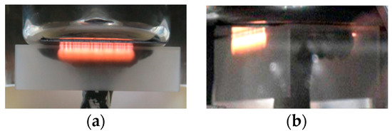
Figure 2.
Photo of surface discharge plasma generated under Ar/CF4 mixed gas: (a) Side view of the concave dielectric captured from the front. (b) Side view of the concave dielectric captured diagonally from the front.
Figure 3 depicts the waveforms of discharge current and voltage during the generation of surface discharge plasma with a flow rate of Ar and CF4 mixed gas at 6000 sccm and a discharge-sustaining voltage (Vpp) of 8.4 kV. The mixture of Ar and CF4 maintains a ratio of 7:3, corresponding to flow rates of 4200 sccm for Ar and 1800 sccm for CF4. The discharge voltage waveform is characterized as a pulse with a repetition frequency of 9.0 kHz. The discharge current consists of a displacement current, which arises due to a minor spatial gap between the metal electrode and the dielectric and the capacitance of the dielectric, as well as a pulse current generated by the initiation of surface streamers.
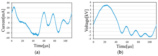
Figure 3.
(a) Discharge current waveform and (b) discharge voltage waveform due to surface discharge plasma generated at an Ar/CF4 gas flow rate of 6000 sccm and a discharge-sustaining voltage (Vpp) of 8.4 kV.
Figure 4 presents a three-dimensional representation of a groove formed by etching using surface discharge plasma. The specified flow rates of Ar and CF4 mixed gas are 0 sccm and 3000 sccm, respectively. A gas flow rate of 0 sccm indicates a condition in which the discharge-generated gas is confined within the discharge vessel, maintaining a gas mixture ratio of Ar to CF4 at 7:3. Conversely, at a flow rate of 3000 sccm, the respective flow rates for Ar and CF4 are 2100 sccm and 900 sccm. The discharge-sustaining voltage and the duration of the etching treatment are maintained at 9.4 kV and 5 min, respectively. Notably, etching by the surface discharge plasma progresses linearly along the concave quartz glass. The etching rate is at its maximum at the center of the filamentary surface streamer and gradually decreases with increasing distance from the streamer’s center, resulting in a gently sloping valley-shaped etching cross-section.
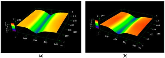
Figure 4.
Surface structure of silicon substrate obtained after etching by surface discharge plasma generated under Ar/CF4 mixed gas. (a) Ar/CF4 gas flow 0 sccm; (b) Ar/CF4 gas flow 3000 sccm.
Figure 5 clarifies the definition of groove width induced by surface discharge. Assessing the etching scenario along the width direction poses a challenge in determining the starting point of groove formation. Therefore, in this study, groove widths at depths of 0.2D and 0.8D relative to the total etching depth (D) are designated as W0.2 and W0.8, respectively. Subsequently, the etching progressions along the depth (D) and width (W0.2 and W0.8) directions via surface discharge plasma were evaluated.
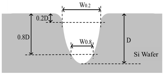
Figure 5.
Methodology for evaluating grooves formed on a silicon substrate through etching with surface discharge plasma.
In Figure 6, the relationship between the depth and width of grooves formed on the silicon substrate surface through surface discharge plasma etching at various argon (Ar) and carbon tetrafluoride (CF4) gas flow rates, dependent on the discharge-sustaining voltage, is depicted. The etching duration for the silicon substrate was held constant at 5 min. Due to the complexity of comparing etching depth and width at each flow rate using a three-dimensional image captured by laser microscopy, the average etching depth and width derived from these images were used for the analysis.
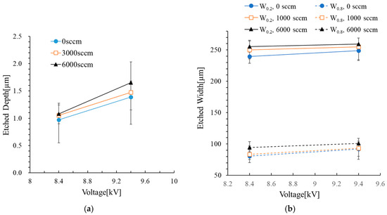
Figure 6.
Dependence of (a) etched depth and (b) etched width on the silicon substrate surface by surface discharge plasma at various Ar/CF4 gas flow rates relative to the discharge-sustaining voltage.
The analysis in Figure 6 reveals that grooves created by surface discharge plasma expand in both depth and width as the flow rate of the Ar and CF4 mixed gas increases. This expansion is attributed to the increased presence of Ar ions and active species in the plasma, which is facilitated by an elevation in the discharge-sustaining voltage. Furthermore, a higher discharge-sustaining voltage leads to more pronounced etching in both the depth and width directions. This increase is due to the higher abundance of active species that promote etching and diffuse more broadly in the width direction as the discharge-sustaining voltage increases.
Figure 7 illustrates the changes in groove depth and width through surface discharge plasma etching at different Ar and CF4 gas flow rates, as a function of etching time. The data indicate that silicon etching advances in both depth and width with increasing flow rates of the Ar/CF4 mixed gas. Moreover, prolonging the etching treatment duration leads to further development of silicon etching in both depth and width directions. The surface discharge plasma exhibits a columnar shape with a diameter of approximately 200 μm, and the dielectric is formed by a rectangular dielectric electrode. Hence, etching in the width direction occurs through the diffusion of active radical species, such as Fx and CFn, resulting in a gradual deceleration of etching progression in the width direction beyond the surface discharge plasma region.
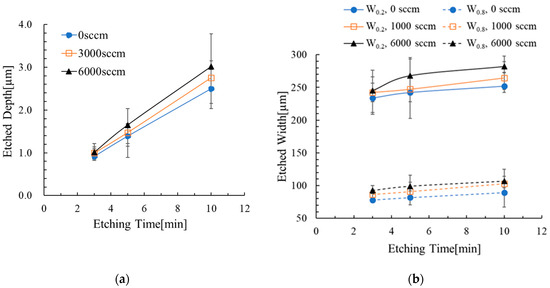
Figure 7.
Dependency of (a) etched depth and (b) etched width on the silicon substrate surface during etching using surface discharge plasma generated at various Ar/CF4 gas flow rates.
4. Discussion
In this study, surface discharge plasma under atmospheric pressure conditions was utilized with Ar and CF4 mixed gas to etch monocrystalline silicon substrates. The study focused on examining the etching characteristics of silicon substrates as a function of changes in the flow rate of Ar/CF4 mixed gas. The findings indicate that within a flow rate range of 0 to 6000 sccm, higher flow rates of the Ar/CF4 mixed gas are associated with increased etching of silicon in both depth and width. The etching mechanism primarily involves the bombardment of the substrate by Ar ions produced in the plasma, along with a chemical reaction involving active species such as Fx and CFn. These species are generated as CF4 dissociates, a process facilitated by collisions between electrons, which are accelerated by an electric field, and metastable excited Ar species (11.6 eV, 11.8 eV) interacting with CF4 molecules. The specific dissociation reactions of CF4 and the energies required for these reactions are outlined in Equations (1)–(8).
CF4 → CF3 + F 5.60 [eV]
CF4 → CF2 + F2 7.81 [eV]
CF4 → CF2 + 2F 9.46 [eV]
CF3 → CF2 + F 3.80 [eV]
CF2 → CF + F 5.40 [eV]
CF2 → C + 2F 11.00 [eV]
CF → C + F 5.60 [eV]
F2 → 2F 4.34 [eV]
Active species such as F, F2, and CFn, generated through the reactions specified in Equations (1)–(8), are thought to play a crucial role in facilitating the etching process. Figure 8 displays the emission spectrum of the atmospheric pressure surface discharge plasma, measured using a multichannel spectrometer (USB4000, Ocean Optics Inc., Orlando, FL, USA, wavelength resolution 1.5 nm). Within this figure, peaks attributed to F, Ar, and CFn were identified in the plasma produced by the Ar/CF4 mixed gas [17]. Line spectra originating from Ar and F typically appeared at wavelengths of 763.5105 nm and 634.851 nm, respectively [18]. In the current measurement, a line spectrum due to Ar was detected at a wavelength of 763.78 nm, along with a band spectrum attributed to F centered at approximately 630 nm. Accordingly, this study focused on a wavelength of 631.45 nm, corresponding to the peak emission intensity within the F-band spectrum. Figure 9 illustrates the emission spectrum intensities of the excited species stimulated by Ar (763.78 nm), F (631.45 nm), and CFn (327.54 nm) at various gas flow rates. As the presence of CFn was confirmed through its band spectrum, the study particularly noted the emission intensity at 327.54 nm, representing the peak of this band spectrum. As the gas flow rate increased, the emission intensities of F and CFn, the key species in the etching process, also increased. Conversely, the variation in the emission intensity of the Ar peak with increasing gas flow rate remained negligible. Given the inert nature and low reactivity of Ar, minimal changes due to variations in the gas flow rate are expected. Therefore, an increase in the gas flow rate is presumed to enhance the generation of active species, such as Fx and CFn, thereby promoting the progression of silicon etching.
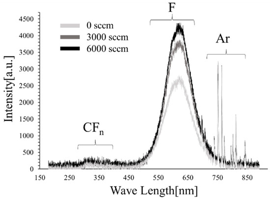
Figure 8.
Emission spectrum of surface discharge plasma generated at different Ar/CF4 gas flow rates (measured wavelength: 180–900 nm, discharge-sustaining voltage: 9.4 kV).
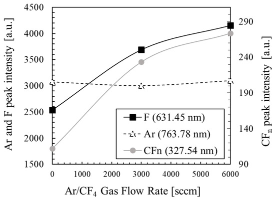
Figure 9.
Changes in Ar, F, and CFn emission intensities in surface discharge plasma at various Ar/CF4 gas flow rates (F peak: 631.45 nm, Ar peak: 763.78 nm, CFn peak: 327.54 nm).
Figure 10 illustrates the discharge power at various Ar/CF4 mixed gas flow rates. The discharge power was calculated as the average power derived from one cycle of the discharge voltage and current waveform during the silicon substrate etching process. Throughout the measurements, the discharge-sustaining voltage was maintained at 9.4 kV. As depicted in Figure 10, the discharge power remained approximately 10 W across all gas flow rates. However, a noticeable trend of increasing discharge power with higher flow rates of Ar/CF4 gas was observed. This increase in discharge power, corresponding with higher Ar/CF4 gas flow rates, suggests a concurrent rise in the quantity of active species such as Ar ions and CFn, which play a critical role in the etching process.
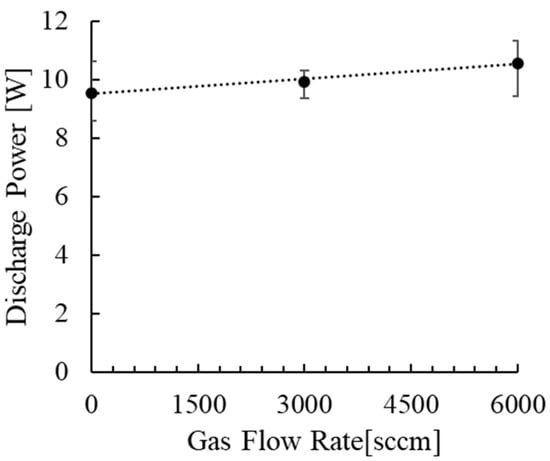
Figure 10.
Relationship between Ar/CF4 mixed gas flow rate and discharge power.
Etching via surface discharge relies on a filament-like surface streamer, roughly 200 µm wide [10]. Beyond the reach of this streamer in the width direction, etching occurs through the diffusion of active species like F, F2, and CFn, generated within the surface discharge plasma. As the Ar/CF4 gas flow rate increases, not only does the generation of these active species conducive to etching rise, but they also diffuse more extensively due to the heightened gas flow rate, thereby bolstering etching in the width direction. Additionally, the effectiveness of removing etching byproducts from the plasma region to exterior regions via high gas flow before they can redeposit improves with increased gas flow rate, thus expediting the silicon etching process.
Under these experimental conditions, elevating the gas flow rate enhanced the etching efficiency of Si. However, surpassing a certain threshold in increasing the flow rate of the Ar and CF4 mixed gas to the plasma region could induce plasma instability, potentially diminishing both the etching rate and uniformity. Hence, optimizing the gas flow rate is pivotal in surface discharge plasma etching to guarantee consistent and efficacious outcomes.
5. Conclusions
Our investigation delved into the impact of gas flow rate on silicon etching using surface discharge plasma. Our findings unequivocally showcased a direct correlation between escalated Ar and CF4 mixed gas flow rates and heightened etching rates of Si, spanning both width and depth. Emission spectroscopy analysis unveiled a surge in plasma emission intensities attributed to the F and CFn species, signaling an augmentation in the generation of active species pivotal for the etching process. Furthermore, amplifying the Ar/CF4 gas flow rate not only bolstered the production of these active species but also facilitated their diffusion across a broader expanse. This enhancement significantly contributed to the progression of etching in the width direction. Additionally, a higher gas flow rate deterred the deposition of etching byproducts within the plasma region, thereby smoothing the path for silicon etching. Future avenues encompass the refinement of power supplies to enable swifter and finer processing and the optimization of surface discharge plasma generation conditions.
Author Contributions
Conceptualization, T.H.; methodology, T.H. and K.N.; validation, T.H. and K.N.; investigation, T.H. and M.Y.; data curation, T.H., K.N. and M.Y.; writing—original draft preparation, T.H.; writing—review and editing, T.H., K.N. and M.Y.; visualization, T.H. and K.N.; supervision, T.H.; project administration, T.H. All authors have read and agreed to the published version of the manuscript.
Funding
This research received no external funding.
Institutional Review Board Statement
Not applicable.
Informed Consent Statement
Not applicable.
Data Availability Statement
Data will be made available on request.
Conflicts of Interest
The authors declare no conflicts of interest.
References
- Stefecka, M.; Korzec, D.; Siry, M.; Imahori, Y.; Kando, M. Experimental Study of Atmospheric Pressure Surface Discharge in Helium. Sci. Technol. Adv. Mater. 2001, 2, 587–593. [Google Scholar] [CrossRef]
- Cejas, E.; Mancinelli, B.; Prevosto, L. Modelling of an Atmospheric–Pressure Air Glow Discharge Operating in High–Gas Temperature Regimes: The Role of the Associative Ionization Reactions Involving Excited Atoms. Plasma 2020, 3, 12–26. [Google Scholar] [CrossRef]
- Li, S.; Sun, J.; Sun, R.; Pan, J.; Wang, L.; Chen, C.; Chen, Q.; Liu, Z. Spatiotemporal characteristics of radio frequency dielectric barrier glow discharge at atmospheric pressure. Appl. Sci. 2021, 11, 8430. [Google Scholar] [CrossRef]
- Jang, H.J.; Jung, E.Y.; Parsons, T.; Tae, H.-S.; Park, C.-S. A review of plasma synthesis methods for polymer films and nanoparticles under atmospheric pressure conditions. Polymers 2021, 13, 2267. [Google Scholar] [CrossRef] [PubMed]
- Stryczewska, H.D.; Boiko, O. Applications of plasma produced with electrical discharges in gases for agriculture and biomedicine. Appl. Sci. 2022, 12, 4405. [Google Scholar] [CrossRef]
- Li, S.; Sun, J.; Sun, R.; Pan, J.; Wang, L.; Chen, C.; Chen, Q.; Liu, Z. Characteristics of Radio Frequency Dielectric Barrier Discharge Using Argon Doped with Nitrogen at Atmospheric Pressure. Materials 2022, 15, 7647. [Google Scholar] [CrossRef] [PubMed]
- Huff, M. Recent advances in reactive ion etching and applications of high-aspect-ratio microfabrication. Micromachines 2021, 12, 991. [Google Scholar] [CrossRef] [PubMed]
- Chircov, C.; Grumezescu, A.M. Microelectromechanical systems (MEMS) for biomedical applications. Micromachines 2022, 13, 164. [Google Scholar] [CrossRef] [PubMed]
- Hamada, T.; Masuda, S.; Nishida, K.; Yamamoto, S. Etching Characteristics of SixNy Film on Textured Single Crystalline Silicon Surface using Ar/CF4 and He/CF4 Surface Discharge Plasma. Coatings 2020, 10, 563. [Google Scholar] [CrossRef]
- Hamada, T.; Sakoda, T.; Otsubo, M. Studies on non-thermal atmospheric pressure plasma process conditions for groove formation on silicon nitride for silicon solar cells. Mater. Sci. Semicond. Process. 2009, 12, 106–112. [Google Scholar] [CrossRef]
- Bagher, A.M.; Vahid, M.M.A.; Mohsen, M. Types of Solar Cells and Application. Am. J. Opt. Photonics 2015, 3, 94–113. [Google Scholar] [CrossRef]
- Liu, J.; Yao, Y.; Xiao, S.; Gu, X. Review of status developments of high-efficiency crystalline silicon solar cells. J. Phys. D 2018, 51, 123001. [Google Scholar] [CrossRef]
- Wang, S.; Mai, L.; Wenham, A.; Hameiri, Z.; Payne, D.; Chan, C.; Hallam, B.; Sugianto, A.; Chong, C.M.; Ji, J.; et al. Selective emitter solar cell through simultaneous laser doping and grooving of silicon followed by self-aligned metal plating. Sol. Energy Mater. Sol. Cells 2017, 169, 151–158. [Google Scholar] [CrossRef]
- Sui, M.; Chu, Y.; Zhang, R. A review of technologies for high efficiency silicon solar cells. J. Phys. Conf. Ser. 2021, 1907, 1–15. [Google Scholar] [CrossRef]
- Nagel, H.; Aberle, A.G.; Hezel, R. Optimised antireflection coatings for planar silicon solar cells using remote PECVD silicon nitride and porous silicon dioxide. Prog. Photovolt. 1999, 7, 245–260. [Google Scholar] [CrossRef]
- Abdullah, M.; Alghoul, M.; Naser, H.; Asim, N.; Ahmadi, S.; Yatim, B.; Sopian, K. Research and development efforts on texturization to reduce the optical losses at front surface of silicon solar cell. Renew. Sustain. Energy Rev. 2016, 66, 380–398. [Google Scholar] [CrossRef]
- Wang, R. Microsecond pulse driven Ar/CF4 plasma jet for polymethylmethacrylate surface modification at atmospheric pressure. Appl. Surf. Sci. 2015, 328, 509–515. [Google Scholar] [CrossRef]
- Lee, J. On the relationship between plasma chemistry, etching kinetics and etching residues in CF4+C4F8+Ar and CF4+CH2F2+Ar plasmas with various CF4/C4F8 and CF4/CH2F2 mixing ratios. Vacuum 2018, 148, 214–223. [Google Scholar] [CrossRef]
Disclaimer/Publisher’s Note: The statements, opinions and data contained in all publications are solely those of the individual author(s) and contributor(s) and not of MDPI and/or the editor(s). MDPI and/or the editor(s) disclaim responsibility for any injury to people or property resulting from any ideas, methods, instructions or products referred to in the content. |
© 2024 by the authors. Licensee MDPI, Basel, Switzerland. This article is an open access article distributed under the terms and conditions of the Creative Commons Attribution (CC BY) license (https://creativecommons.org/licenses/by/4.0/).