Abstract
Improvement in crystallinity was investigated by compensating for stoichiometric deviations of non-selenization processed Cu0.9In0.7Ga0.3Se2 (CIGS) thin films due to highly volatile Se by co-sputtering them with Te followed by rapid thermal annealing. The prepared CIGS:Te thin films did not show any linear correlation between the compositional ratio and the co-sputtering time of Te; however, the deviation parameter (Δs) from the stoichiometry and normalized stoichiometric deviations of Se + Te and In + Ga were largely consistent with the behavior of thin-film properties. The proposed method provides better crystallinity with a large grain size, clear grain boundaries, and low microstrain and dislocation density, resulting in a large volume of the unit cell. The CIGS:Te thin films used as absorbers show improved optical properties compared to the conventional CIGS thin films, with Eg = 1.548 eV. These results can advance the low-cost commercialization of the enhanced-efficiency CIGS:Te thin films without the selenization process.
1. Introduction
Chalcopyrite Cu–III–VI2 (III = In, Ga, Al; VI = Te, S, Se) semiconductors such as CuAlSe2 (CAS), CuInSe2 (CIS), CuIn1−xAlxSe2 (CIAS), CuIn1−xGaxSe2 (CIGS), and CuIn1−xGax(Se1−ySy)2 (CIGSS) are promising materials for thin film solar cells [1,2,3]. Among them, CIGS has been extensively studied because of its high optical absorption (>105 cm−1), tunable band gap (Eg) from 1.011 eV (CIS) to 1.676 eV (CGS), excellent electro–optical stability, low-cost raw materials, non-use of toxic or hazardous polluting substances, and long-term electrothermal stability [4,5]. A co-evaporation and post-selenization process for CIGS thin films is well established [6]; however, it has several disadvantages, including the complexity of the process with expensive equipment, slow reaction rate, and poor adhesion to the back contact [7,8,9]. Several efforts have been made to develop an eco-friendly and inexpensive method for the one-step fabrication of CIGS thin films without an additional selenization or sulfurization process [10,11,12]; nevertheless, the loss of Se in the thin films due to volatilization during heat treatment could not be suppressed [13,14,15,16,17]. In previous studies, this non-selenization method was performed to prepare CI(G)S thin films with Se-rich precursors, considering the vaporization of Se in advance by adjusting the temperature and time using a rapid thermal annealing (RTA) process in ambient N2 gas [12,13]. Although the crystallinity and optical properties of the CI(G)S thin films could be improved by slightly supplementing the Se composition, a stoichiometric CI(G)S thin film could not be prepared [13]. Substitutional doping by partial replacement of Se with Te can contribute to an increase in the band gap of the CuInGa(Se,Te)2 (CIGST) absorber, allowing it to participate in p–d and s–p transitions for increasing the uncertainties in band structure with a lower barrier height for p–n junction formation [18,19]. Although this gives a corresponding loss of photocurrent, this can enhance the open-circuit voltage (Voc) by increasing the band gap of the absorber layer by compensating for Se vacancies [18,20]. Magnetron sputtering has the advantages of excellent composition transfer, superior adhesion of thin films, straightforward control of the deposition rate, uniform surface morphology, possibility of large-area deposition, and low-cost and full-vacuum equipment [21,22]. Moreover, the co-sputtering process can be performed as a one-step process with control over the composition of the films without the use of toxic or explosive chemicals or high-cost equipment for the selenization process. The focus of this study is to examine the effect of Te incorporated into the space charge region of CIGS thin films prepared using radio frequency (RF) magnetron co-sputtering equipment with Cu0.9In0.7Ga0.3Se2 and Te targets. A series of Te-doped CIGS (CIGS:Te) thin films were fabricated with different Te contents at a constant total thickness, which was controlled by the deposition time for the Te target. Then, all the precursors were annealed by using a rapid thermal annealing (RTA) system to prevent the volatilization of Se and Te-nonhomogeneity.
2. Materials and Methods
CIGS:Te thin films were deposited on 2 cm × 2 cm Corning glass using an RF magnetron co-sputtering equipment (IDT Engineering Co., Gyeonggi, Republic of Korea) [21], with 5.08-cm-diameter CIGS (RNDKorea Corp., Gyeonggi, Republic of Korea, Cu0.9In0.7Ga0.3Se2, 99.99%-purity) and Te (RNDKorea Corp., 99.99%-purity) targets at fixed powers of 35 W and 10 W, respectively. All samples were fabricated under the following fixed conditions: pre-sputtering for 3 min at each run, base pressure of 133.3224 × 10⁻⁶ Pa, Ar gas flow rate of 50 sccm, frequency of 13.56 MHz, and working pressure of 999.9178 × 10⁻³ Pa with a substrate-to-target distance of 5.0 cm during sputtering at room temperature. The deposition time for the Te target was varied from 0 to 1140 s to obtain a Te thickness of 0 to 88 nm at a constant thickness of approximately 400 nm, while the total deposition time was adjusted from 3600 to 2916 s for the proper comparison of optical properties. The deposition rates of CIGS and Te were 6.67 and 4.00 nm/min at the process condition, respectively. The estimated or expected thicknesses of Te were (1) 0, (2) 18, (3) 34, (4) 50, (5) 63, and (6) 76 nm, deposited at various co-sputtering times for Te target of (1) 0, (2) 270, (3) 510, (4) 750, (5) 945, and (6) 1140 s, respectively, keeping the total thickness of the CIGS:Te thin films at 400 nm (Figure S1). The measured total thickness of the CIGS:Te thin films was 397–417 nm (Figure S2), which is not significantly different from the target thickness. After the co-sputtering deposition of the non-equilibrium CIGS:Te thin films, the samples were subjected to RTA (GRT-100, GD-Tech Co., Gyeongsangbuk, Republic of Korea) at 400 °C for 20 min under a N2 gas atmosphere (Figure S1).
The crystalline structures of the films were analyzed using X-ray diffraction (XRD, PANalytical B.V., Almelo, The Netherlands, X’pert-PRO-MRD, Cu Kα = 0.15405 nm, 40 kV, 30 mA) over a 2θ range of 10°–90° with a step size of 0.026° and scanning speed of 8.5°/min. Field emission scanning electron microscopy (FESEM, JEOL, Tokyo, Japan, JSM-7500F) was used to reveal the morphological characteristics of the CIGST thin films. An energy dispersive X-ray spectroscope (EDX, Oxford Instruments, Abingdon, Oxfordshire, UK, INCA) attached to the FESEM was used to characterize the chemical composition of the CIGS:Te thin films. The optical and electrical properties of the CIGST thin films were measured using an ultraviolet–visible (UV) spectrophotometer (Varian Techtron, Mulgrave, Australia, Cary500 scan) over a range of 200–2000 nm and a Hall-effect measurement system (Accent Optical Technologies, Bend, OR, USA, HL5500PC) at room temperature, respectively.
3. Results and Discussion
FESEM was used to analyze the surface morphologies of the RTA-treated CIGS:Te thin films with different co-sputtering times for the Te target. The top-view FESEM images of the CIGS/CIGS:Te thin films shown in Figure 1 show no extended cracks after the RTA treatment [23,24]. The fine grains were tightly connected, with a relatively indistinct boundary in the CIGS thin film, as shown in Figure 1a. No significant difference between the CIGS:Te thin film with a Te co-sputtering time of 270 s (Figure 1b) and the CIGS thin film (Figure 1a) was observed, except for slightly larger grains in the former. For the CIGS:Te thin film with a Te co-sputtering time of 510 s (Figure 1c), the grains accumulated to form larger grains with clear boundaries after RTA treatment despite the same conditions. Large features were observed on the surfaces of the CIGS:Te thin film, as shown in Figure 1c, similar to the larger grains on the smaller grain background in CIGST and Cu(In,Ga)Te2 (CIGT) thin films formed by compositional variations [1,25]. Well-defined and dense grains with distinct boundaries were also observed in the CIGS:Te thin films with Te co-sputtering times of 750 s (Figure 1d) and 945 s (Figure 1d). At a Te co-sputtering time of 1140 s (Figure 1f), the grains became very small with a blurred boundary as the thickness ratio of Te during the co-sputtering of CIGST:Te thin films increased, and the surface characteristics changed with no consistent tendency.
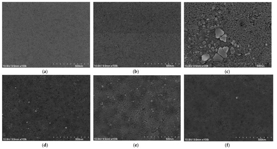
Figure 1.
Top-view field emission scanning electron microscopy (FESEM) surface images of the CIGS:Te thin films with Te co-sputtering times of: (a) 0, (b) 270, (c) 510, (d) 750, (e) 945, and (f) 1140 s.
The compositional characteristics of RTA-treated CIGS:Te thin films fabricated at different Te co-sputtering times were examined using EDX. Considering the different deposition rates of the Te/CIGS targets, thickness ratios for all 400-nm-thick CIGS:Te thin films were estimated. The expected thickness ratios of Te/CIGS were 0/400, 18/382, 34/366, 50/350, 63/337, 76/324, and 88/312 nm at the co-sputtering times for each target shown in Figure 2a, which correspond to the compositional ratios, Te/(Se + Te), of 0.0, 10.3, 15.7, 22.2, 27.2, 31.9, and 36.1%, respectively. However, the atomic percentage of Te/(Se + Te) after the Te co-sputtering was in the range of 4.2–6.0%. The increase was not linear but showed slight ups and downs. Controlling the compositional ratio by controlling the thicknesses of the elemental layers within the precursor stack is reported to be difficult, even with RTA treatment after the evaporation of the stacks [1]; additionally, controlling the compositional ratio by adjusting the deposition rates in the co-sputtering method is also not easy. All the CIGS:Te thin films prepared using the Cu0.9In0.7Ga0.3Se2 target showed Cu-poor compositions, and the CIGS thin film without Te exhibited a Cu-poor composition of around 22.4%, as shown in condition (1) of Figure 2b, which also clearly shows the lack of Se with a composition of around 45.8%. The atomic percentage of In + Ga remained relatively even, within the range of 28.5–32.0% under all conditions. Once Te was co-sputtered, the relative atomic percentage of Se + Te increased by approximately 4%. After increasing the Te co-sputtering time, the relative atomic percentage of Te in the CIGS:Te thin films tended to be similar or slightly reduced, while the relative atomic percentage of Se was constant overall but partially large, even though they were samples that used the same target. The relative atomic percentage of Cu in the CIGS:Te thin films increased and then decreased under the condition (6) after becoming constant, and the relative atomic percentage of Se tended to be inversely proportional to Cu under these conditions. When examining the relationship between the surface morphologies and the change in the relative atomic percentage of the individual elements in the CIGS:Te thin films, an increase in the relative atomic percentage of Cu and a decrease in the relative atomic percentage of Se were noticeable under the condition (6) where the very small grains with indistinct boundaries appeared. According to previous studies [1,26], changes in the surface properties of CIGS/CIGST thin films have been observed with a variation in the compositional ratios of Ga/(Ga + In) and Te/(Se + Te); however, the changes in the surface properties of Te/(Se + Te) were not significant, as shown in Figure 2a. To examine the contribution of certain compositional ratios in the CIGS:Te thin films to the surface properties more closely, various compositional ratios other than Ga/(Ga + In) are shown in Figure 2c. Because the change in the relative atomic percentage of Te over Te-sputtering time was very small, the change in the relative atomic percentages of Se + Te was determined by that of Se, and the surface morphology showed the most similar tendency to the change in the compositional ratio of (Se + Te)/(Cu + In + Ga). This is a different result from that for Ga/(Ga + In), known as a prevailing influence factor on the surface morphology in Cu-rich thin films [1,26], and seems not to be applied under Cu-poor conditions with better energy conversion efficiency. A more rigorous relationship must be investigated. Two parameters, Δm and Δs, were examined to determine deviations from molecularity and stoichiometry, respectively: Δm = [Cu]/([In] + [Ga]) − 1 and Δs = 2([Se] + [Te])/([Cu] + 3[In] + 3[Ga]) − 1 [2,27,28,29]. The parameters Δm and Δs refer to deviations from the molecularity and valance stoichiometry, respectively. For stoichiometric compounds, the parameters exhibited no deviations. Figure 2d shows Δm and Δs in the non-stoichiometric CIGS:Te thin films at different co-sputtering times for the Te target. The chemical compositions of the CIGS:Te thin films were analyzed by extracting their atomic percentage using EDX. Δm < 0 and Δs < 0 ((Se + Te)-poor) compositions were obtained for all the CIGS:Te thin films, regardless of the Te co-sputtering time. While CIGS thin film without Te had Δm = −0.296 and Δs = −0.224, the non-stoichiometric CIGS:Te thin films showed Δm = (2) −0.258, (3) −0.245, (4) −0.231, (5) −0.231, and (6) −0.134 as the Te co-sputtering time was increased. The Δs values were (2) −0.080, (3) −0.067, (4) −0.128, (5) −0.116, and (6) −0.226, respectively. The value in the non-stoichiometric CIGS:Te thin films under the condition (3) was closest to ‘0’, and it was the furthest away under condition (6). Note that Δs in the Δm < 0 CIGS:Te thin films used in this study showed a similar tendency as those of the surface properties. Under the condition that the compositional ratio of chalcogens increased and those of metals decrease at the same time, surface properties, such as grain size and clarity of grain boundaries, were also improved; that is, the Δs approached the stoichiometric composition. In the opposite case, the surface properties degraded. In this study, a normalized deviation from the stoichiometric composition for each element group is proposed and applied to the pentary compound CIGS:Te. The normalized stoichiometric deviation is calculated for each element group by taking the absolute values and is defined as follows: N[In+Ga] = 1 − |[(In + Ga)exp] − [(In + Ga)ideal]|/[(In + Ga)ideal], which converges to ‘1’ when each element group is close to the stoichiometric composition. The deviations from the stoichiometric compositions of Cu, In + Ga, and Se + Te in the CIGS thin films without Te sputtering were −2.59, 6.83, and −4.24, respectively. In the case of Cu, negative values were observed under all conditions except (6), and the deviation was in the range of −3.58–0.79. The deviations for In + Ga and Se + Te were in the ranges of +3.52 to +4.74 and −0.06 to −5.49, respectively, under all conditions where Te was sputtered, as shown in Figure 2b. The effects were more clearly investigated when each deviation was normalized for the ideal stoichiometry, as plotted in Figure 2e. The CIGS thin film prepared via RTA after sputtering had many Se vacancies in a Se-poor state, as shown in Figure 2e; however, the normalized stoichiometric deviation for Se + Te was close to ideal stoichiometry under condition (3) once stoichiometric compensation was performed by Te co-sputtering, while it was the largest under condition (6). Although it could not be confirmed in Figure 2b,d, the normalized stoichiometric deviation for In + Ga also changed dramatically, as shown in Figure 2e. Under all conditions, In + Ga was in a surplus state and showed the largest deviation in the CIGS thin film (condition (1)), but after the Te co-sputtering, even the In + Ga changed more closely to stoichiometry in all the CIGS:Te thin films. In particular, In + Ga was in the smallest excess state under condition (3) and changed to the most non-stoichiometric deviation under condition (6) of the CIGS:Te thin films. The normalized stoichiometric deviation of each element group showed a similar tendency to change, with CIGS thin films being the most non-stoichiometric, while the most stoichiometric and non-stoichiometric compositions were obtained under conditions (3) and (6) of the CIGS:Te thin films, respectively.
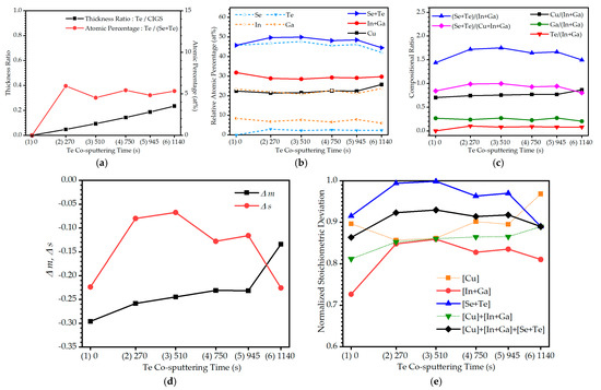
Figure 2.
Energy dispersive X-ray spectroscope (EDX) analyses of the CIGS:Te thin films with different Te co-sputtering times of (1) 0, (2) 270, (3) 510, (4) 750, (5) 945, and (6) 1140 s. (a) Thickness ratio and atomic percent, (b) relative atomic percentage, (c) compositional ratio, (d) deviation parameters from the molecularity and the stoichiometry, Δm and Δs, and (e) normalized stoichiometric deviations.
Figure 3a shows the XRD patterns of the RTA-treated CIGS:Te thin films at different co-sputtering times for the Te target in the 2θ range of 10°–90°. The XRD patterns exhibited an enhanced crystalline quality in the CIGS:Te thin films without selenization after 20 min of RTA treatment at 400 °C, which did not contain any appreciable amounts of elemental phases or secondary phases such as Te and InTe after the RTA treatment [25]. This is believed to be because Te atoms replace Se vacancies, and all samples show (Se + Te)-poor conditions, leaving no extra Se or Te atoms to appear in the form of elemental phases or secondary phases. The CIGS:Te thin films showed major diffraction peaks corresponding to the CIGS chalcopyrite phases with preferred orientations of (112), (220/204), and (312) at 2θ = 26.71°, 44.28°, and 52.47°, respectively. The major diffraction peaks became sharper and stronger under condition (3). Closest to the stoichiometric composition under condition (3), the normalized stoichiometric deviation for Se + Te was observed to have a greater impact on the crystallinity. The major diffraction peaks were also observed to become less sharp under condition (6), which has the highest (Se + Te)-vacancy and the highest In + Ga surplus. As shown in Figure 2b,c, the change in the relative atomic percentage and compositional ratio was not significant under condition (6). The diffraction peaks of the CIGS:Te thin films under these conditions indicated that grain growth and crystallinity of the thin films occurred along the (112)-, (220/204)-, and (312)-oriented crystallographic CIGS planes. This confirms that Te co-sputtering can achieve good crystallographic quality and grain growth because Te fills the Se vacancies to reduce crystal defects. Acceptable electrical properties, including Voc and the short-circuit current density (Jsc), can be obtained by reducing both carrier recombination and the leakage current originating from the structural defects in the thin films by using densely packed (112)-, (220/224)-, and (312)-oriented grains [10,27]. The full width at half maximum (FWHM) of the (112) diffraction peaks, as a function of Te co-sputtering time, is shown in Figure 3b. The FWHM of the CIGS thin film decreased from 1.1082° to 0.5635° under condition (3) of the CIGS:Te thin film after Te co-sputtering because of the closest stoichiometric condition, indicating fewer defects overall, including both Se vacancy and In + Ga interstitial. The crystallite sizes of the CIGS/CIGS:Te thin films were calculated from the (112) diffraction peak using the Debye–Scherrer formula, D = 0.94λ/ω·cosθ, where λ is the Kα radiation wavelength of Cu (λ = 0.15406 nm); ω is the FWHM of the (112) diffraction peak in radians; and θ is the Bragg angle corresponding to the (112) diffraction peak. The crystallite size of CIGS thin film without Te was 7.12 nm, which increased to 15.88 nm under condition (3), as shown in Figure 3b, whereas it reached a minimum value of 6.79 nm under condition (6). The average grain size is shown in Figure 3c, which was estimated using the FESEM images in Figure 1 and the ImageJ software [30]. Both, the crystallite size from XRD and average grain size from FESEM, showed a similar tendency with respect to Δs from EDX.
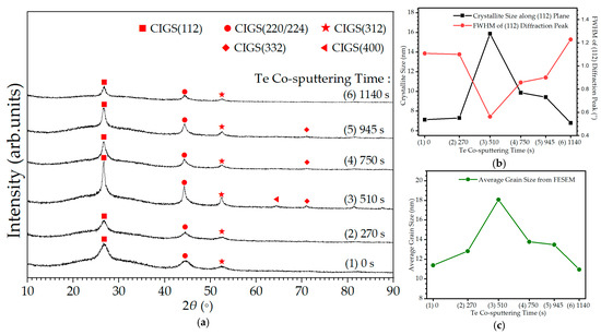
Figure 3.
(a) X-ray diffraction (XRD) patterns, (b) crystallite size along the (112) plane and full widths at half maximum (FWHM), and (c) average grain sizes of the CIGS:Te thin films with different Te co-sputtering times of (1) 0, (2) 270, (3) 510, (4) 750, (5) 945, and (6) 1140 s.
Figure 4a shows the interplanar distances corresponding to the d-spacings for tetragonal CIGS:Te orientation along the (112) plane, d112, at different co-sputtering times for the Te target. d112 was calculated using the equation d112 = λ/2sinθ, where λ is the Kα radiation wavelength of Cu (λ = 0.15406 nm) and θ is the Bragg angle corresponding to the diffraction peak obtained from the XRD data [31]. The d112 value of the CIGS:Te thin films was in the range of 0.333–0.334 nm, which agrees with a previous study [32]. The tetragonal distortion parameter η = c/a was in the range of 2.005–2.026. The diffraction data analysis with lattice constants a and c in a tetragonal chalcopyrite structure was performed using the equation 1/d2 = (h2 + k2)/a2 + l2/c2, combined with Bragg’s law, d = λ/2sinθ, where d is the spacing between the planes in the atomic lattice (interplanar spacing); hkl are Miller indices; λ is the wavelength of CuKα radiation; and θ is the angle between the incident ray and the scattering planes [33]. For a particular incident X-ray wavelength λ and angle θ from XRD, the d spacing can be determined from Bragg’s law. Lattice constants a and c can also be calculated using the (112), (220/204), and (312) peaks shown in Figure 4b. The lattice constants of the tetragonal CIGS:Te thin films are generally a = 0.56–0.58 nm and c = 1.10–1.15 nm [34]. For the CIGS thin films without Te, a and c were 0.575 and 1.164 nm, respectively. Lattice constant a gradually increased and then decreased, attaining a maximum value of 0.578 nm under condition (3) as the Te co-sputtering time increased. Lattice constant c instantly decreased as Te co-sputtering was performed, and it gradually decreased as a function of Te co-sputtering time in the CIGS:Te thin films, reaching a minimum value of 1.156 nm under condition (6). The volume of the unit cell was estimated from the expression for the tetragonal system: V = abc. When the volume of the unit cell in the CIGS thin film without Te was 384.12 × 10⁻³ nm3, the volumes of the unit cell of all CIGS:Te thin films were in the range of 384.56–387.92 × 10⁻³ nm3, which is higher than that of the CIGS thin films, as shown in Figure 4b. The diffraction peak corresponding to the (112) orientation also shifted to higher 2θ values, from 26.58°, for the CIGS thin film, to 26.71°, for the CIGS:Te thin films, when Te was co-sputtered, and then shifted to a lower 2θ value of 26.63° under condition (6). According to Bragg’s law, the shift in the Bragg angle was caused by a change in the spacing of the crystallographic planes, whereas strain increased the d-spacing, causing a shift in the Bragg angle of the diffraction peak towards lower 2θ values in the XRD pattern [35]. Figure 4c shows the microstrain (ε) due to distortions and crystal imperfections of the CIGS:Te thin films as calculated using the equation ε = ω·cosθ/4, where ω is the FWHM of the preferred diffraction peak in radians and θ is the Bragg angle corresponding to the predominant diffraction peak obtained from the XRD data [36,37,38,39]. The microstrain along the (112) orientation decreases from a minimum of 2.391 × 10⁻³ under condition (3) to a maximum of 5.210 × 10⁻³ under condition (6). The dislocation density (δ) was calculated using the equation Δ = 1/D2, where D is the mean crystallite size of the CIGS:Te thin films. The dislocation density exhibited a similar trend in the microstrain along the (112) orientation. The lowest value of 4.3629 × 10¹⁵ line/m2 was obtained under condition (3), when the dislocation density decreased from the highest value of 20.7105 × 10¹⁵ line/m2 under condition (6). This indicates that the largest crystallite size was obtained under condition (3) because of the released microstrain and dislocation density, as shown in Figure 1c. With an increase in the Te sputtering time for the strained CIGS thin film, the increased Te2+ ions occupied the Se vacancies, expanding the volume of the unit cell up to condition (3) as the strain was relieved rapidly by the compensated strain due to relaxation in the horizontal direction, whereas volumetric contraction occurred as the additional Te sputtering time increased up to the condition (f). As shown in Figure 2e, the normalized stoichiometric deviation of Se + Te decreased up to condition (6), that is, the number of Se + Te vacancies increased, causing the dislocation to increase again and resulting in a decrease in the volume of the unit cell, as shown in Figure 4c.
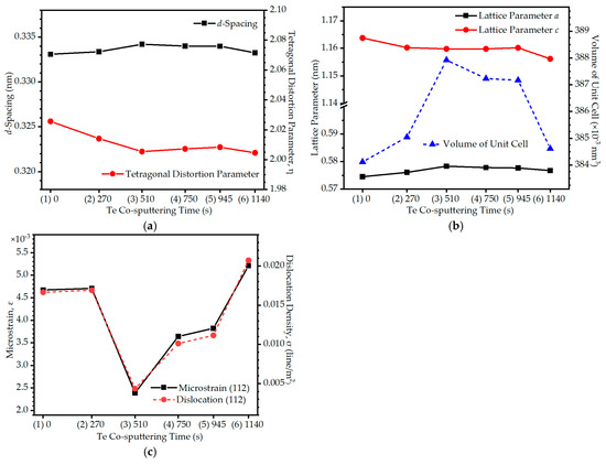
Figure 4.
Lattice characteristics of the CIGS:Te thin films with different Te co-sputtering times of (1) 0, (2) 270, (3) 510, (4) 750, (5) 945, and (6) 1140 s. (a) Tetragonal distortion parameter (η) and d-spacing along the (112) plane; (b) lattice constants, a and c, and volume of unit cell; (c) microstrain (ε) and dislocation density (δ).
Figure 5 illustrates the optical properties of the CIGS:Te thin films at different co-sputtering times for the Te target over the spectral region of 200–2000 nm. Under all conditions, the optical transmittance of the CIGS:Te thin films converges to ‘0’ below approximately 500 nm, exhibits absorption characteristics in which an absorption edge is formed in the wavelength range of 500–600 nm, and exhibits low transmittance characteristics even in the near-infrared (NIR) spectral region. Direct band gap semiconductors usually have a sharp transmittance onset, so all thin films have a direct band gap nature. As shown in Figure 5a, the mean transmittance of the CIGS:Te thin films was 27–28% under conditions (1)–(5) in the visible spectral region 380–780 nm; however, it increased to 30–31% under condition (6). The absorption edge of the CIGS:Te thin films tended to be similar or rather slightly shifted toward longer wavelengths (red-shift) due to the Burstein–Moss (B–M) effect once Te was co-sputtered up to condition (5), as shown in Figure 5a, indicating that the band gap became narrower. Under condition (6), a blue-shift of the absorption edge occurred, and the bandgap increased. This highlights the disadvantages of using CIGS:Te thin films as the absorber layer in thin-film photovoltaic devices, namely, an increase in the spectral transmission range for the minimum in the solar emission spectrum under these conditions [40,41,42]. The absorption coefficient (α) of the CIGS:Te thin films are shown in Figure 5b. The absorption coefficient is a measure of how far below the surface of the CIS thin film an incident photon of a particular wavelength is absorbed, that is, the ability of a semiconductor to absorb photons [43,44]. This can be expressed as α = (1 /d)ln[(1 − R)/T], where d, R, and T are the thickness, reflectance, and optical transmittance of the thin film, respectively [45]. Using the Beer–Lambert law in the high-absorption region, the absorption coefficient was calculated as α(υ) = (2.303A/d), where A is the absorbance and d is the thickness of the thin film. The absorption coefficient of the CIGS:Te thin film was high (approximately 104 cm−1) and stable in the visible to NIR region (380–2000 nm). The mean values of the absorbance over the 380–780 nm (visible) and 380–2000 nm (visible to NIR) spectral ranges are shown in the inset of Figure 5b. The absorbance, which is the amount of light absorbed by the thin film, was calculated as A = −logT = log(I0/I), where T is the optical transmittance; I0 is the intensity of the incident radiation; and I is the intensity of the transmitted radiation. In the visible spectral region, the mean absorbance of the CIGS thin film without Te improved to 0.65–0.66 under conditions (3)–(5) in the CIGS:Te thin films. The Planck relation given by Eg = hc/λ, where h is Planck’s constant (4.135667 × 10⁻¹⁵ eVs); c is the velocity of light (3 × 10⁸ m/s); and λ is the wavelength (nm) of the absorption onset (1/e = 37%), was used to estimate the band gap (Eg) of the CIGS:Te thin films. The band gap of the CIGS:Te thin films was relatively constant under conditions (1)–(5), albeit larger than the known values; however, it increased rapidly under condition (6), which can cause a corresponding photocurrent loss, although the Voc can be enhanced. The band gaps of the CIGS:Te thin films were also estimated using Tauc’s equation (αhυ)n = B(hυ − Eg), where α is the absorption coefficient; h is Planck’s constant; υ is the photon frequency; B is a proportional constant; and n is the transition probability using two for direct allowed transitions. The Tauc plot illustrates the extrapolation of the straight-line portion of the curve to (αhυ)2 = 0. The band gap from the Tauc plot was also in a similar range and the trend to the values calculated from the optical transmittance. The composition of the thin films resulted in the surplus In + Ga and Se-deficiency composition under all conditions regardless of the Te co-sputtering (Figure 2b), which leads to the relatively large lattice parameter due to the Se-deficiency with the relatively small atomic radius of Se and, hence, the increase in the band gap. This can also be confirmed in Figure 4b, where the value of the lattice parameter c for CIGS thin films is larger than the well-known range. The Tauc plot method may be less appropriate than the first derivative of absorbance method if the absorption coefficient does not vary linearly with photon energy in the band gap region, as shown in Figure 5b, due to defect states or other non-idealities present in the thin films. The band gap of the CIGS:Te thin films is estimated by taking the energy at which the maximum of the first derivative (dA/dE) of the absorbance spectrum with respect to photon energy occurs in Figure 5c [46,47,48]. The band gap of the CIGS:Te thin films from the first derivative of absorbance decreased from 1.554 to 1.548 eV under condition (3) and increased rapidly to 1.556 eV under condition (6), which shows a similar trend to the extrapolated values from the Tauc plot, as shown in Figure 5d.
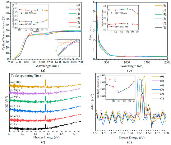
Figure 5.
Optical properties of the CIGS:Te thin films with different Te co-sputtering times of (1) 0, (2) 270, (3) 510, (4) 750, (5) 945, and (6) 1140 s. (a) Optical transmittance. The inset shows the mean optical transmittance in the visible and near-infrared (NIR) spectral regions. Magnitude of the optical transmittance in the visible spectral region is also shown in the inset. (b) Absorption coefficient. Mean absorbance in the visible and NIR spectral regions is shown in the inset. (c) The first derivative of absorbance as a function of incident photon energy for determination of the band gap. (d) Magnitude of the first derivative of absorbance spectrum. The inset shows the estimated band gap.
Hall-effect measurements were performed to analyze the electrical properties, including carrier concentration (n), carrier mobility (μ), and resistivity (ρ), of the CIGS:Te thin films, as shown in Figure 6. The electrical conductivity type of CIGS thin films can be influenced by various factors, including the ratio of In and Ga, Cu-deficiency, and the presence or absence of Se-excess during film fabrication. Neumann reported that the electrical conductivity type was determined by the deviations Δm and Δs [49], and Karthikeyan verified and further developed this relationship [28,45,50]. Hall-effect measurements showed n-type conductivity in the CIGS thin film without Te, with Δm < 0 and Δs < 0, as shown in Figure 6a and Figure 2d, which reported that CIS thin films with Δm < 0 always had n-type conductivity regardless of Δs in terms of the point defect model, and CIGS and CIAS thin films showed similar trends [29,51]. The electrical conductivity type dramatically changed the p-type conductivity in all CIGS:Te thin films, even though the thin films still showed deviations of Δm < 0 and Δs < 0, as shown in Figure 2d. The p-type conductivity of CIGS thin films is typically attributed to the formation of Cu vacancies and their interaction with Ga, which leads to the formation of a p-type defect complex [52]. The influence of the ratio of In and Ga is well known that CIGS thin films with a higher Ga content tend to have a higher hole concentration and therefore p-type conductivity. The CIGS thin films prepared under Se-excess exhibit p-type conductivity, whereas the thin films prepared under Se-deficiency exhibit n-type conductivity [53]. However, the same Cu-deficient target was used in all conditions of this study; so, the relative atomic percentage of In, Ga, and Se, and the composition ratio of Ga/(In + Ga) were nearly constant across all conditions (Figure 2b,c). Therefore, this is because of the surplus In + Ga atoms (Figure 2e), indicating the presence of positive ions in the crystal. The electrical conductivity types exhibited different behaviors because of the thin films with larger Δm and Δs in this study, and the electrical conductivity types with larger Δm and Δs could not be determined in terms of the point defect model [49]. Generally, electrical conductivity is sensitive to multiscale defect scattering carriers, including dislocations, pores, grain boundaries, and point defects in thin films [22,54]. Point defects, which can be formed by growth conditions, directly affect the electrical conductivity of the thin films. Figure 6a shows that the carrier concentrations were on the order of 1020−1021 cm−3 under all conditions. Among the CIGS:Te thin films co-sputtered with Te to the CIGS thin film, the two conditions of (2) and (6) with relatively high carrier concentrations were consistent with the conditions with poor surface properties in Figure 1. A higher carrier concentration was inferred to be caused by higher potential barriers that originated from small crystallites with larger imperfections [51,55]. This is because under condition (6), the CIGS:Te thin films have the highest In + Ga surplus and the largest Se + Te vacancies, resulting in the largest number of defects and, as a result, the highest carrier concentration, whereas under condition (3), with the closest stoichiometry, the CIGS:Te thin films show the smallest number of defects and, as a result, the smallest carrier concentration. This is also consistent with the conditions under which the microstrain and dislocation density are high, as shown in Figure 4c. The carrier mobility is on the order of 10−1 cm2/V∙s, as shown in Figure 6a, which is similar to or slightly higher than previously reported values for CIGS thin films owing to the replacement of Se vacancies by Te, which do not act as point defects or impurities. The carrier mobility under conditions (2) and (6) decreases suddenly because the large gaps interfere with the carrier’s movement from a grain to its neighboring grain. After Te co-sputtering, the resistivity generally decreases to the range of 10−2–10−1 Ω∙cm. Resistivity in the thin films depends mainly on the carrier concentration and mobility and obeys the relationship ρ = 1/nqµ. Under condition (4), a slight increase in resistivity was observed, which is correlated to lower carrier mobility with a consistent carrier concentration, that is, the number of imperfections.
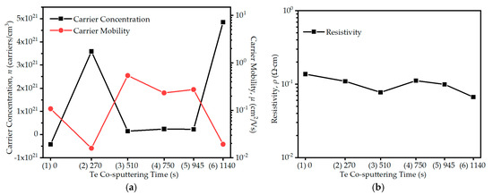
Figure 6.
(a) Carrier concentration (n), carrier mobility (μ), and (b) resistivity (ρ) in the CIGS:Te thin films with different Te co-sputtering times of (1) 0, (2) 270, (3) 510, (4) 750, (5) 945, and (6) 1140 s.
4. Conclusions
To solve the problems associated with the conventional selenization method of toxicity, high cost, and an environmentally unfriendly process for preparing an absorber layer of CIGS thin-film photovoltaics, several investigations were conducted on CIGS thin films fabricated through an annealing process after the sputtered precursors. However, even though the RTA process was performed, the thin-film properties were degraded because of the deterioration of crystallinity due to the lattice defects caused by the highly volatile Se. Therefore, the purpose of this study was to improve the crystallinity by compensating for the stoichiometry of the CIGS thin films through the RTA process after the co-sputtering of Te with CIGS. In the prepared CIGS:Te thin films, the compositional ratio did not increase linearly with the co-sputtering time, and the relative atomic ratio and compositional ratio of Te in the CIGS:Te thin films were small, and the amount of change was not large. However, significant changes were observed in the crystallinity in the XRD analysis and the surface properties in FESEM; when the deviation parameter (Δs) from the stoichiometry and normalized stoichiometric deviations were examined in this study, the results were largely consistent with the behaviors of thin-film properties. Under conditions where Δs was small and/or the normalized stoichiometric deviations of Se + Te and In + Ga were close to stoichiometric, the crystallinity of the CIGS:Te thin films was excellent, such as large grain size and clear grain boundaries, and the microstrain/dislocation density was the lowest, resulting in the largest volume of the unit cell. The optical properties of the CIGS:Te thin films as an absorber were also excellent compared to those of the CIGS thin film, with Eg = 1.548 eV. These were able to compensate for Se vacancies with appropriate co-sputtering of Te, which was confirmed through Hall-effect analysis to be the result of achieving the smallest number of defects while securing the best stoichiometry with the lowest carrier concentration (Se vacancies). Thus, the manufacturing improved-crystallinity CIGS:Te thin films without selenization using the proposed method can improve the efficiency of CIGS thin-film photovoltaics and advance their commercialization.
Supplementary Materials
The following supporting information can be downloaded at: https://www.mdpi.com/article/10.3390/app13074284/s1, Figure S1. (a) Schematic diagram of the co-sputtering deposition process with different Te co-sputtering times of (1) 0, (2) 270, (3) 510, (4) 750, (5) 945, and (6) 1140 s to prepare CIGS:Te thin films with a total thickness of 400 nm considering the deposition rates of Te and CIGS. All precursors were transferred to a rapid thermal annealing (RTA) system and subjected to heat treatment at 400 °C for 20 min under ambient N2. (b) Temperature–time profile of the RTA process for 20 min at 400 °C. Figure S2: Cross-sectional field emission scanning electron microscopy (FESEM) images of the CIGS:Te thin films with Te co-sputtering times of: (a) 0, (b) 270, (c) 510, (d) 750, (e) 945, and (f) 1140 s, corresponding to (a) 414, (b) 417, (c) 409, (d) 405, (e) 401, and (f) 397 nm, respectively. Note the different magnification of the images from (a).
Author Contributions
Conceptualization, S.P., Y.J.R. and N.-H.K.; investigation, S.P. and Y.J.R.; data curation, S.P., Y.J.R. and K.-Y.L.; writing—original draft preparation, S.P., Y.J.R. and S.K.; writing—review and editing, S.K., K.-Y.L. and N.-H.K.; project administration, N.-H.K.; funding acquisition, N.-H.K. All authors have read and agreed to the published version of the manuscript.
Funding
This study was supported by a research fund from Chosun University, 2022.
Institutional Review Board Statement
Not applicable.
Informed Consent Statement
Not applicable.
Data Availability Statement
Data are contained within the article or supplementary material.
Conflicts of Interest
The authors declare no conflict of interest. The founding sponsors had no role in the design of the study; in the collection, analyses, or interpretation of data; in the writing of the manuscript, or in the decision to publish the results.
References
- Atasoy, Y.; Başol, B.M.; Polat, İ.; Tomakin, M.; Parlak, M.; Bacaksız, E. Cu(In,Ga)(Se,Te)2 pentenary thin films formed by reaction of precursor layers. Thin Solid Films. 2015, 592, 189–194. [Google Scholar] [CrossRef]
- Kim, N.-H.; Jun, Y.-K.; Lee, W.-S. Co-Sputtered and Rapid-Thermal-Annealed CIAS Thin Films Using CuSe2/In/Al Triple Targets of Varying In/Al Compositions. J. Nanosci. Nanotechnol. 2016, 16, 1583–1586. [Google Scholar] [CrossRef] [PubMed]
- Teknetzi, I.; Holgersson, S.; Ebin, B. Valuable metal recycling from thin film CIGS solar cells by leaching under mild conditions. Sol. Energy Mater. Sol. Cells 2023, 252, 112178. [Google Scholar] [CrossRef]
- Huang, P.C.; Sung, C.C.; Chen, J.H.; Hsiao, R.C.; Hsu, C.Y. Effect of selenization and sulfurization on the structure and performance of CIGS solar cell. J. Mater. Sci. -Mater. Electron. 2018, 29, 1444–1450. [Google Scholar] [CrossRef]
- Za’abar, F.I.; Yusoff, Y.; Mohamed, H.; Abdullah, S.F.; Zuhdi, A.W.M.; Amin, N.; Chelvanathan, P.; Bahrudin, M.S.; Rahman, K.S.; Samsudin, N.A.; et al. A numerical investigation on the combined effects of MoSe2 interface layer and graded bandgap absorber in CIGS thin film solar cells. Coatings 2021, 11, 930. [Google Scholar] [CrossRef]
- Mabvuer, F.T.; Nya, F.T.; Kenfack, G.M.D.; Laref, A. Lowering Cost Approach for CIGS-Based Solar Cell Through Optimizing Band Gap Profile and Doping of Stacked Active Layers—SCAPS Modeling. ACS Omega 2023, 8, 3917–3928. [Google Scholar] [CrossRef]
- Kim, N.-H.; Oh, S.; Lee, W.S. Non-selenization method using sputtering deposition with a CuSe2 target for CIGS thin film. J. Korean Phys. Soc. 2012, 61, 1177–1180. [Google Scholar] [CrossRef]
- Lin, Y.C.; Lin, Z.Q.; Shen, C.H.; Wang, L.Q.; Ha, C.T.; Peng, C. Cu(In,Ga)Se2 films prepared by sputtering with a chalcopyrite Cu(In,Ga)Se2 quaternary alloy and In targets. J. Mater. Sci. -Mater. Electron. 2011, 23, 493–500. [Google Scholar] [CrossRef]
- Yu, S.; Jiang, J.; Han, S.; Hao, S.; Zhu, Q.; Gong, Y.; Yan, W.; Huang, W.; Xin, H. Structure engineering of solution-processed precursor films for low temperature fabrication of CuIn(S,Se)2 solar cells. Sol. Energy 2021, 220, 796–801. [Google Scholar] [CrossRef]
- Jheng, B.T.; Liu, P.T.; Wu, M.C.; Shieh, H.P. A non-selenization technology by co-sputtering deposition for solar cell applications. Opt. Lett. 2012, 37, 2760–2762. [Google Scholar] [CrossRef]
- Oh, S.; Kim, N.-H. Cigs Thin Films Sputtered by Using Chalcogenide Cuse2 With Multilayer-Stack-Structure and Rapid Thermal Annealing. Chalcogenide Lett. 2014, 11, 71–77. Available online: http://www.chalcogen.ro/71_Oh.pdf (accessed on 27 February 2023).
- Bouchama, I.; Djessas, K.; Saeed, M.A. Physical properties of CuIn0.7Ga0.3Se2 ingot and thin films prepared by one-step rf-magnetron sputtering from single-target material. J. Mol. Struct. 2020, 1217, 128457. [Google Scholar] [CrossRef]
- Kim, N.-H.; Jun, Y.K.; Cho, G.B. Se-loss-induced CIS Thin Films in RTA Process after Co-sputtering Using CuSe2 and InSe2 Targets. J. Electr. Eng. Technol. 2014, 9, 1009–1015. [Google Scholar] [CrossRef]
- Bouabid, K.; Ihlal, A.; Manar, A.; Outzourhit, A.; Ameziane, E.L. Effect of deposition and annealing parameters on the properties of electrodeposited CuIn1− xGaxSe2 thin films. Thin Solid Films. 2005, 488, 62–67. [Google Scholar] [CrossRef]
- Ahmed, E.; Zegadi, A.; Hill, A.E.; Pilkington, R.D.; Tomlinson, R.D.; Dost, A.A.; Ahmed, W.; Leppävuori, S.; Levoska, J.; Kusmartseva, O. The influence of annealing processes on the structural, compositional and electro-optical properties of CuIn0.75Ga0.25Se2 thin films. J. Mater. Sci.-Mater. Electron. 1996, 7, 213–219. [Google Scholar] [CrossRef]
- Do, Q.; Manh, N.T.; Triet, L.N.D.; Choi, Y.; Lee, Y.-W.; Cho, Y.; Lee, K.J.; Cho, N. Controlling the morphology of solution-processed CuIn(SSe)2 absorber layers by film thickness and annealing temperature. Mol. Cryst. Liquid Cryst. 2020, 707, 126–139. [Google Scholar] [CrossRef]
- Desarada, S.V.; Chavan, K.B.; Chaure, N.B. Effect of Different Annealing Techniques on CIGS Deposited Using One-Step Single-Target Sputtering. J. Electron. Mater. 2023, 1–7. [Google Scholar] [CrossRef]
- Singh, H.; Bharti, A.; Kumar, A.; Goyal, N.; Gill, P.S. Crystal Structure Characterization and Morphology of Tellurium Doped Multicomponent Chalcogenide Copper Indium Gallium Diselenide Compound. Mater. Focus 2017, 6, 611–617. [Google Scholar] [CrossRef]
- Fiat, S.; Koralli, P.; Bacaksiz, E.M.; Giannakopoulos, K.P.; Kompitsas, M.; Manolakos, D.E.; Çankaya, G.Ü. The influence of stoichiometry and annealing temperature on the properties of CuIn0. 7Ga0.3Se2 and CuIn0.7Ga0.3Te2 thin films. Thin Solid Films 2013, 545, 64–70. [Google Scholar] [CrossRef]
- Singh, U.P.; Shafarman, W.N.; Birkmire, R.W. Surface sulfurization studies of Cu(InGa)Se2 thin film. Sol. Energy Mater. Sol. Cells 2006, 90, 623–630. [Google Scholar] [CrossRef]
- Kim, S.; Kim, N.-H. Impurity phases and optoelectronic properties of CuSbSe2 thin films prepared by cosputtering process for absorber layer in solar cells. Coatings 2020, 10, 1209. [Google Scholar] [CrossRef]
- Oh, S.; Park, Y.S.; Ko, P.J.; Kim, N.-H. Effects of rapid thermal treatment on properties of magnetron-sputtered NiO thin films for supercapacitor applications. J. Nanosci. Nanotechnol. 2018, 18, 6213–6219. [Google Scholar] [CrossRef] [PubMed]
- Khosroshahi, R.; Dehghani, M.; Tehrani, N.A.; Taghavinia, N.; Bagherzadeh, M. Optimization of selenization process to remove Ga-induced pin-holes in CIGS thin films. Sol. Energy 2022, 236, 175–181. [Google Scholar] [CrossRef]
- Pech, S.; Kim, S.; Kim, N.-H. Magnetron Sputter-Deposited β-Ga2O3 Films on c-Sapphire Substrate: Effect of Rapid Thermal Annealing Temperature on Crystalline Quality. Coatings 2022, 12, 140. [Google Scholar] [CrossRef]
- Erkan, S.; Başol, B.M.; Atasoy, Y.A.; Çiriş, A.; Yüksel, Ö.F.; Bacaksız, E. Cu(In,Ga)Te2 film growth by a two-stage technique utilizing rapid thermal processing. Semicond. Sci. Technol. 2019, 34, 035011. [Google Scholar] [CrossRef]
- Atasoy, Y.; Başol, B.M.; Olğar, M.A.; Tomakin, M.U.; Bacaksız, E. Cu(In,Ga)(Se,Te)2 films formed on metal foil substrates by a two-stage process employing electrodeposition and evaporation. Thin Solid Films 2018, 649, 30–37. [Google Scholar] [CrossRef]
- Kim, N.-H.; Sung, B.S.; Jun, Y.K.; Chung, D.H.; Lee, W.S. Low-temperature, rapid thermal annealing of CIS thin films deposited by using a co-sputtering process with in and CuSe2 targets. J. Korean Phys. Soc. 2015, 66, 1001–1008. [Google Scholar] [CrossRef]
- Karthikeyan, S.; Hill, A.E.; Pilkington, R.D.; Cowpe, J.S.; Hisek, J.; Bagnall, D.M. Single step deposition method for nearly stoichiometric CuInSe2 thin films. Thin Solid Films 2011, 519, 3107–3112. [Google Scholar] [CrossRef]
- Wu, S.; Zhou, L.; Wang, Y.; Xue, Y.; Teng, Y. Effect of Al content on the performance of Cu(In,Al)Se2 powders prepared by mechanochemical process. Mater. Sci. Semicond. Process 2014, 18, 128–134. [Google Scholar] [CrossRef]
- Boonlakhorn, J.; Prachamon, J.; Manyam, J.; Krongsuk, S.; Thongbai, P.; Srepusharawoot, P. Colossal dielectric permittivity, reduced loss tangent and the microstructure of Ca1−xCdxCu3Ti4O12−2yF2y ceramics. RSC Adv. 2021, 11, 16396–16403. [Google Scholar] [CrossRef]
- Shokeen, P.; Jain, A.; Kapoor, A.; Gupta, V. Thickness and Annealing Effects on the Particle Size of PLD Grown Ag Nanofilms. Plasmonics 2016, 11, 669–675. [Google Scholar] [CrossRef]
- Wang, C.-J.; Shei, S.-C.; Chang, S.-J. Novel solution process for synthesis of CIGS nanoparticles using polyetheramine as solvent. Mater. Lett. 2014, 122, 52–54. [Google Scholar] [CrossRef]
- Islam, M.A.; Huda, Q.; Hossain, M.S.; Aliyu, M.M.; Karim, M.R.; Sopian, K.; Amin, N. High quality 1 μm thick CdTe absorber layers grown by magnetron sputtering for solar cell application. Curr. Appl. Phys. 2013, 13, S115–S121. [Google Scholar] [CrossRef]
- Hao, S.; Yu, S.; Liu, X.; Li, B.; Han, S.; Xin, H.; Yan, W.; Huang, W. Effect of K Doping on the Performance of Aqueous Solution-Processed Cu(In,Ga)Se2 Solar Cell. Adv. Energy Sustain. Res. 2022, 3, 2200006. [Google Scholar] [CrossRef]
- Kumar, S.; Asokan, K.; Singh, R.K.; Chatterjee, S.; Kanjilal, D.; Ghosh, A.K. Investigations on structural and optical properties of ZnO and ZnO: Co nanoparticles under dense electronic excitations. RSC Adv. 2014, 4, 62123–62131. [Google Scholar] [CrossRef]
- Kim, N.H.; Yoo, M.H.; Ko, P.J.; Lee, W.S. Deviations from stoichiometry and molecularity in non-stoichiometric Ag-In-Se thin films: Effects on the optical and the electrical properties. J. Korean Phys. Soc. 2016, 69, 1817–1823. [Google Scholar] [CrossRef]
- Marai, A.B.; Belgacem, J.B.; Ayadi, J.B.; Djessas, K.; Alaya, S. Structural and optical properties of CuIn1-xGaxSe2 nanoparticles synthesized by solvothermal route. J. Alloys Compd. 2016, 658, 961–966. [Google Scholar] [CrossRef]
- Goh, K.H.; Haseeb, A.S.M.A.; Wong, Y.H. Physical and electrical properties of thermal oxidized Sm2O3 gate oxide thin film on Si substrate: Influence of oxidation durations. Thin Solid Films 2016, 606, 80–86. [Google Scholar] [CrossRef]
- Rabiei, M.; Palevicius, A.; Monshi, A.; Nasiri, S.; Vilkauskas, A.; Janusas, G. Comparing Methods for Calculating Nano Crystal Size of Natural Hydroxyapatite Using X-ray Diffraction. Nanomaterials 2020, 10, 1627. [Google Scholar] [CrossRef]
- Khallaf, H.; Chai, G.; Lupan, O.; Chow, L.; Park, S.; Schulte, A. Characterization of gallium-doped CdS thin films grown by chemical bath deposition. Appl. Surf. Sci. 2009, 255, 4129–4134. [Google Scholar] [CrossRef]
- Reddy, D.S.; Rao, K.N.; Gunasekhar, K.R.; Reddy, N.K.; Kumar, K.S.; Reddy, P.S. Annealing effect on structural and electrical properties of thermally evaporated Cd1−xMnxS nanocrystalline films. Mater. Res. Bull. 2008, 43, 3245–3251. [Google Scholar] [CrossRef]
- Gu, Y.; Li, X.; Yu, W.; Gao, X.; Zhao, J.; Yang, C. Microstructures, electrical and optical characteristics of ZnO thin films by oxygen plasma-assisted pulsed laser deposition. J. Cryst. Growth 2007, 305, 36–39. [Google Scholar] [CrossRef]
- Chandramohan, S.; Sathyamoorthy, R.; Sudhagar, P.; Kanjilal, D.; Kabiraj, D.; Asokan, K. Optical properties of swift ion beam irradiated CdTe thin films. Thin Solid Films 2008, 516, 5508–5512. [Google Scholar] [CrossRef]
- Sathyamoorthy, R.; Narayandass, S.K.; Mangalaraj, D. Effect of substrate temperature on the structure and optical properties of CdTe thin film. Sol. Energy Mater. Sol. Cells 2003, 76, 339–346. [Google Scholar] [CrossRef]
- Oh, M.S.; Hwang, D.K.; Seong, D.J.; Hwang, H.S.; Park, S.J.; Kim, E.D. Improvement of characteristics of Ga-doped ZnO grown by pulsed laser deposition using plasma-enhanced oxygen radicals. J. Electrochem. Soc. 2008, 155, D599. [Google Scholar] [CrossRef]
- Nicolaou, C.; Zacharia, A.; Delimitis, A.; Itskos, G.; Giapintzakis, J. Single-step growth of high quality CIGS/CdS heterojunctions using pulsed laser deposition. Appl. Surf. Sci. 2020, 511, 145547. [Google Scholar] [CrossRef]
- Mansour, A.M.; Nasr, M.; Saleh, H.A.; Mahmoud, G.M. Physical characterization of 5′,5″-dibromo-o-cresolsulfophthalein (BCP) spin-coated thin films and BCP/p-Si based diode. Appl. Phys. A-Mater. Sci. Process. 2019, 125, 625. [Google Scholar] [CrossRef]
- Kodalle, T.; Greiner, D.; Brackmann, V.; Prietzel, K.; Scheu, A.; Bertram, T.; Reyes-Figueroa, P.; Unold, T.; Abou-Ras, D.; Schlatmann, R.; et al. Glow discharge optical emission spectrometry for quantitative depth profiling of CIGS thin-films. J. Anal. At. Spectrom. 2019, 34, 1233–1241. [Google Scholar] [CrossRef]
- Neumann, H.; Tomlinson, R.D. Relation between electrical properties and composition in CuInSe2 single crystals. Sol. Cells 1990, 28, 301–313. [Google Scholar] [CrossRef]
- Müller, J.; Nowoczin, J.; Schmitt, H. Composition, structure and optical properties of sputtered thin films of CuInSe2. Thin Solid Films 2006, 496, 364–370. [Google Scholar] [CrossRef]
- Kim, N.H.; Ko, P.J.; Cho, G.B.; Park, C.I. Rapid laser annealing of Cu(In,Ga)Se2 thin films by using a continuous wave Nd:YAG laser (λ0 = 532 nm). J. Korean Phys. Soc. 2017, 70, 809–815. [Google Scholar] [CrossRef]
- Suresh, S.; Rokke, D.J.; Drew, A.A.; Alruqobah, E.; Agrawal, R.; Uhl, A.R. Extrinsic Doping of Ink-Based Cu(In,Ga)(S,Se)2-Absorbers for Photovoltaic Applications. Adv. Energy Mater. 2022, 12, 2103961. [Google Scholar] [CrossRef]
- Ou, C.Y.; Som, S.; Lu, C.H.; Gupta, K.K.; Chaurasiya, R. Photovoltaic characteristics and computational simulation of samarium-ion doped Cu(In, Ga)Se2 thin films prepared via a non-vacuum coating process. J. Alloys Compd. 2021, 881, 160377. [Google Scholar] [CrossRef]
- Qiao, J.; Zhao, Y.; Jin, Q.; Tan, J.; Kang, S.; Qiu, J.; Tai, K. Tailoring nanoporous structures in Bi2Te3 thin films for improved thermoelectric performance. ACS Appl. Mater. Interfaces 2019, 11, 38075–38083. [Google Scholar] [CrossRef]
- Shinde, U.P. Hall coefficient, mobility and carrier concentration as a function of composition and thickness of Zn-Te thin films. Adv. Appl. Sci. Res. 2015, 4, 215–220. Available online: https://api.semanticscholar.org/CorpusID:55769927 (accessed on 27 February 2023).
Disclaimer/Publisher’s Note: The statements, opinions and data contained in all publications are solely those of the individual author(s) and contributor(s) and not of MDPI and/or the editor(s). MDPI and/or the editor(s) disclaim responsibility for any injury to people or property resulting from any ideas, methods, instructions or products referred to in the content. |
© 2023 by the authors. Licensee MDPI, Basel, Switzerland. This article is an open access article distributed under the terms and conditions of the Creative Commons Attribution (CC BY) license (https://creativecommons.org/licenses/by/4.0/).