1. Introduction
The creation of compact, coherent radiation sources in the terahertz frequency range (0.1–10 THz) operating at room temperature and also having high sensitivity and speed is of great practical interest [
1,
2]. This interest is caused by the possibilities of their wide application in various fields such as medicine, meteorology, security systems, wireless high-speed communications, spectroscopy, etc. [
2,
3].
The terahertz frequency range lies between long-wave infrared radiation and ultrahigh-frequency millimeter waves. Therefore, scientific research in the fields of electronics and photonics is carried out to create devices operating in this frequency range. Among electronic devices for generating terahertz radiation, Gunn diodes, high electron mobility transistors (HEMs), impact ionization avalanche transit-time diodes (IMPATTs), and tunnel injection transit-time negative resistance diodes (TUNNETTs) are usually considered; quantum cascade lasers (QCLs) are popular among optical devices [
3].
One of the possible candidates as a source of terahertz radiation is a resonant tunneling diode (RTD) related to solid-state, compact electronic devices operating at room temperature. For the first time, the generation of electromagnetic radiation on an RTD was obtained at a temperature of about 200 K in 1984 [
4], while the frequency and output power were small and amounted to 18 GHz and several
W, respectively. Subsequently, by reducing the thickness of the quantum well and barriers [
5] and optimizing the thickness of the collector spacer [
6] and the size of the slot antenna [
7], it was possible to achieve a significant increase in the oscillation frequency. At the moment, the oscillation frequency of RTDs of the order of 2 THz has been experimentally obtained [
8,
9,
10], which is a record for electronic devices operating at room temperature.
Despite the recent obvious progress in the frequency characteristics of the resonant tunnel diode, the generation power in the terahertz frequency range remains small (about 1
W). In this regard, theoretical studies aimed at a deeper physical understanding of various features of resonant tunneling processes in nanostructures acquire an important role. Detailed theoretical studies of RTDs, carried out earlier [
11,
12,
13,
14,
15,
16,
17], made it possible to make significant progress in understanding the resonant tunneling processes in a constant and alternating high-frequency electric field. However, these studies did not take into account the important features inherent in experimental structures, such as the charge accumulation effects, the presence of spacer layers, and the highly doped contacts in the structure, so they can only serve as a reference point for further research.
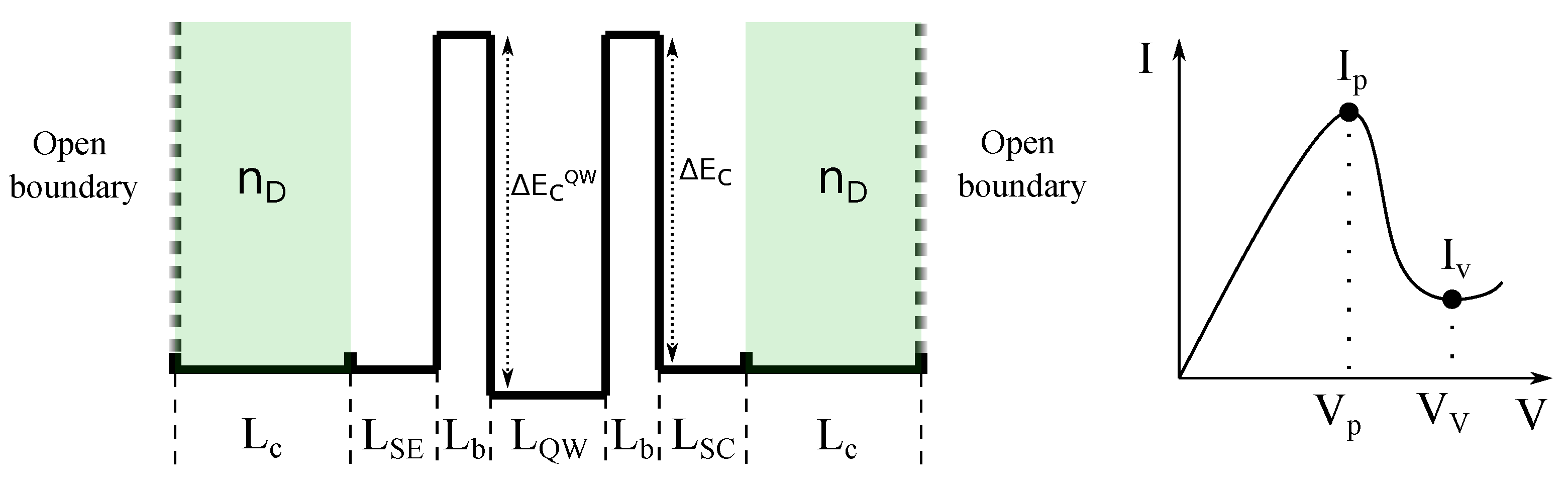
The parameters of the active region (quantum well and barriers) represent the main importance in controlling the characteristics of resonant tunneling diodes since they determine the width and energy of the resonant levels. Spacer layers, which are located between the active region and the doped contact areas, also have a great influence on the processes of resonant tunneling (see
Figure 1). Initially, spacer layers were used to reduce the diffusion of donor impurities into the undoped active region. However, it turned out that the role of spacer layers is not limited to this application, and they may have a significant impact on both the static and dynamic characteristics of the resonant tunneling diodes.
Experimental studies of the effect of spacer layers on the static characteristics of RTDs were carried out in [
18,
19,
20,
21,
22]. The attention was mainly paid to the influence of the thickness of the spacer layers on the peak and valley currents. In [
18], an InGaAs-/InAs-based structure demonstrated that the peak and valley currents decrease with the increasing thickness of the spacer layers (the thickness of the emitter and collector spacers together varies within 1 and 5 nm). In [
19], the data for three values of the thickness of spacer layers
=
= 15, 30, 60 nm for an AlGaAs/GaAs structure was demonstrated, and it was shown that the peak current remains constant. However, the results of [
19] did not address the important region of small spacer layer thicknesses < 15 nm, and the spacer thickness step was also rather large, which does not allow one to correctly identify the possible features of the dependence of the peak current on the spacer thickness. In [
20], it was demonstrated for the AlGaAs/GaAs structure that a change in the emitter spacer thickness leads to a decrease in the peak current and valley current, while a change in the collector spacer thickness keeps these static characteristics constant. In [
21] for a AlGaAs/GaAs resonant tunneling nanostructure, the peak current dependence was obtained for large thicknesses of the emitter spacer (<20 nm). The maximum value of the peak current was reached at the smallest considered thickness of the emitter spacer
= 20 nm, then the peak current decreased and remained constant with a further increase in the thickness of the emitter spacer. Thus, experimental works usually consider a limited set of several spacer layer thicknesses for the chosen configuration of the RTD active region. Moreover, a number of studies considered simultaneous changes in the thickness of the emitter spacer and the collector spacer [
18,
19]. Often, studies are carried out for sufficiently large thicknesses of spacer layers > 15 nm with a large thickness step (>15 nm) [
19,
20]. This does not allow one to establish the influence of each of the spacers separately and draw some generalized conclusions about the functional dependences of important static characteristics (peak current, valley current, etc.) on the thickness of the spacer layers.
In [
11,
12], using a numerical solution of the Schrodinger equation with open boundary conditions, it was shown that the dependence of the peak current on the emitter spacer thickness has an oscillating character. Moreover, the peak current takes the smallest value at small spacer thicknesses. The peak current reaches its maximum value at the emitter spacer thicknesses at which the resonant level in the quantum well overlaps with the energy level that occurs in the triangular well of the emitter spacer, which is formed when a constant voltage is applied [
11,
12]. For the RTD structure considered in [
11,
12], due to the correct choice of the emitter spacer thickness, it was possible to achieve peak current amplification by about six-times compared to the case of the absence of a spacer. However, the results in [
11,
12] were obtained in a simplified formulation of the problem, which did not take into account the effects of charge accumulation (i.e., the approximation of non-interacting electrons was used), as well as the presence of highly doped contact regions.
In this study, the effect of the emitter and collector spacer thickness on the main static characteristics, such as the peak current (), valley current (), and corresponding applied voltages ( and ), of resonant tunneling nanostructures, was studied, taking into account the effects of charge accumulation and the presence of highly doped contact regions.
2. Materials and Methods
In the present study, we considered two-barrier resonant tunneling nanostructures. Schematically, the potential profile of the bottom of the conduction band of such a structure is shown in
Figure 1. Electrons distributed by energies according to the Fermi–Dirac statistics are injected into the structure from contacts located to the left and right of the active region. We assumed that the transport of charge carriers is ballistic. We considered the model that takes into account the presence of highly doped contact regions (in
Figure 1, these regions are highlighted in green and have a thickness of
and a donor concentration of
), as well as undoped spacer layers that prevent the penetration of impurities into the active quantum region. The thickness of the emitter spacer is denoted by
, and the thickness of the collector spacer is
. The active region of the resonant tunneling nanostructure is formed by the two potential barriers with a thickness of
and a height of
, between which the quantum well with the thickness of
is located.
Calculations of the electronic transport through the resonant tunneling nanostructures within the framework of the numerical solution of the stationary system of Schrodinger–Poisson equations taking into account spacer layers and strongly doped contact regions face divergence problems partially described in [
23]. Our study showed that all the methods proposed so far allow us to achieve the convergence of the solution only in a limited range of structure parameters. For structures with small values of the resonance-level width (for example, as for the structure considered in [
23,
24]), the divergence of the numerical solution is observed at emitter spacer thicknesses less than 6 nm. For structures with large values of the resonance-level width (for example, the structures from [
25,
26]), the minimum thickness of the emitter spacer, at which there is no divergence of the numerical solution of the stationary problem, increases. Thus, the thicknesses of spacer layers less than 8–10 nm are inaccessible for analysis in the framework of a stationary formulation of the problem, although such thicknesses are used in experimental structures [
25,
26]. A possible reason for the divergence of the numerical solution of the stationary problem may be the poor fulfillment of the electroneutrality condition.
To calculate the static current–voltage characteristics, we developed a technique based on the numerical solution of the open time-dependent Schrodinger–Poisson equations:
a set of Schrodinger equations with different values of the wave vectors
k is solved;
is the potential of the time-dependent electric field;
is the self-consistent potential in the Hartree approximation;
is the electron density;
is the Fermi–Dirac distribution integrated along the transverse wave vector;
T is the temperature (all calculations were carried out for
K);
is the electron effective mass;
is the Fermi energy.
A detailed description of the difference scheme for solving the time-dependent Schrodinger–Poisson equations is given in [
23]. Exact discrete open boundary conditions for the Schrodinger equation are used to prevent the non-physical reflections from the boundaries of the computational domain [
23,
27,
28,
29].
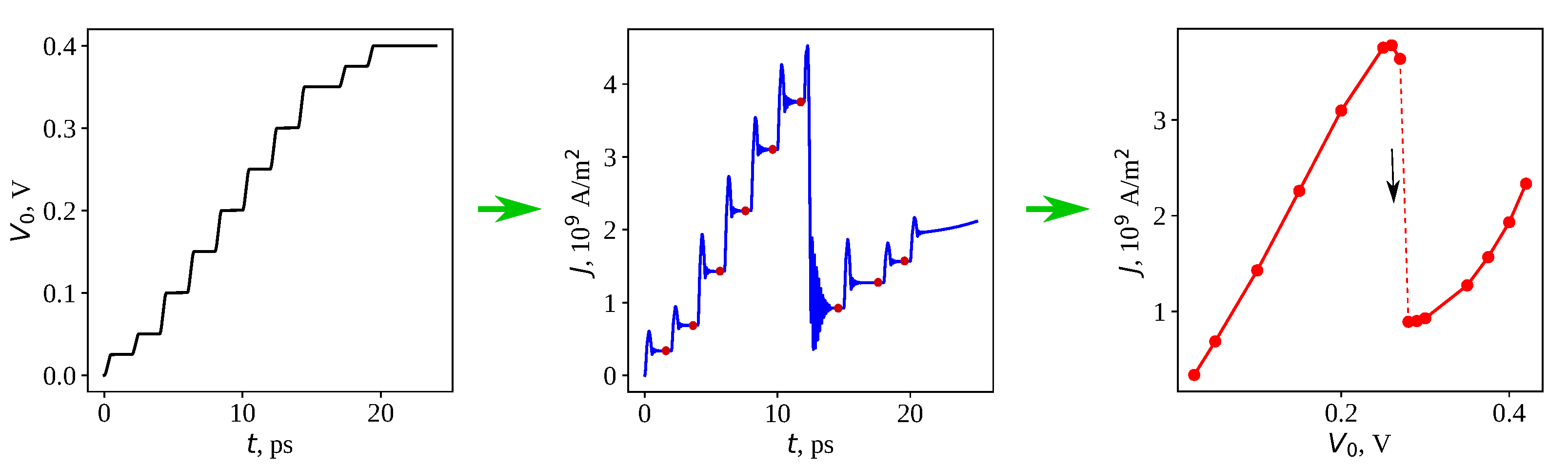
The main idea of the proposed approach to the calculation of the static characteristics of resonant tunneling nanostructures is illustrated in
Figure 2. The applied voltage
depends on the time. The voltage increase occurs in a stepwise manner. The time-constant voltage sections have a sufficient length to complete all transient processes. The current value established at this voltage is used for the subsequent construction of the current–voltage characteristic.
In the present study, the peak current value was optimized for the different values of the emitter spacer thickness. The determination of the peak current
is demonstrated in
Figure 1. The calculations were carried out for two structures that were previously studied in [
26,
30]: Structure #3, which differs from Structure #2 by replacing the quantum well material with In
Ga
As. The parameters of these structures are given in
Table 1.
3. Results and Discussion
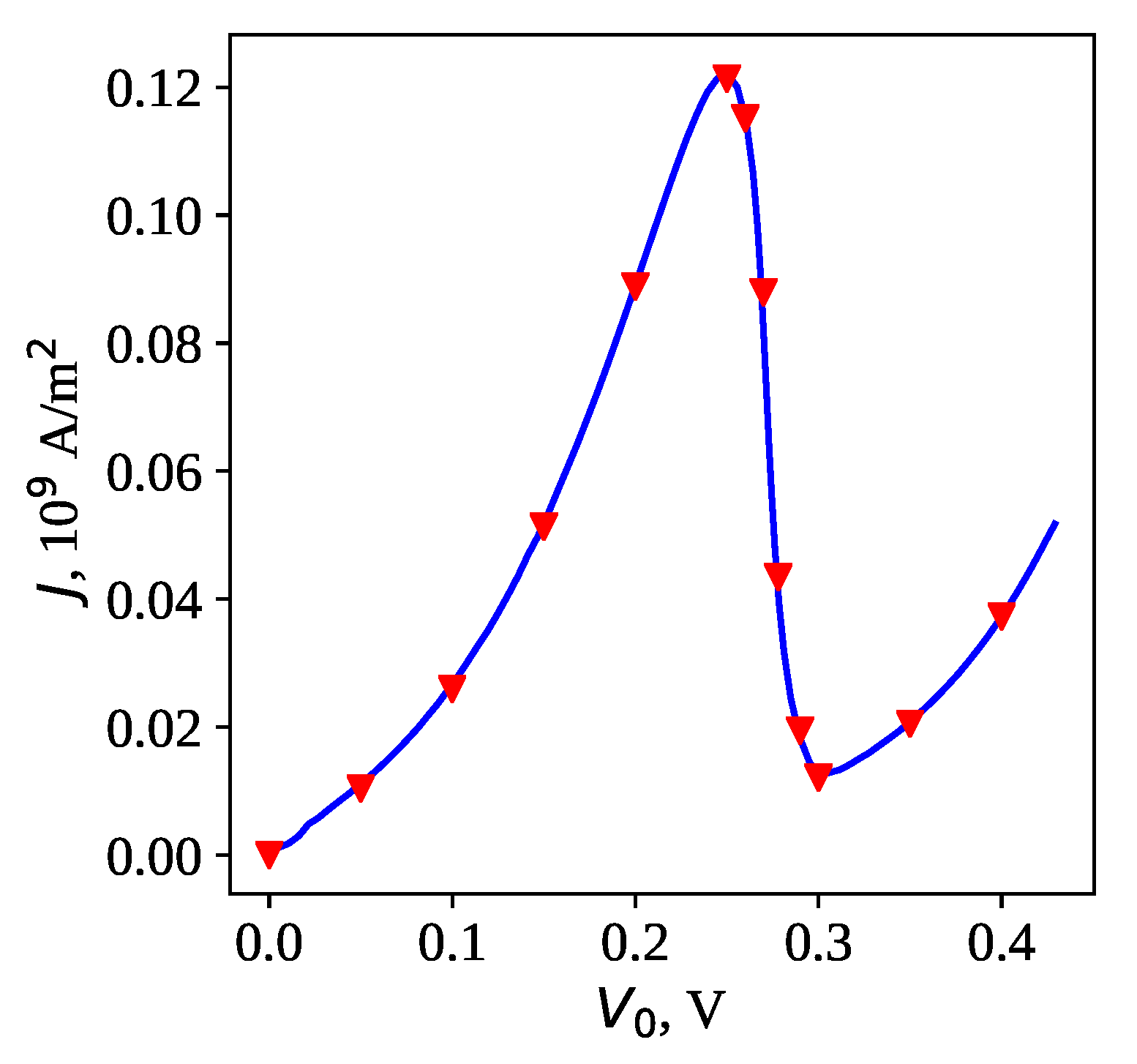
To verify the correctness of the developed methodology’s implementation, the calculations of the current–voltage characteristic for the structure from [
23] were carried out. Comparisons of the results from [
23] obtained in the framework of solving the stationary Schrodinger–Poisson problem are shown in
Figure 3. One can see that the current–voltage characteristic obtained in [
23] with a high degree of accuracy coincides with the results obtained using the methodology developed in the present study.
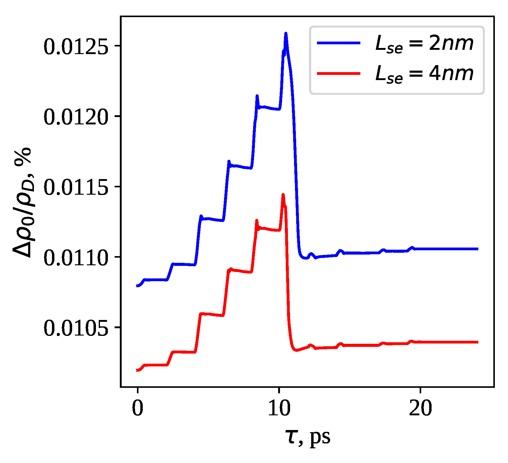
For the developed method of calculation based on the solution of the time-dependent Schrodinger–Poisson equations, the electroneutrality condition was fulfilled with a high degree of accuracy (with an error significantly less than 1%), which is demonstrated in
Figure 4 (the value
is postponed along the
y-axis).
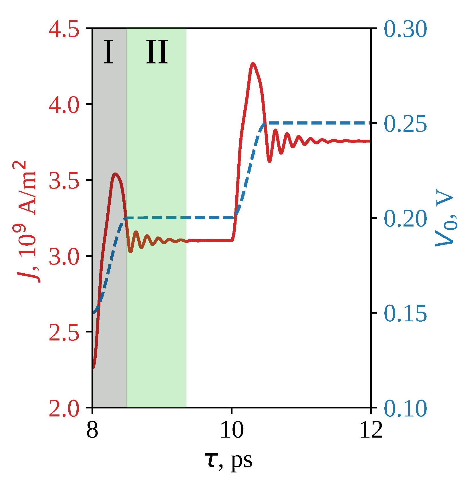
Due to the peculiarities of the calculation method proposed, along with the information obtained on the static characteristics of the considered resonant tunneling nanostructures, we also obtained the data for the analysis of transient processes under various conditions. The consideration of spacer layers and heavily doped contacts in the model of resonant tunneling nanostructures boils down to the fact that, at the beginning of the transition process (see Region I in
Figure 5), when the applied voltage increases rapidly over 0.5 ps, the nature of the transient process of resonant tunneling nanostructures corresponds to the behavior of the parallel plate capacitor [
23]. Then, the transition process associated with the restructuring of the state in the main quantum well begins (see Region II in
Figure 5). This transition process occurs over times of the order of the electron lifetime in the quantum well
(
—resonance-level width), which is consistent with the theoretical studies carried out earlier in the framework of the simplified model [
31,
32].
The change in the thickness of the emitter spacer has a weak effect on the transition times for all the structures considered. For Structure #1, the transition times to a new stationary state are approximately 1.3 ps, while for Structures #2 and #3, the transition times are approximately 0.9 ps. The difference in the transition times between Structure #1 and Structures #2 and #3 is because Structures #2 and #3 have smaller values of the thickness of the barrier layers, which leads to a greater value of the width of the resonance level, and consequently to a decrease in the transition time.
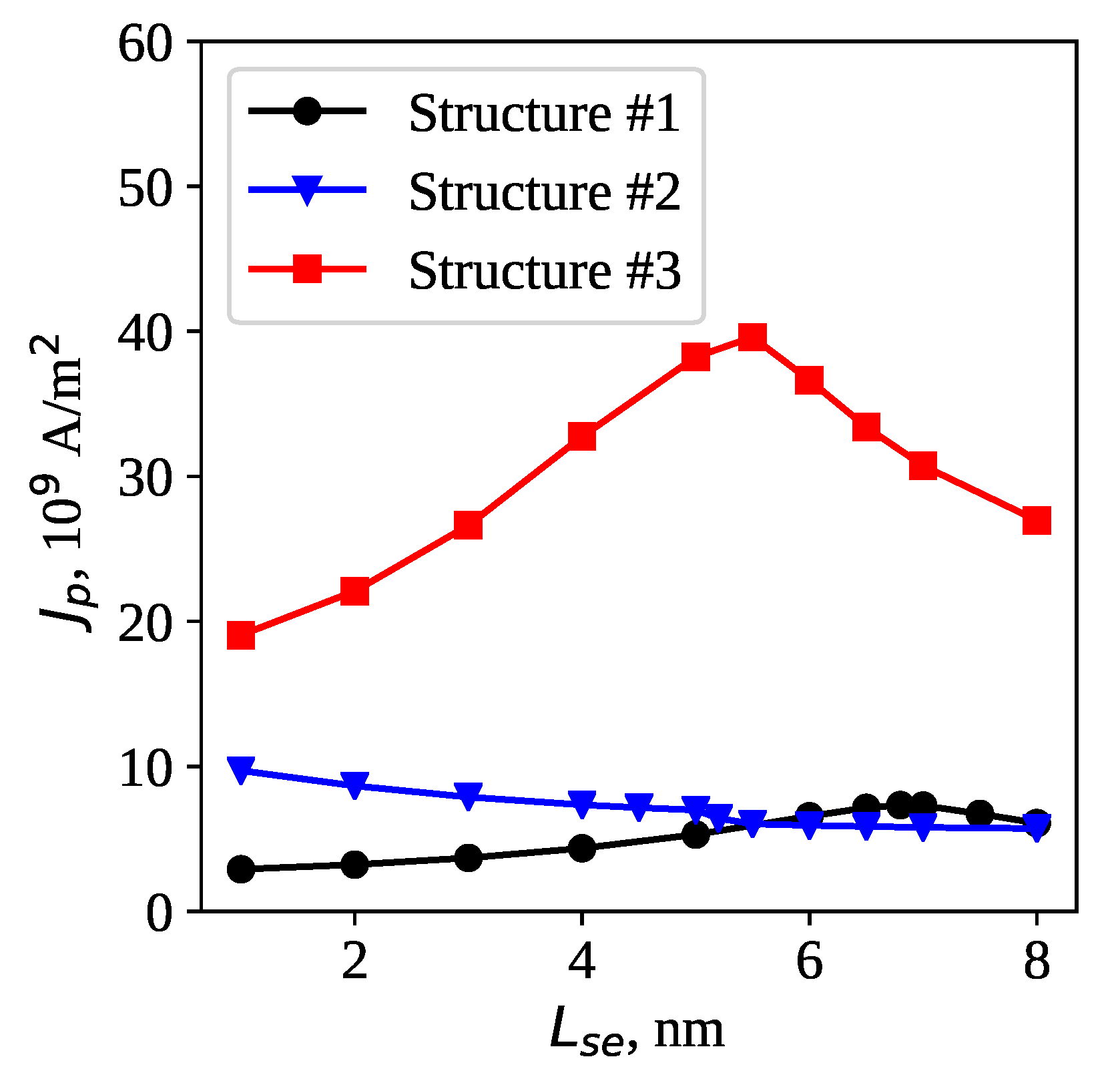
Let us consider the behavior of the peak current dependences on the thickness of the emitter spacer in the simplified model from [
11,
12], i.e., without taking into account the effects of charge accumulation (the self-consistent potential simulating interelectronic interaction is zero), as well as without taking into account the highly doped contact areas. The calculation results for the three resonant tunneling nanostructures are shown in
Figure 6. For Structures #1 and #3, the peak current maximum is observed at a certain value of the emitter spacer thickness (for Structure #1, it is 6.8 nm; for Structure #3, it is 5.5 nm). The increase in the peak current due to the optimization of the thickness of the emitter spacer compared to small spacer thicknesses for Structure #1 is approximately 2.4-times, and for Structure #3, it is 2-times. For Structure #2, the peak current decreases with the increasing thickness of the emitter spacer. The difference between Structures #2 and #3 is the use of the material with a smaller band gap in Structure #2 for a quantum well. This leads to a decrease in the energy of the resonance level in Structure #2, which makes it possible to reach peak current values at significantly lower values of the applied voltage. Thus, in the simplified model, without taking into account the effects of charge accumulation and heavily doped contact areas, the applied voltages at which the peak current value is reached are of the order of 0.15 eV for Structure #2 and the order of 0.7 eV for Structure #3. At the same time, in the considered range of changes in the thickness of the emitter spacer of 2–8 nm, Structure #2 has at least 2-times lower peak current values compared to Structure #3.
The current–voltage characteristics were calculated in our model at different values of the emitter spacer thickness in the range of 2–8 nm and the collector spacer thickness in the range of 3–18 nm for Structure #1 and in the range of 5–25 nm for Structures #2 and #3. The values of the peak current
, the valley current
, and the corresponding applied voltages
and
were determined from the obtained current–voltage characteristics. The results are presented in
Table 2 for Structure #1 and
Table 3 for Structures #2 and #3. The convergence problems of the numerical solution observed when solving the stationary Schrodinger–Poisson model were absent in our model in the considered range of the emitter spacer thickness.
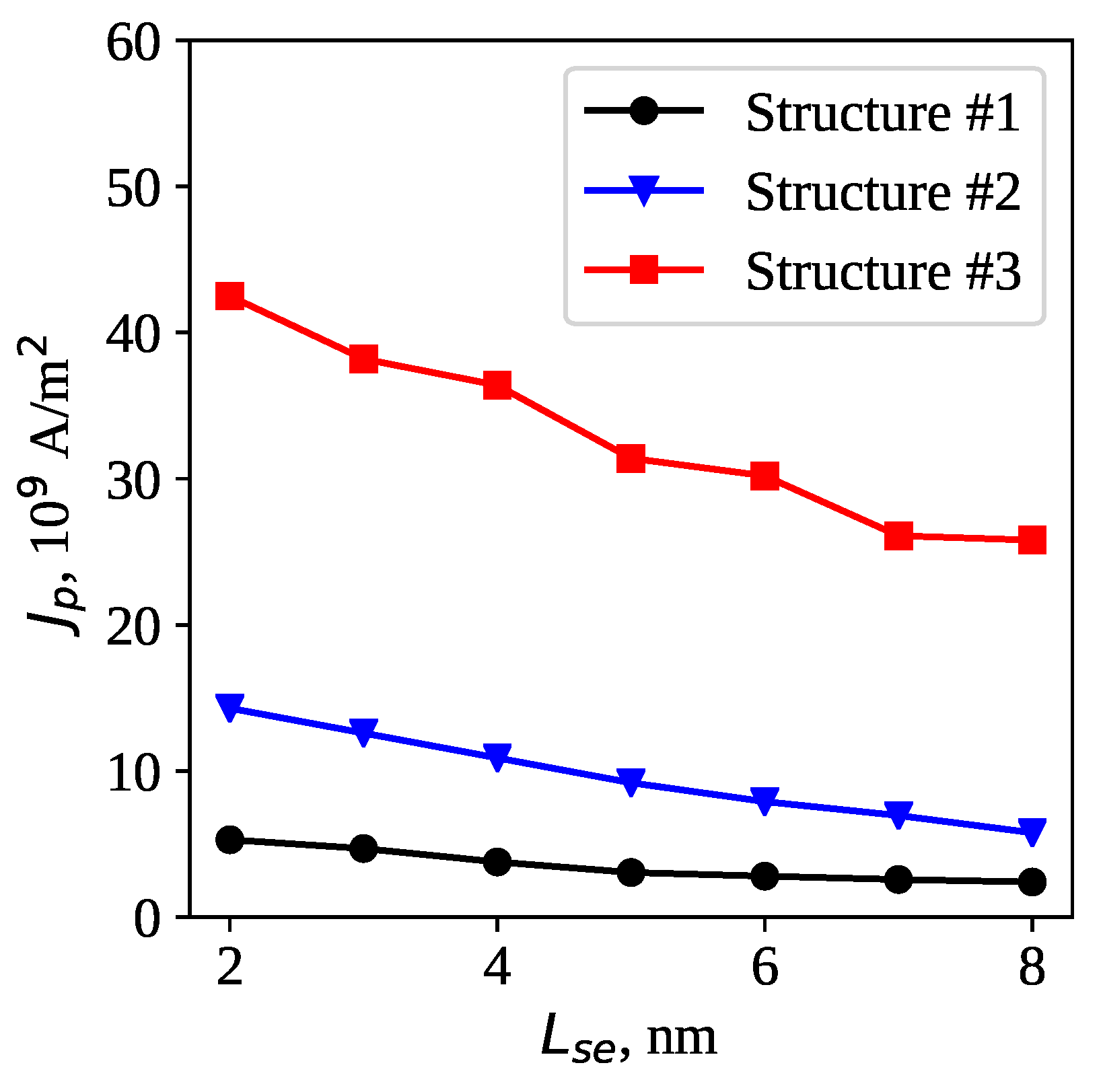
Figure 7 shows the dependence of the peak current on the thickness of the emitter spacer for the considered resonant tunneling nanostructures. Taking into account the effects of charge accumulation and heavily doped contact areas in the Schrodinger–Poisson model led to a radical change in the nature of the dependence of the peak current on the thickness of the emitter spacer for Structures #1 and #3. For these structures, an increase in the thickness of the emitter spacer was accompanied by a decrease in the peak current. For Structure #2, the peak current also decreased with increasing the thickness of the emitter spacer, i.e., a similar behavior was observed as in the calculations in the simplified model.
Thus, there was a discrepancy with the results of similar studies from [
11,
12]. The latter study predicted the existence of the optimal thickness of the emitter spacer at which the peak current of resonant tunneling nanostructures reaches the maximum value
. Moreover, the value of
significantly exceeded the value of the peak current at small thicknesses of the emitter spacer. When a voltage was applied to the structure, an additional triangular quantum well was formed in the region of the emitter spacer. The peak current increased significantly at such sizes of the additional quantum well, when the energy of the quasi-level in this well coincided with the energy of the resonant level in the main quantum well [
11,
12]. The calculations in [
11,
12] were carried out in the simplified formulation of the problem, which does not take into account the effects of charge accumulation and the presence of heavily doped contact regions. The consideration of these factors led to a significant modification of the triangular quantum well that occurs in the region of the emitter spacer in the presence of the applied voltage (see
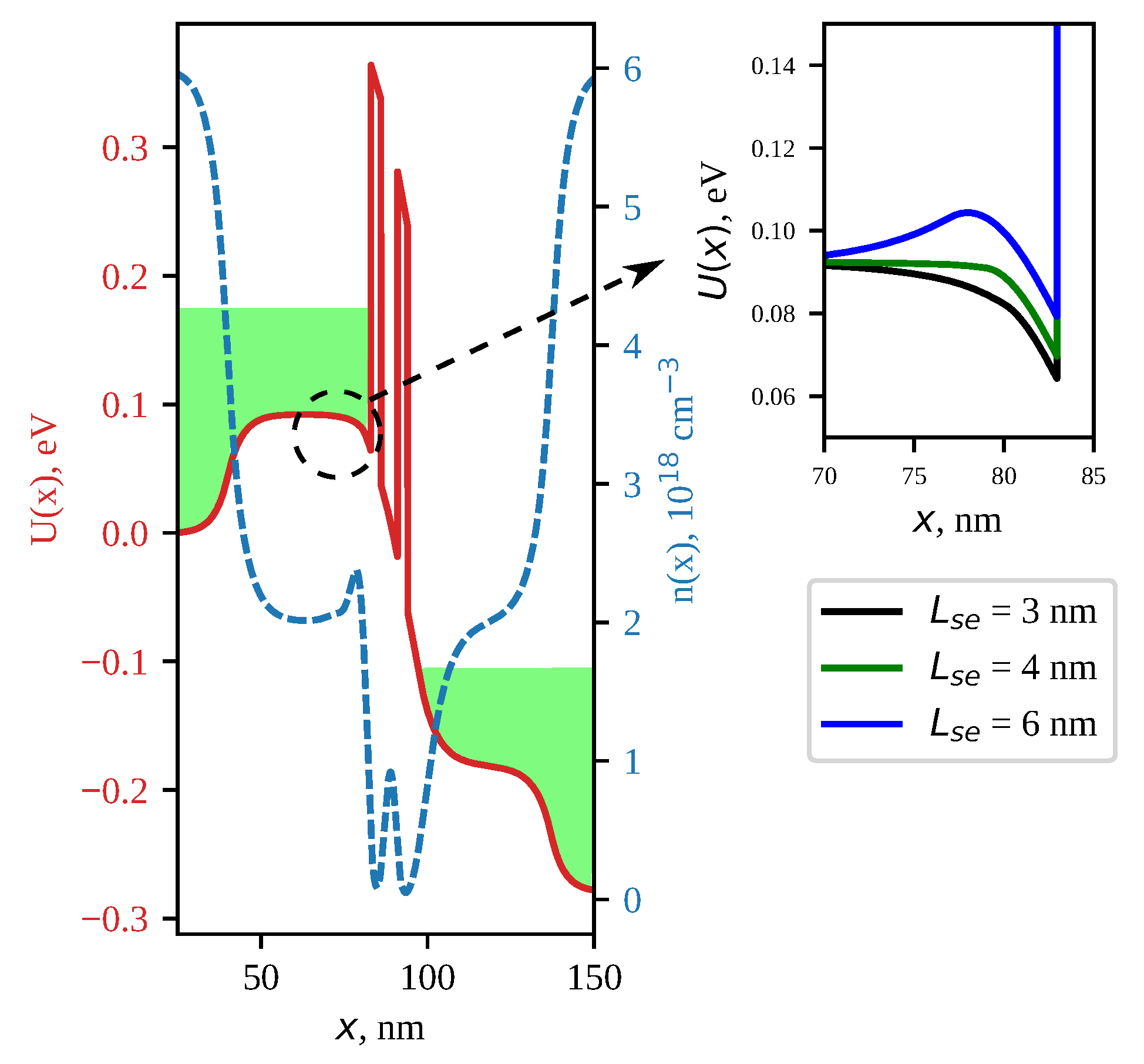
Figure 8). With an increase in the emitter spacer thickness, the size of the additional quantum well decreased, which led to a decrease in the peak current.
As can be seen from
Table 2 and
Table 3, with an increase in the thickness of the emitter spacer, the values of
,
, and
, as well as the value of
decreased for all the resonant tunneling nanostructures considered. The values of the applied voltage at which the current reached peak value
were significantly increased compared to the results obtained within the simplified model.
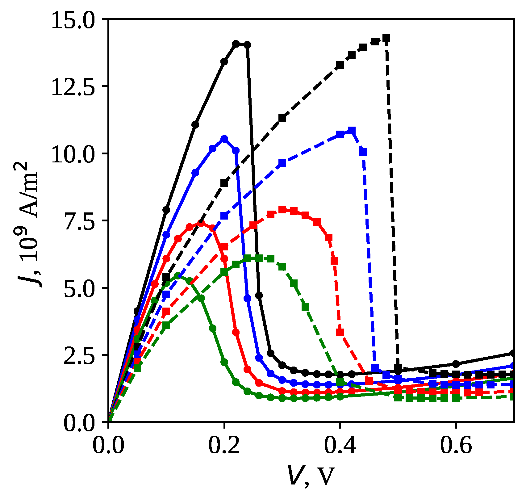
Figure 9 shows the current–voltage characteristics for different values of the thicknesses of the emitter and collector spacer, obtained by the calculations for the resonant tunneling Nanostructure #2. It can be seen from the results presented in
Figure 9 and
Table 2 and
Table 3 that the peak current and valley current values were generally preserved when the collector spacer thickness was varied, regardless of the chosen value of the emitter spacer thickness and the features of the RTD layer structure. Thus, the functional dependences of the peak current and valley current on the thickness of the emitter spacer and the thickness of the collector spacer were consistent with the experimental data presented in [
18,
19,
20,
21,
22]. The values of
and
increased monotonically with the increasing thickness of the collector spacer.
As shown in [
10], the maximum oscillator output power of the RTD can be estimated through the product
,
,
. From the data presented in
Table 2 and
Table 3, it can be seen that
weakly depends on the thickness of the collector spacer and decreased with the increasing thickness of the emitter spacer for all RTD structures considered. Moreover,
depends on both the thickness of the emitter spacer and the thickness of the collector spacer, as well as on the RTD structure.
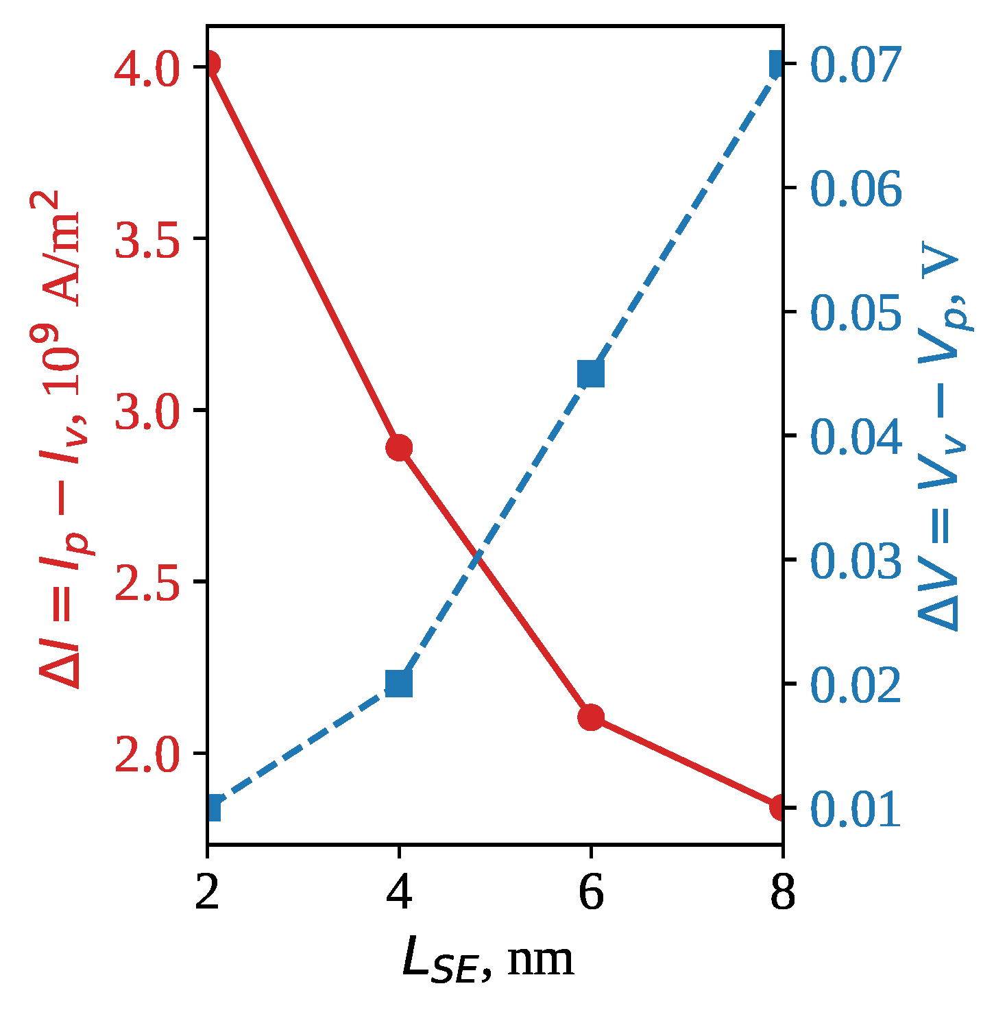
Figure 10 shows the dependences of
and
on
for Structure #1 at
nm. It can be seen that
decreased with the increasing thickness of the emitter spacer, while
increased. Thus, the product
can have a maximum value at a certain value of the emitter spacer (in the case considered in
Figure 10, the optimal value of the emitter spacer is 8 nm), which will depend on both the structure of the RTD and the chosen thickness of the collector spacer. This significantly complicates the analysis and search for general patterns of behavior of the value
for different RTD structures and requires the consideration of large intervals of spacer thickness variation in smaller increments.
One of the important parameters of the static current–voltage characteristic of resonant tunneling nanostructures is the peak-to-valley-current ratio (PVCR). In the range of thicknesses of the emitter spacer and collector spacer considered, for Structure #1, the PVCR is of the order of 4; for Structure #2, the PCVR is in the range of 6.9-8.2; for Structure #3, the PVCR is in the range of 7.2–8.7.
4. Conclusions
A method for calculating the static characteristics of resonant tunneling nanostructures based on the numerical solution of a non-stationary open Schrodinger–Poisson system of equations with a stepwise dependence of the applied voltage on time was developed. In the presented technique, the electroneutrality condition was performed with a high degree of accuracy, in contrast to the stationary numerical formulation, in which the associated divergences of the solution are observed at certain values of the emitter spacer thickness. The developed calculation method makes it possible to study the static characteristics of resonant tunneling nanostructures taking into account the features characteristic of the experiment, such as the presence of charge accumulation effects and the presence of heavily doped contact layers in the nanostructure. The use of exact discrete open boundary conditions, which require taking into account the entire prehistory, leads to a slowdown in the calculations over long periods. One possible way to improve the efficiency of the developed technique is to use perfectly matched layers (PMLs) [
33], instead of discrete open boundary conditions.
In the present study, we considered three different resonant tunneling nanostructures with a symmetric active region consisting of two barriers and a quantum well. The calculation method developed in this study was applied to the analysis of the effect of the emitter and collector spacers’ thickness on the most-important static characteristics of resonant tunneling nanostructures: peak current, valley current, and the corresponding values of the applied voltage. As a result of the numerical simulation, it was found that taking into account heavily doped contact layers and the effects of charge accumulation is extremely important. Taking into account these effects leads to a significant modification of the potential of the resonant tunneling nanostructure, which, in turn, is reflected in electronic transport. In this regard, the results of [
11,
12], obtained without taking into account these effects, undergo significant changes. The calculations in the work were carried out for three different resonant tunneling nanostructures, which suggests some generality of the results obtained. The numerical simulations showed that the peak current and valley current monotonically decrease with the increasing thickness of the emitter spacer. Thus, to obtain the maximum values of the peak current and peak-to-valley-current ratio, it is necessary to create the nanostructures with small values of the emitter spacer. The collector spacer weakly affects the values of the peak current and valley current, while having a strong influence on the values of the peak and valley voltage, so the collector spacer can have a strong influence on the output power of resonant tunneling nanostructures, as evidenced by the experimental results of [
6]. The observed peculiarities of the peak and valley current behavior from the thickness of the emitter spacer and collector spacer agreed well with the experimental data of [
18,
19,
20,
21,
22].
InGaAs-based structures with thin barriers (similar to Structure #3) give the highest peak current values and PVCR, while the operating voltages for this type of structures are quite large (∼1 V). The use of a quantum well material with a smaller band gap (as in Structure #2) makes it possible to significantly reduce the operating voltages (by about 3–4-times), but at the same time, the peak current value is also significantly reduced (by about 3-times).
It is important to note that the results obtained for the valley current values are significantly underestimated if the model based on the self-consistent solution of the Schrodinger and Poisson equations is used to calculate the properties of resonant tunneling nanostructures. For a more accurate description of the value of the valley current, impurity scattering and inelastic tunneling should be taken into account. This can be performed by modifying the current model following [
34]. It is worth noting that the peak current values obtained within similar coherent models usually agree quite well with the experiment [
20].
An important direction for further research is a detailed analysis of the effect of various prewells formed in the spacer region of the emitter, which, as experimentally shown [
35], can significantly modify the dependence of the peak current on the thickness of the spacer, leading to an increase in the peak current at a certain thickness of the prewell.
Furthermore, the results on transient processes in resonant tunneling nanostructures caused by rapid changes in the applied voltage were obtained. It was established that the transition times are weakly dependent on the thickness of the emitter spacer and have values of the order of 1 ps. The obtained transient times, along with sufficiently large values of the peak-to-valley ratio, indicate the prospects of using resonant tunneling nanostructures as high-speed switches. The most-promising nanosystems as ultrafast switches are structures with large values of the width of the resonant level, which can be most easily obtained by reducing the thickness of the barrier layers.


