Communication

Inhibited Channel Potential of 3D NAND Flash Memory String According to Transient Time

Department of Electronics Engineering, Korea National University of Transportation, Room No. 326, Smart ICT Building, 50 Daehak-ro, Chungju-si 27469, Chungbuk, Republic of Korea
*
Author to whom correspondence should be addressed.
These authors contributed equally to this work.
Appl. Sci. 2023, 13(5), 2909; https://doi.org/10.3390/app13052909
Submission received: 29 January 2023 / Revised: 21 February 2023 / Accepted: 21 February 2023 / Published: 24 February 2023
(This article belongs to the Section Materials Science and Engineering)

Abstract

:
The channel potential of natural local self-boosting (NLSB) effects in 16-layer 3D NAND flash memory was analyzed according to transient time. After a program pulse was applied to the selected word line (WL) of the inhibited string channel, the channel potential of the selected WL increased owing to NLSB. The channel potential of the selected WL, increased by NLSB, was analyzed as a function of the threshold voltage (Vth) of the adjacent cell and according to the change in time. The analysis confirmed that the channel potential value decreased gradually over time. However, it was confirmed that the rate at which the channel potential decreases was different depending on the Vth of the adjacent cell. The number of electrons in nitride is different for each Vth. These electrons affect the holes of the spacer and channel. The analysis also confirmed that the movement of electrons was caused by the difference in the hole concentration in the spacer and channel.

1. Introduction

Recently, efforts have been made to enhance the competitiveness of NAND flash memory in the semiconductor-based memory market by producing high-density and low-power memory technology [1]. However, the existing 2D structures have limitations. Because the 2D structure of NAND flash memory does not have a high degree of integration, and as the device size becomes smaller, problems such as cell-to-cell interference and limitations of lithography patterning occur [2,3]. As a result, it was difficult to store a large amount of data compared to the area. To solve this problem, 3D NAND flash memory can be used [4]. The structure of a 3D NAND flash memory uses an ultrathin-body structure in which the channel of the main cell is not connected to the body [5]. The floating state of the structure in which the channel is not connected to the body indicates that the body bias is unaffected by the channel of the main cell [6]. Because of this structural characteristic, the inhibited string channel is not directly connected to the body. Therefore, it can easily achieve a floating state [7,8]. As a result, when the program pulse is applied to the selected word line (WL) to proceed with the program, a phenomenon occurs in which the cell of the selected WL is localized in the inhibited string channel. This is called natural local self-boosting (NLSB). NLSB is a beneficial effect that can prevent program disturb [9,10]. However, the channel potential increased by NLSB is not maintained.
In this study, the channel potential for NLSB in a 16-layer 3D NAND flash memory was analyzed according to the transient time and threshold voltage (Vth) value change of adjacent cells. Through our analysis, it was confirmed that the reason why the channel potential is not maintained is related to the electrons of the nitride. The 3D-technology computer-aided design (TCAD) tool ATLAS (Silvaco) [11] was used to analyze the channel potential and electron concentration.

2. Structure of the Proposed 3D NAND Flash Memory

Figure 1a shows the 3D NAND flash memory structure used [12]. This structure is composed of tungsten (W)/oxide (O)/nitride (N)/oxide (O)/polycrystalline silicon (poly-Si) and there are 16 WLs (WL0–WL15). Figure 1a also shows that the channel is vertical and not connected to the body. Figure 1b shows the simulation pattern according to the Vth of the adjacent cell. The values of the E, P1, P2, and P3 patterns indicate the Vth of the WL cell (E = −1 V, P1 = 1 V, P2 = 2 V, P3 = 3 V). In the case of P1 in Figure 1b, pattern E was set to erase WL7–WL9, and the remaining adjacent WLs were set to P1. Case P2 and, P3 also erased WL7–WL9. The adjacent WL was set to P2 in Case P2, and the adjacent WL was set to P3 in Case P3.
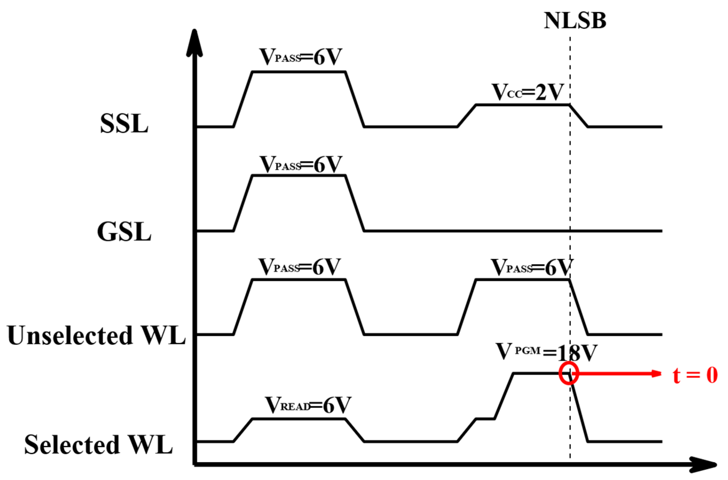
Table 1 lists the device parameters used in the TCAD simulation. Table 1 shows gate length (WL, string select line (SSL), ground select line (GSL)), gate spacing, gate dielectrics (O/N/O), channel hole diameter, Poly-Si channel thickness, VCC (bit line and SSL voltage), and doping (Arsenic/Boron). Figure 2 shows a time diagram of NLSB. In the diagram, the selected WL is WL8, and the unselected WL includes the rest of the WL, except WL8. NLSB is a phenomenon that occurs in the selected WL of the inhibited string. After the verification process is complete, the program process is started. When the program process starts, the channel becomes to floating state [13,14]. If a program is started while this state is maintained, pass voltage (VPASS) is applied to all the WLs, and the channel potential is increased by capacitive coupling [15]. At this time, because the cells on the selected WL are floating channels, they remain turned off and the channel potential increases according to VPASS. Subsequently, a program voltage (VPGM) is applied to the selected WL [16,17]. In the process of increasing the VPGM, electrons in the channel gather at the selected WL channel owing to the potential difference of the WL. Because of these electrons, the channel potential of the selected WL increases. This phenomenon of increasing the channel potential is called NLSB. NLSB has the effect of decreasing program disturbance. This is because unwanted programs are blocked owing to the selected WL channel potential increased in the inhibited string [18].

3. Results

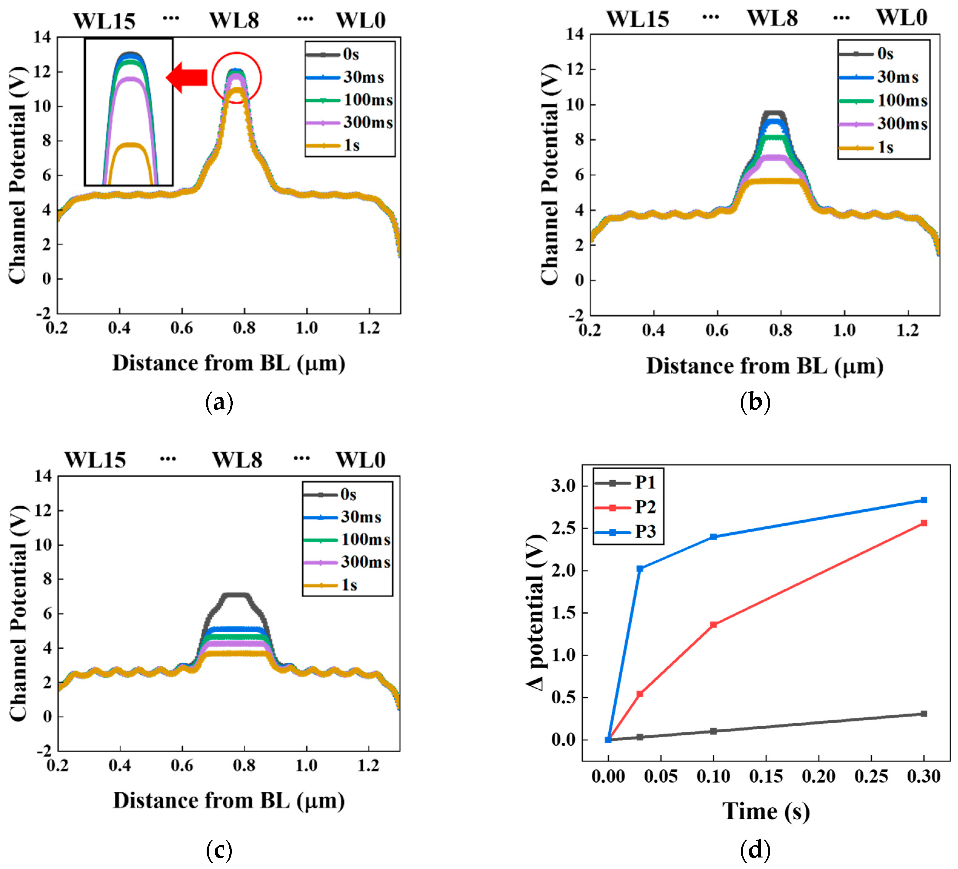
The advantage of NLSB is that the potential of the selected WL channel is higher than that of the unselected WL channel. However, Figure 3 confirms that the selected WL channel potential decreases over time. Figure 3 shows the channel potential changing over time after the NLSB phenomenon. Time(t) was measured at t = 0 s, 30 ms, 100 ms, 300 ms, and 1 s. Here, (t = 0 s) was set as the time at which the program pulse was applied, and the channel potential over time was observed. In the results in Figure 3a–c, the channel potential is the highest when the time is 0 s. Additionally, the channel potential gradually decreases over time. Eventually, the channel potential reaches its lowest value at 1 s. However, the rate at which the channel potential decreases in Figure 3a–c is different. The rate at which the channel potential decreased was the fastest in Figure 3c, whereas that in Figure 3a was the slowest. In Figure 3c, the selected WL channel potential became like unselected WL, but Figure 3a showed little change compared to Figure 3c, with a difference of approximately 1V. Figure 3d is a graph showing the Δ potential of Figure 3a–c. The graph in Figure 3d confirms that, the higher the Vth of the adjacent cell becomes, the faster the channel potential decreases.
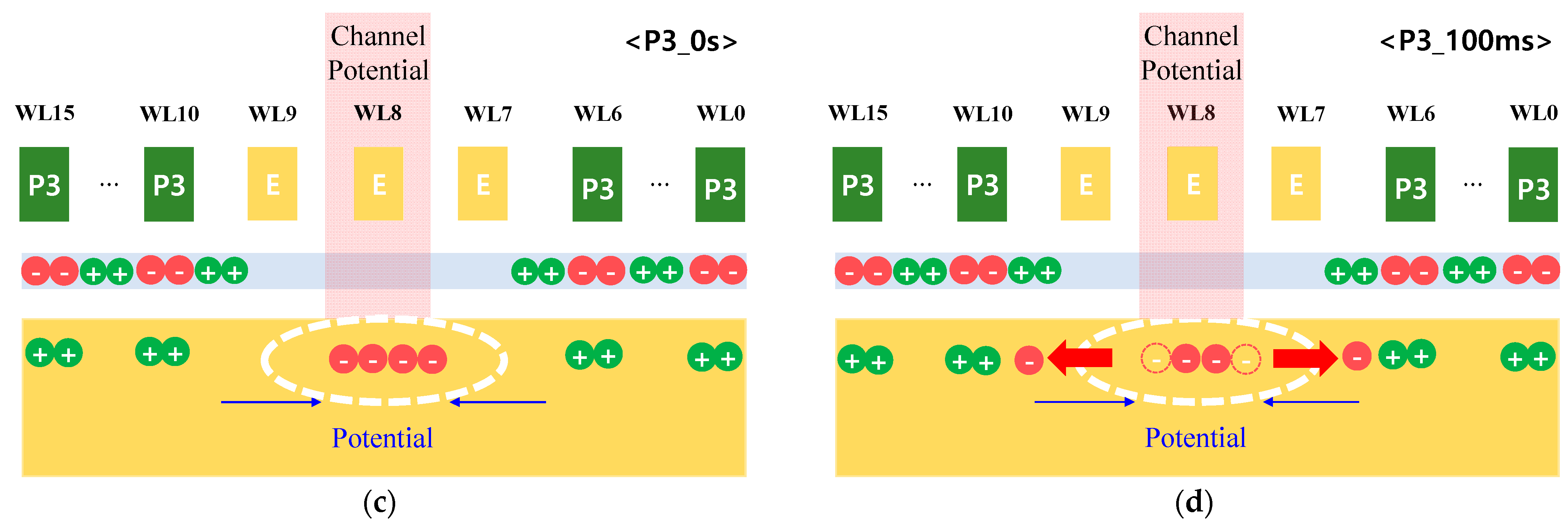
During NLSB, the electrons from the floated channels gather in the selected WL channel because of the potential difference. However, the gathered electrons spread out over time. Figure 4 shows the results 0 s and 100 ms after NLSB occurred at P1 and P3. This figure shows the differences in the electron concentration of the selected WL, observed at P1–P3 during the same time, result from the difference in the concentration of electrons trapped in the nitride and the holes in the spacer. The electrons trapped in nitride attract holes in the spacer and channel. These spacers and channel holes attract electrons in the selected WL channel. Owing to the influence of the holes in the channel and in the spacer, the electrons gathered under the selected WL channel spread to WL7 and WL9. There are more electrons in the nitride of P3 than in P1, resulting in P3 attracting more holes to channels and spacers than P1. Therefore, the electrons in the selected WL of P3 spread faster than those of P1. As a result, the channel potential of P3 decreases faster than that of P1 owing to the faster electron movement.
This can be proved in the electron concentration graph in Figure 5. Figure 5 is a graph of electron concentration according to transient time. Figure 5a shows no change in electron concentrations in the WL7 and WL9 channels, which increase over time for P1. However, Figure 5b shows that, for P3, the electrons spread to both sides over time, and the electron concentration in the WL7 and WL9 channels increase over time. Through this result, it can be confirmed that the explanation in Figure 4 is correct. Additionally, in Figure 5b, it can be seen that the electrons spread to WL7 and WL9, but not to the adjacent WL. This movements of electrons can be better confirmed when only one side of the WL is programmed. In Figure 5b, the Vth of WL7 and WL9 are E, and the other cells are P3. So, electrons spread to WL7 and WL9, which do not have electrons in nitride, and do not spread to the other cells that have electrons. However, in Figure 5c, the electron concentration is different between WL7 and WL9 channel. More electrons are spread in the WL7 channel than in WL9. Because electrons exist in the nitride of WL9, the electrons in the nitride of WL9 block the spreading electrons from selected WL. Because of this, the electrons in the selected WL channel move more to WL7 than to WL9 over time. As a result, the electrons of the nitride have an influence on the movement of electrons in the selected WL channels.

4. Conclusions

Owing to the structural characteristics of 3D NAND flash memory, the selected string channel floats under certain circumstances. As a result, the NLSB phenomenon occurs, and the channel potential of the selected WL increases because of this phenomenon. Regarding the structure, WL7, WL8, and WL9 were all erased from the 16-layer NAND flash memory, and all adjacent cells were applied separately as P1, P2, and P3. A comparative analysis of the channel potential according to time t = 0 s, 30 ms, 100 ms, 300 ms, and 1 s confirmed that the channel potential decreased over time when Vth of the adjacent cell was P1, P2, and P3. However, when the Vth of an adjacent cell changes, the rate of the decrease in the WL8 channel potential also changes. The higher the Vth of the adjacent cell, the faster the decrease in the channel potential of WL8. This phenomenon means that the decrease in the channel potential is different because of the influence on the Vth of the adjacent cell. In P3, which has the fastest rate, the selected WL channel potential decreases the fastest and becomes like unselected WL. The reason for this phenomenon is the fact that the more electrons that become trapped in the nitride, the more holes there will be in the spacer and channel. Owing to the influence of these holes, the electrons in the selected WL channel move easily to the adjacent WL channel. These results suggest that the rate of the channel potential decrease is influenced by the electrons in the nitride. The more electrons present in the nitride, the faster the rate of decrease in the channel potential. This analysis shows why a lower Vth is more resistant to program disturbance. Program disturbance is a problem with the reliability of the device. However, lowering Vth to reduce program disturbance can cause other problems. Therefore, it is necessary to find other ways than to lower Vth. This study will assist the scientific community to find other ways.

Author Contributions

Data curation, software, and writing (original draft preparation), T.C.; project administration, H.K.; project administration, funding acquisition, supervision, and visualization, M.K. All authors have read and agreed to the published version of the manuscript.

Funding

This research was supported by the National R&D Program through the National Research Foundation of Korea (NRF) funded by Ministry of Science and ICT (2021M3F3A2A03017693), and in part by the Basic Science Research Program through the National Research Foundation of Korea (NRF) funded by the Ministry of Education (2018R1A6A1A03023788).

Institutional Review Board Statement

Not applicable.

Informed Consent Statement

Not applicable.

Data Availability Statement

Data sharing not applicable.

Conflicts of Interest

The authors declare no conflict of interest.

References

  1. Kim, Y.; Yun, J.G.; Park, S.H.; Kim, W.; Seo, J.Y.; Kang, M.; Ryoo, K.C.; Oh, J.H.; Lee, J.H.; Shin, H.; et al. Threedimensional NAND flash architecture design based on single-crystalline stacked array. IEEE Trans. Electron Devices 2011, 59, 35–45. [Google Scholar] [CrossRef]
  2. Jeong, W.; Im, J.W.; Kim, D.H.; Nam, S.W.; Shim, D.K.; Choi, M.H.; Yoon, H.J.; Kim, D.H.; Kim, Y.S.; Park, H.W.; et al. A 128 Gb 3b/cell V-NAND Flash Memory With 1 Gb/s I/O Rate. IEEE J. Solid-State Circuits 2016, 51, 204–212. [Google Scholar]
  3. Jang, J.; Kim, H.S.; Cho, W.; Cho, H.; Kim, J.; Shim, S.I.; Jeong, J.H.; Son, B.K.; Kim, D.W.; Shim, J.J.; et al. Vertical cell array using TCAT(Terabit Cell Array Transistor) technology for ultra-high density NAND flash memory. In Proceedings of the 2009 Symposium on VLSI Technology, Kyoto, Japan, 15–17 June 2009; IEEE: Piscataway, NJ, USA, 2009; pp. 192–193. [Google Scholar]
  4. Kim, Y.; Seo, J.Y.; Lee, S.-H.; Park, B.-G. A new programming method to alleviate the program speed variation in three-dimensional stacked array NAND flash memory. J. Semicond. Technol. Sci. 2014, 14, 566–571. [Google Scholar] [CrossRef] [Green Version]
  5. Jeong, M.-K.; Joe, S.-M.; Jo, B.-S.; Kang, H.-J.; Bae, J.-H.; Han, K.-R.; Choi, E.; Cho, G.; Park, S.-K.; Park, B.-G.; et al. Characterization of traps in 3-D stacked NAND flash memory devices with tubetype poly-Si channel structure. In Proceedings of the 2012 International Electron Devices Meeting, San Francisco, CA, USA, 10–13 December 2012; pp. 9.3.1–9.3.4. [Google Scholar]
  6. Park, Y.; Lee, J.; Cho, S.S.; Jin, G.; Jung, E. Scaling and reliability of NAND flash devices. In Proceedings of the 2014 IEEE International Reliability Physics Symposium, Waikoloa, HI, USA, 1–5 June 2014; pp. 2E.1.1–2E.1.4. [Google Scholar] [CrossRef]
  7. Park, M.; Kim, K.; Park, J.-H.; Choi, J.-H. Direct field effect of neighboring cell transistor on cell-to-cell interference of NAND flash cell arrays. IEEE Electron Device Lett. 2008, 30, 174–177. [Google Scholar] [CrossRef]
  8. Park, K.T.; Nam, S.; Kim, D.; Kwak, P.; Lee, D.; Choi, Y.H.; Choi, M.H.; Kwak, D.H.; Kim, D.H.; Kim, M.S.; et al. Three-dimensional 128 Gb MLC vertical NAND flash memory with 24-WL stacked layers and 50 MB/s high-speed programming. IEEE J. Solid-State Circuits 2014, 50, 204–213. [Google Scholar] [CrossRef]
  9. Ham, I.; Jeong, Y.; Baik, S.J.; Kang, M. Ferroelectric polarization aided low voltage operation of 3D NAND flash memories. Electronics 2020, 10, 38. [Google Scholar] [CrossRef]
  10. Kim, Y.; Kang, M. Down-coupling phenomenon of floating channel in 3D NAND flash memory. IEEE Electron Device Lett. 2016, 37, 1566–1569. [Google Scholar] [CrossRef]
  11. Atlas User’s Manual, Silvaco Version. 5.19.20. Available online: http://www.silvaco.com/products/tcad/device_simulation/atlas/atlas.html (accessed on 3 February 2020).
  12. Kim, H.; Kang, M. Analysis of DCP and NLSB Recovery Time in 3D NAND Flash Memory. Knut Dcollection. February 2023. Available online: http://www.dcollection.net/handler/chains/200000667859 (accessed on 3 February 2023).
  13. Jung, S.G.; Lee, K.W.; Kim, K.S.; Shin, S.W.; Lee, S.S.; Om, J.C.; Bae, G.H.; Lee, J.H. Modeling of VTH shift in NAND Flash memory cell device considering crosstalk and short channel effect. IEEE Trans. Electron Devices 2008, 55, 1020–1026. [Google Scholar] [CrossRef]
  14. Choi, B.Y.; Sung, S.K.; Park, S.J.; Kim, T.H.; Kim, M.; Lee, S.H.; Kim, M.J.; Kwon, S.H.; Jang, D.H.; Hyun, K.S.; et al. New source/drain hot carrier injection disturbance of NAND Flash devices. J. Korean Phys. Soc. 2010, 56, 142–146. [Google Scholar] [CrossRef]
  15. Lee, J.-D.; Lee, C.-K.; Lee, M.-W.; Kim, H.-S.; Park, K.-C.; Lee, W.-S. A new programming disturbance phenomenon in NAND Flash memory by source/drain hot-electron generated by GIDL current. In Proceedings of the 2006 21st IEEE Non-Volatile Semiconductor Memory Workshop, Monterey, CA, USA, 12–16 February 2006; pp. 31–33. [Google Scholar]
  16. Larcher, L.; Padovani, A.; Pavan, P.; Fantini, P.; Calderoni, A.; Mauri, A.; Benvenuti, A. Modeling NAND Flash memories for IC design. IEEE Electron. Device Lett. 2008, 29, 1152–1154. [Google Scholar] [CrossRef]
  17. Lee, D.; Chang, I.J.; Yoon, S.-Y.; Jang, J.; Jang, D.-S.; Hahn, W.-G.; Park, J.-Y.; Kim, D.-G.; Yoon, C.; Lim, B.-S.; et al. A 64Gb 533Mb/s DDR interface MLC NAND Flash in sub-20nm technology. In Proceedings of the 2012 IEEE International Solid-State Circuits Conference, San Francisco, CA, USA, 19–23 February 2012; pp. 430–432. [Google Scholar]
  18. Kang, M.; Kim, Y. Natural local self-boosting effect in 3D NAND flash memory. IEEE Electron. Device Lett. 2017, 38, 1236–1239. [Google Scholar] [CrossRef]
Figure 1. (a) Structure of 3D NAND flash memory and (b) simulation pattern according to the Vth of the adjacent cell.
Applsci 13 02909 g001
Figure 2. Timing diagram of NLSB (VCC = 2 V, VPASS = VREAD (read voltage) = 6 V, VPGM = 18 V).
Applsci 13 02909 g002
Figure 3. NLSB effect analysis according to transient time (a) Vth = P1, (b) Vth = P2, (c) Vth = P3 and (d) is the Δ potential of selected WL at P1, P2, and P3.
Applsci 13 02909 g003
Figure 4. Schematic diagram of P1 at (a) 0 s and (b) 100 ms, and P3 at (c) 0 s and (d) 100 ms after NLSB occurred.
Applsci 13 02909 g004aApplsci 13 02909 g004b
Figure 5. Electron concentration profiles for various transient time of (a) P1 and (b) P3, whereas (c) is graph of electron concentration when WL9 is programmed as P3.
Applsci 13 02909 g005
Table 1. Device parameters used in the simulation.
QuantityValue
Gate length (WL)40 nm
Gate length (SSL, GSL)150 nm
Gate spacing30 nm
Gate dielectrics (O/N/O)4/8/8 nm
Channel hole diameter 80 nm
Poly-Si channel thickness 10 nm
Selected WLWL8
VCC2 V
Doping (Arsenic/Boron)1 × 1020/cm3/1 × 1018/cm3
Disclaimer/Publisher’s Note: The statements, opinions and data contained in all publications are solely those of the individual author(s) and contributor(s) and not of MDPI and/or the editor(s). MDPI and/or the editor(s) disclaim responsibility for any injury to people or property resulting from any ideas, methods, instructions or products referred to in the content.