Review

Overview on Different Types of Solar Cells: An Update

1
Faculty of Health and Life Sciences, INTI International University, Putra Nilai 71800, Malaysia
2
Politeknik Medica Farma Husada Mataram, Mataram 83116, Indonesia
3
Department of Energy Science, Sungkyunkwan University (SKKU), Suwon 440-746, Republic of Korea
4
Energy and Materials Research Lab, Department of Physics, College of Natural and Mathematical Sciences, University of Dodoma, Dodoma P.O. Box 338, Tanzania
5
Department of Physics, Sefako Makgatho Health Sciences University, P.O. Box 94, Medunsa 0204, South Africa
6
Third World Center for Science and Technology, H.E.J. Research Institute of Chemistry, International Center for Chemical and Biological Sciences, University of Karachi, Karachi 75270, Pakistan
*
Author to whom correspondence should be addressed.
Appl. Sci. 2023, 13(4), 2051; https://doi.org/10.3390/app13042051
Submission received: 17 December 2022 / Revised: 9 January 2023 / Accepted: 17 January 2023 / Published: 4 February 2023
(This article belongs to the Special Issue Thin Films Technology and Application)

Abstract

:
Solar energy is free from noise and environmental pollution. It could be used to replace non-renewable sources such as fossil fuels, which are in limited supply and have negative environmental impacts. The first generation of solar cells was made from crystalline silicon. They were relatively efficient, however very expensive because they require a lot of energy to purify the silicon. Nowadays, the production of solar cells has been improved since the first generation (thin-film solar cells, dye-sensitized solar cells, perovskite solar cells, and organic solar cells). In this work, the development of solar cells was discussed. The advantages, limitations, challenges, and future trends of these solar cells were also reported. Lastly, this article emphasized the various practices to promote solar energy and highlighted the power conversion efficiency of the fabricated devices.

1. Introduction

The process of the conversion of energy from the most abundant source, the sun, into electricity is termed as the photovoltaic effect [1]. Semiconductor materials are the basic requirement for the process of the conversion of photons into electrons [2]. These materials can be divided into organic and inorganic [3] substances.
Photovoltaic solar-cell technologies can be divided into three distinct generations [4]. The first generation was crystalline silicon. This technology currently dominates the global solar-cell market due to it has good performance and stability. The second generation is based on thin films of amorphous silicon and inorganic semiconductor elements such as copper indium gallium selenide (CIGS), cadmium telluride (CdTe), and copper indium selenide (CuInSe2). Moreover, the third generation is based on organic semiconductors. Organic solar cells can either be based on dye-sensitized solar cells [5], multiple junctions based on group IV and group III–V elements, and hybrid solar cells that contain inorganic quantum dots or nanomaterials with organic materials [6]. The potential of organic solar cells for practical applications [7] is demonstrated by recent enhancements in the power-conversion efficiency (PCE).
Organic–inorganic hybrid perovskites (OIHPs) are a group of materials which show magnificent potential for high performance and low production costs in photovoltaic technology [8]. Any material which has an identical crystal structure with calcium titanium oxide (CaTiO3) is recognized as a “perovskite” structure, as named by the Russian Mineralogist Lev Alek-sevich von Perrovski (1839). These perovskites have a stoichiometry of ABX3 three-dimensional structure, where the “A” and “B”-sites are occupied by larger and smaller cations, respectively, and the anion resides at the “X”-site. The 3D crystal structure of ABX3 consists of corner-shared BX6 octahedrals and “A” cations occupy the cavity between them [9,10]. Materials with perovskite structures are quite abundant in nature and can be found in an enormous number of compounds that show a wide range of physical properties, applications, and importance.
Perovskite solar cells can have a conventional (regular) or an inverted PSC structure, depending on the architecture. TiO2 and n-type semiconductors are used in the normal configuration, whereas p-type poly (3,4-ethylene dioxythiophene)-poly(styrene sulfonate) (PEDOT: PSS) are used in the inverted configuration. Typical mesoscopic perovskite solar cell structures consist of a glass surface with a transparent conducting oxide (TCO), such as in FTO (F:SnO2), in which an anode is deposited on the glass substrate, a dense (compact) layer of TiO2 is a hole-blocking layer, and a mesoporous layer of TiO2 serves as an electron-transporting layer (ETL). Moreover, a layer of the perovskite material is used for light absorption, followed by a hole-transporting layer, followed by metal contacts to complete the device’s structure. This type of solar cell has an organic material with a perovskite structure in its absorbing layer, most typically a lead–metal hybrid (Methylammonium lead iodide perovskite, MAPbI3). Methylammonium lead iodide is an ambipolar semiconductor that may transmit both electrons and holes to the collecting electrodes. Because of this, perovskite solar cells can operate without a hole or electron conductor. The Spiro-OMeTAD polymer composition is the HTL material most frequently utilized in perovskite solar cells.
Perovskite solar cells’ superior absorption capabilities and low exciton binding energy are two of their most notable features. Light absorption is the initial physical process in solar systems. When a photon activates an active material with an energy higher than its bandgap, an exciton (electron-hole pairs) is produced. Excitons must reach the contacts after being photogenerated in the perovskite to be retrieved. The charge-transport capabilities of the perovskite play a role in this process. Compared with conventional solar cells, perovskite serves as an absorber in thin-film solar cells to offer effective transport of excitons. The remarkable PCE of these perovskite solar cells is produced by the material’s outstanding charge-transport properties. They possess long charge-carrier diffusion lengths surpassing 5 m and the associated lifetimes of 1 s in both single-crystal and polycrystalline films. These diffusion lengths guarantee that the produced charge can be recovered even from thicker films that absorb the input light completely. However, the interfacial contacts with the charge extraction layer also have a role in the device’s ultimate quality. After absorption and charge transmission, the photovoltaic process requires the extraction of the photogenerated charge. As a result, the optimal extraction interface should provide the least possible voltage, current, and FF loss. An optimal selective contact should not absorb light to prevent the reduction of light intensity in the perovskite. Similarly, there should not be any energetic losses during the absorber injection (no interfacial recombination). These contact materials need to be selective to enable one kind of carrier to be injected, but they also need to lower series resistance.
One of two major processes can result in charge separation in perovskite. One involves injecting photogenerated electrons into an n-type semiconductor such as TiO2, while the other involves injecting holes into a p-type material that transports holes, such as spiro-OMeTAD. To stop holes from reaching the TCO substrate (anode) and short-circuiting the cell, a hole-blocking layer is utilized between the TCO-conducting substrate and the mesoscopic scaffold and/or perovskite layer. On the other hand, using a mesoporous TiO2 layer greatly lessens the hysteresis behavior of PSC even if a hybrid organic–inorganic perovskite absorber can transfer photogenerated electrons to the conductive substrate itself.
Dye-sensitized solar cells (DSSC) were first discovered by professor Michael Gratzel in 1991. The DSSC consists of a working electrode [11], a counter electrode, and an electrolyte. Dyes (natural organic materials and synthetic materials) are attached to the TiO2 films, serve as the working electrodes. The DSSC consisting of ruthenium (II) polypyridyl complex (N3 dye) [12] showed a power-conversion efficiency of about 10%. A platinum conductive glass served as the counter electrode [11]. The working principle of DSSC converts sunlight into electricity through the creation of exciton. The semiconductor material is placed on a conductive transparent plate to form a thin layer. A dye monolayer layer is placed on the surface of the semiconductor. Photoexcitation experienced by the dye produces electrons excited from the valence band to the conduction band of the dye, which then enter the conduction band of the metal oxide. This electron injection is performed through the connection between titanium and the carboxyl group in the dye. This process produces a positively charged dye and a negatively charged TiO2 particle. The electrons then exit through the external circuit to the opposite electrode. This flow of electrons is used as electrical energy. The electron vacancies in the valence band of the dye are replaced by electrons from the electrolyte. The electrolyte used in DSSC is usually an organic solvent containing a redox system such as an iodide–triiodide pair. The regeneration of the sensitizer by iodide occurs by donating electrons in the valence band of the oxidized dye. The iodide is regenerated by reducing the triiodide at the opposite electrode by utilizing electrons from the external circuit. This process takes place continuously as a cycle so that a continuous current is produced.
Metal chalcogenide films are considered as important materials for solar-cell applications [13]. Several types of films (metal sulfide, metal selenide, and metal telluride) have been prepared using a vacuum method or non-vacuum deposition technique [14]. These films could be cheaper to produce, show good quality materials, and have the most potential for the future.
In this work, the advantages and limitations of each type of solar cell (thin-film solar cells, dye-sensitized solar cells, and organic solar cells) were highlighted. Photovoltaic parameters were investigated based on the selected literature review.

2. Organic Solar Cells

2.1. Advantages of Organic Solar Cells over Inorganic Solar Cells

The advantages of organic solar cells (OSC) over inorganic solar cells are threefold [15,16]. Firstly, in terms of the materials, limited silicon wafer technology leads to heavy, rigid, fragile, and bulky materials that are only available in a couple of colors. Conversely, the materials for OSC are light-weight, thin, flexible, and color-tunable, and can be customized to any design. Secondly, the fabrication process of inorganic solar cells is expensive, complicated, energy-intensive, must be conducted at high temperatures, and has limitations in the possible sizes of fabrications. On the other hand, OSC technology is cheap, simple, non-energy consuming, can be fabricated at ambient temperature, has no limitations in the size of fabrication, and has high speed production besides various possibilities of printing and coating fabrication techniques (such as inkjet, screen, and spray). Finally, the applications of inorganic solar cell are limited only to rooftops and open fields compared with the unlimited possibilities of OSC applications such as windows, screens, smart glasses, automotives, and the charging of mobile devices and laptops [17,18,19].

2.2. Challenges for Organic Solar Cell Technology

Silicon is the most widely used material for the commercial photovoltaic market due to its high-power conversion efficiency [20,21,22]. Inorganic solar cells are associated with certain challenges such their its high-cost and complicated and energy-intensive fabrication protocols. Organic solar cells are gaining attention due to their simple fabrication protocols. OSC technology has not yet gained much attention commercially because of its low power-conversion efficiency (PCE) and limited lifetime [23,24]. The heterojunction generated by contact of donor and acceptor material is the basis of OSC. There are a number of challenges in OSC technology such as limited absorption efficiency of donor materials, hindered exciton diffusion, charge dissociation, and transport of charges. Different approaches to overcome these challenges could be improved in exciton diffusion length, crystal structure, and the collection of photogenerated carriers. These improvements can be realized by the application of polymer-based nanocomposites, plasmonics, and tandem architectures. Moreover, hybrid nanocomposites (composed of both organic and inorganic materials) can be a synergistic combination to take advantage of the unique properties of both components [25,26,27]. The operation of hybrid solar cells has more similarities with OSC. Hybrid solar cells are composed of n-type inorganic material along with p-type semiconductor polymer and are capable of achieving high PCE.

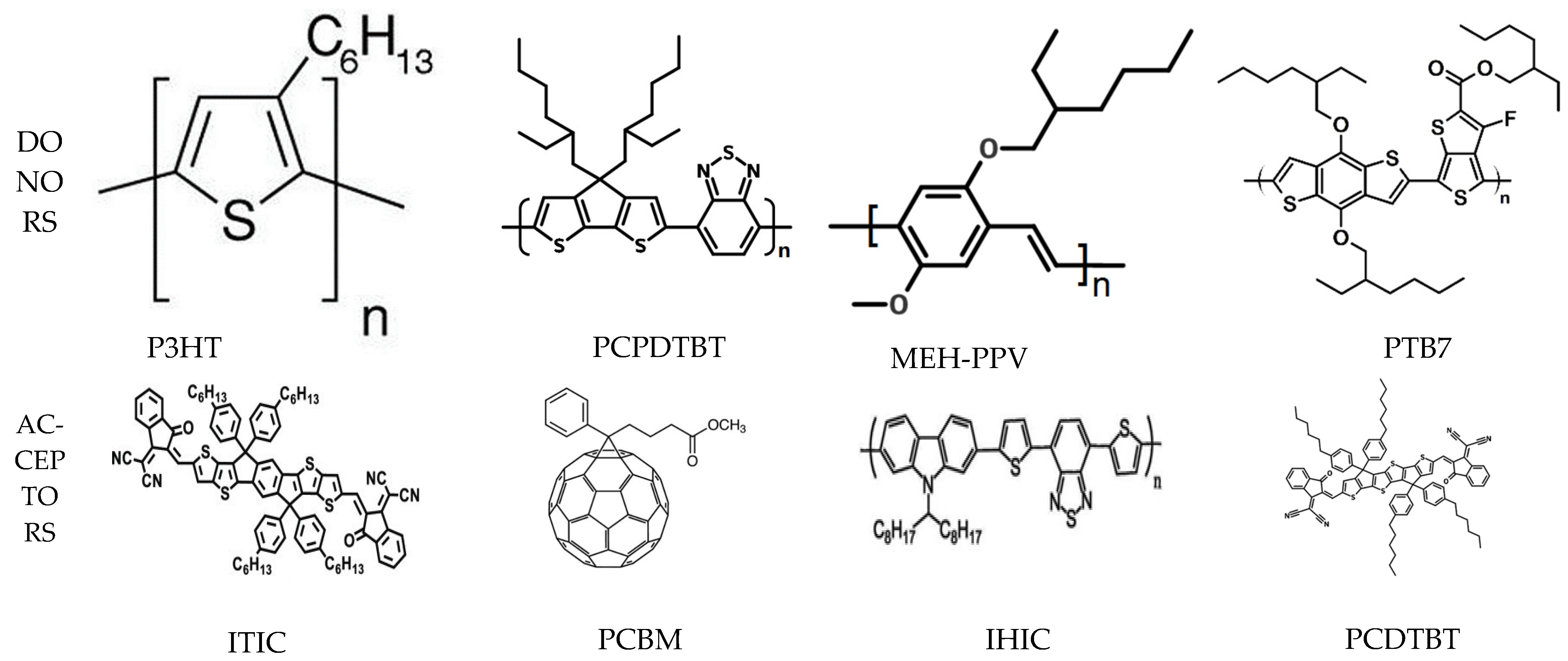
2.3. Materials for Organic Solar Cells

Organic materials for OSC can be derivative of small molecules or semiconducting polymers [28]. Organic semiconductors have conjugated organic moieties such as dendrimers, pigments, dyes, polymers, and small molecules, which can be a good choice for OSC. Any OSC requires two types of materials: an electron pair donor and an electron pair acceptor. Conjugated polymers are employed as donor materials. Initially, poly(1,4-phenylenevinylene) (PPV) and its derivatives gained considerable attention due to their appropriate optoelectronic properties [29,30]. Later, polythiophene and its derivative, especially poly(3-hexylthiophene), P3HT, began to be used widely (as a donor material) owing to its stability, high carrier mobility, and solubility [31,32,33]. The structures of some important donor materials for OSC technology are listed in Figure 1. Although fullerene and its derivatives dominated OSC technology in the initial phase [34,35,36,37,38], small molecules such as 3,9-bis(2-methylene-(3-(1,1-dicyanomethylene)-indanone)-5,5,11,11-tetrakis(4hexylphenyl)-dithieno [2,3-d:2′,3′-d′]-s-indaceno [1,2-b:5,6-b′]dithiophene (ITIC), IHIC, and PCDTBT (termed as non-fullerene acceptors, NFA) have attracted considerable attention recently due to their superior properties [39,40,41,42]. Moreover, donor–acceptor conjugated polymers such as poly [2,6-(4,4-bis-(2-ethylhexyl)-4H-cyclopenta [2,1-b;3,4-b′]dithiophene)-alt-4,7(2,1,3-benzothiadiazole)], PCPDTBT [43], and poly [2,7-(9,9-dioctylcarbazole)-alt-4,7-bis(thiophen-2-yl)benzo-2,1,3-thiadiazole], PCzDTBT [44] have been employed. The structures of some important fullerene and non-fullerene acceptor materials are depicted in Figure 1.
The engineering of the input donor and acceptor materials can help in improving the optoelectronic properties of these materials, which, in turn, improve the performance of OSC. One of the major limitations of the donor materials for OSC is their limited capacity of absorbing the whole wavelength range of the solar spectrum. The absorption efficiency can be improved by increasing the HOMO level, decreasing the LUMO level, or by compressing the band gap between HOMO–LUMO levels [45,46]. Polymers have higher molar mass and possess longer conjugation lengths, and hence the energy band gap is lower [47,48,49]. Voltametric p-type doping can also help in improving the optoelectronic properties through broadening of the absorption spectrum [50,51,52,53]. Regioregularity of polymers facilitates the mobility of excitons and thus improve the performance of OSC [54,55,56]. Physiochemical properties of OSC materials can be easily tuned by changing their chemistry, which is a unique advantage compared with conventional inorganic solar cells. For instance, the introduction of flexible side-chains such as alkyl or alkoxy leads to an improvement of solubility while the introduction of electron-donating or -withdrawing substituents can help in the alignment of electronic energy levels. The improvement of the optoelectronic properties of polymers by chemical modifications is shown for several polymers such as poly(p-phenylene vinylene) [57] and P3HT [58,59,60]. Electron-withdrawing groups such as Fluorine on the polymer chain improve the charge transference by tuning of the LUMO level [61], while electron-donating substituents on the polymer chain enhance charge-carrier mobility by minimizing the structural defects due to an increase in the HOMO energy level [62,63,64].
Moreover, large donor–acceptor interfaces as provided by nanostructures render effective exciton dissociation and efficient charge transport [65,66,67,68,69,70,71,72]. Conjugated polymer-based metallic nanoparticles can be prepared by several methods [73,74,75]. Different metals can have peculiar and dissimilar effects on the optoelectronic properties of the nanocomposites and their performance in the context of solar cells [76,77,78,79,80]. The incorporation of silver (Ag) and gold (Au) nano particles in polymer bulk heterojunction solar cells enhances their performance owing to the improved absorption of sunlight. In the context of OSC, conjugated polymer nanowires are mostly used due to their ability to create percolation pathways for both electrons and holes, leading to higher device efficiency [81,82,83,84]. The applications of polymer nanowires have several advantages such as (a) better control over morphology, (b) appropriate matching of the exciton diffusion lengths to the widths and lengths of polymer nanowires, (c) large interfacial area between donor and acceptor, (d) existence of electrically bi-continuous morphology, (e) achievement of high absorption coefficient and high carrier mobilities, (f) possibility of manufacturing devices with high surface areas, and (g) the avoidance of blend phase-separation difficulties [85,86]. Thermal annealing of the P3HT/PCBM mixture at 120 °C for 60 min renders P3HT nanowires with improved crystallinity of P3HT and enhances the demixing between P3HT and PCBM [87].

2.4. Fabrication of Organic Solar Cells

Organic photovoltaics fabricated as one active layer are termed as single-layer OPVs, while multiple active layers based OPV are termed as multiple layers or hetero-junctions [88]. Single-layer OPVs suffer from low PCE. The introduction of multiple layers or heterojunctions in OPVs results in an improvement in the OSC. The process of a heterojunction OPV consists of four distinct steps, namely, (i) the generation of an electron-hole pair (exciton) by absorption of the photon, (ii) diffusion of the exciton to the interface, (iii) the generation of free carriers by the dissociation of excitons, and (iv) carrier transport and collection at the electrode. The first generation of OSC was comprised of a single layer possessing very low PCE due to inefficient dissociation exciton (Figure 2A).
Later developments in OSC technology led to heterojunction cells that could be subdivided into bilayer heterojunctions, bulk heterojunctions, and tandem heterojunctions. In bilayer or planer heterojunctions, layers of donor and acceptor materials are sandwiched between two electrodes (Figure 2B). Planer heterojunctions also suffer from low PCE due to their short diffusion length and the low mobility of the generated excitons. In order to improve the PCE, it is required to match the diffusion length to the dimensions of the bilayer heterojunction, ultimately resulting in ultrathin films with low optical absorption.
On the other hand, dispersed or bulk heterojunctions are composed of blends of donor and acceptor materials (Figure 2C). Bulk heterojunctions facilitate the diffusion of excitons to the interface and achieve high PCE compared with planar heterojunctions. The most widely used combination of donor and acceptor materials for bulk heterojunctions is P3HT: PCBM [89,90]. The PCE has improved by up to 18% for bulk heterojunctions [91,92,93]. The absorption of light in single-layer, bilayer, and bulk heterojunction is limited to a small window of the visible light spectrum: either the short- or long-wavelength region. Tandem heterojunction provides an opportunity to exploit a wide wavelength region based on two sub-cells with complementary absorption spectra [94,95]. The sub-cells are separated by an interlayer that is responsible for the alignment of the quasi-Fermi level of both cells (Figure 2D). Owing to the elaborated advantages, tandem solar cells are gaining more attention recently. Tandem inorganic solar cells are restricted by the high cost for the required crystal growth and lattice matching. However, tandem OSC is gaining increasing interest and application owing to the simple and economical manufacturing. For bulk heterojunctions, the input materials should possess matched absorption spectra, appropriate energy level alignment, nanoscale phase separation, and high charge mobility [96].

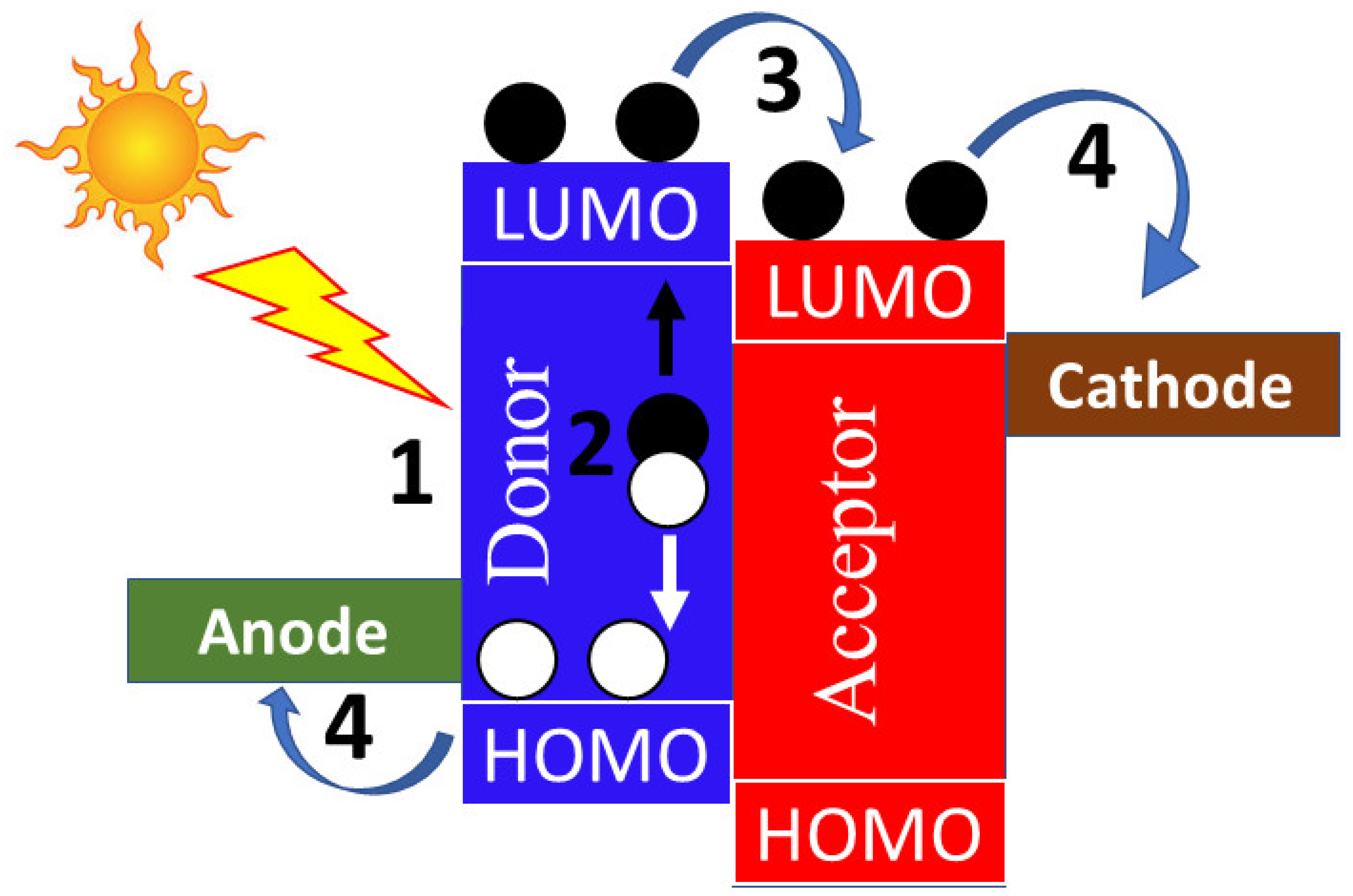
2.5. Operation of Organic Solar Cells

The operation of OSC is completely different from that of conventional silicon-based inorganic solar cells in terms of the material properties and architecture [97]. Free charge carriers are not immediately created by absorption of light in OSC, unlike traditional inorganic solar cells. An electrically neutral electron-hole pair is formed (as an exciton). It is a tightly bound electron-hole pair with a life span in the order of nano-seconds. The design and geometry of OPV devices are largely impacted by the excitonic character of the organic semiconductor material. The understanding of the basic operation of OPV is imperative for coping with the limitations and challenges of the materials and fabrication. The dissociation of the exciton is necessary for the generation of the photovoltaic effect. Exciton binding energy is in the range of 0.3–1.0 eV. Obviously, more energy than the binding energy is required to dissociate excitons and free the carrier. This is a relatively high energy requirement compared to its inorganic counterpart. The light is absorbed by the acceptor, resulting in creation of excitons. If the thermal energy generated is less than the exciton binding energy, electron and hole will undergo recombination. However, if the thermal energy is more than the exciton binding energy, free charges will be created that result in the separation of the electron and hole. Consequently, photogenerated carriers accumulate on the electrodes, electrons at the cathode, and holes at the anode. The working principle of OSC is demonstrated in Figure 3. The absorption of sunlight results in the generation of an electron-hole pair (exciton). High energy absorption leads to valence electrons of the donor jumping from their highest occupied molecylar orbital (HOMO) to the least unoccupied molecular orbital (LUMO) level, leaving behind holes at the HOMO level (separation of excitons into electrons and holes). Electrons then jump from the LUMO of the donor to the LUMO of the acceptor, which is at a lower energy level. Finally, the electrons from the LUMO of the acceptor are transported and collected at the cathode while holes at the HOMO of the donor are transported to anode, which completes the circuit. In this context, the alignment of the energy levels of the donor and acceptor materials, the absorption profiles, mobility of charges, and miscibility of the materials are critical factors [98].

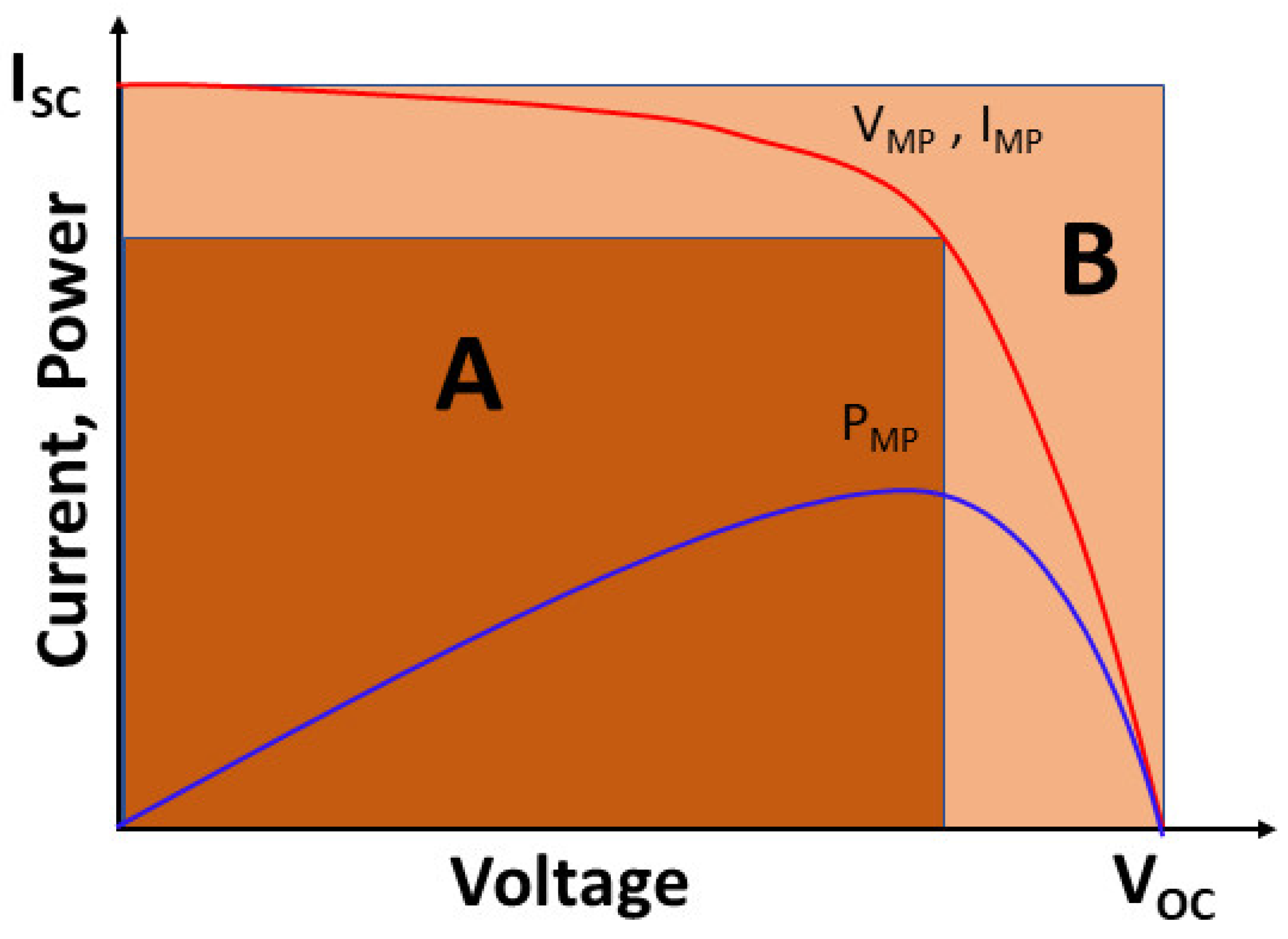
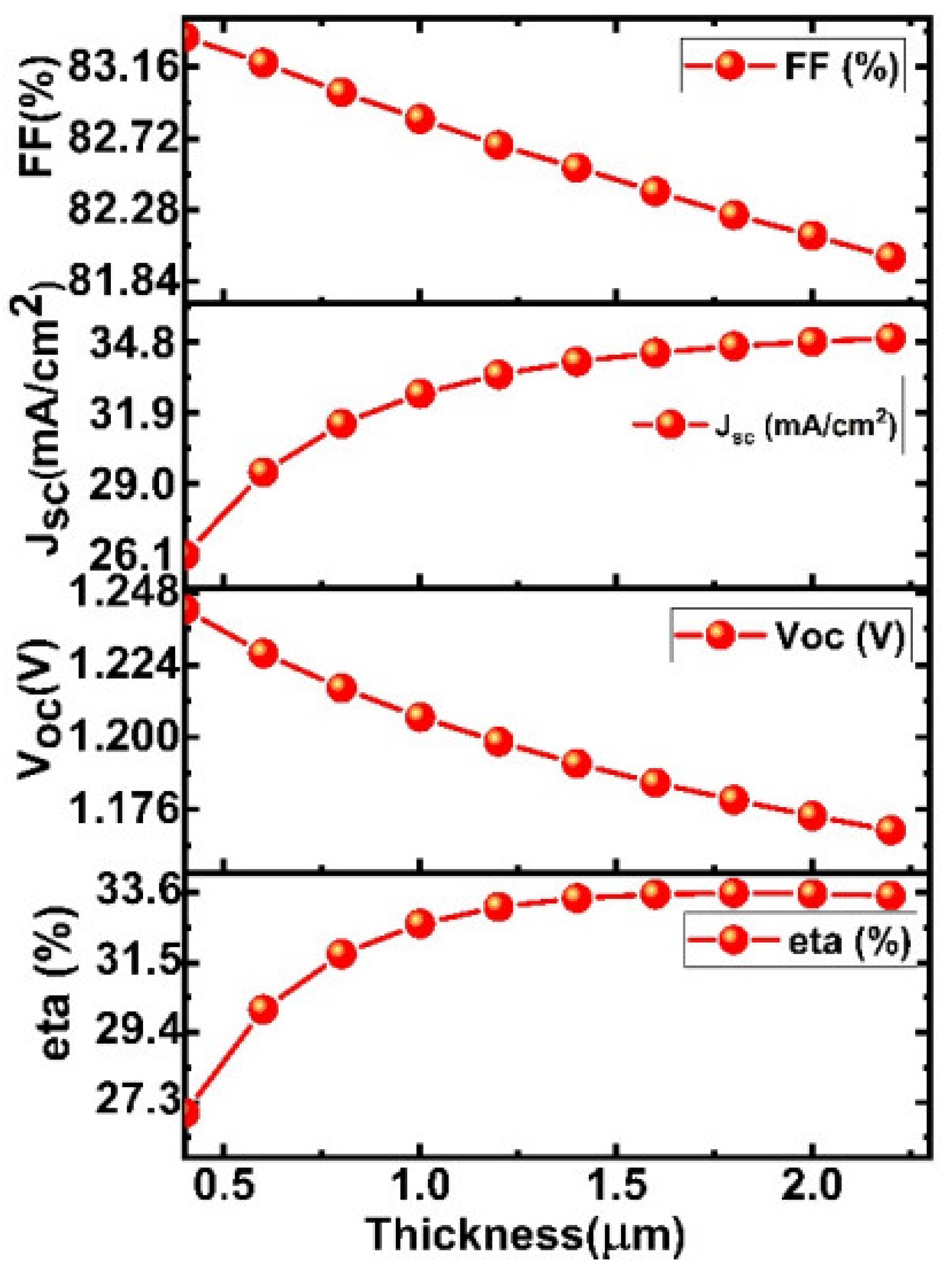
2.6. Performance Properties of Organic Solar Cells

The important electrical characteristics of OSC that are correlated to its performance are the open-circuit voltage, short-circuit current, maximum power point, fill factor, power conversion efficiency, and quantum efficiency. The expected values and interdependence of these parameters are demonstrated on a classical current–voltage (IV) curve (Figure 4).
The maximum possible voltage that can be generated by a photovoltaic (PV) cell is termed as open-circuit voltage (VOC). It refers to difference between the HOMO of the donor and the LUMO of the acceptor material.
V O C = 1 e E H O M O d o n o r E L U M O a c c e p t o r 0.3
Current flowing in the absence of any external resistance (0 voltage) through an illuminated solar cell is termed as short-circuit current (ISC). It refers to the maximum possible current produced by the device. The point of the current voltage characteristic curve (IV) curve that renders the maximum rectangle area is termed as the maximum power point (PMP). At a maximum current and voltage, the ratio of the actual maximum power the output to its theoretical output is termed as the fill factor (FF). The FF is higher for larger inner areas (A), as shown in Figure 4.
F F = P M P   ·   I M P V O C   ·   I S C = a r e a   A a r e a   B
The power conversion efficiency (PCE) is undoubtedly the most important parameter of performance of any OSC. It is a ratio of the output of OSC to the input of energy from sunlight. The abovementioned parameters from the IV curve are used to calculate the PCE, where Pin is the irradiance value.
P C E = I S C   ·   V O C   ·   F F P i n  
Quantum efficiency (QE) is the efficiency of the device as a function of the incident radiation wavelength.

2.7. Efficiency Highlights

Generally, organic compounds are considered to be non-conductors. The discovery of conducting polymers was a breakthrough in this context. Recently, conjugated polymers have gained significant attention is OSC technology since they can act as electron donors in the active layer of OSC. Tandem solar cells prepared by a bulk heterojunction possessing complementary absorbing materials have achieved better performance compared with single cells. Easy processing, low entropy of mixing, and efficient exciton dissociation are the major advantages associated with polymer solar cells compared with small-molecule solar cells. In this section, we briefly discuss the important highlights of the maximum efficiency achieved by OSC.
P3HT is a classical donor conjugated polymer which show comparatively low PCE. A significant improvement in the PCE and other performance parameters for a P3HT-based OSC was recently reported as the introduction of additives [99]. P3HT was used as the donor with 2,2′-((2Z,2′Z)-((12,13-bis(2-butyloctyl)-3,9-diundecyl-12,13-dihydro-[1,2,5]-thiadiazolo [3,4-e]thieno [2″,3″:4′,5′]thieno [2′,3′:4,5]pyrrolo [3,2-g]thieno [2′,3′:4,5]thieno [3,2-b]indole-2,10-diyl)bis(methane-lylidene))bis(5,6-dichloro-1H-indene-1,3(2H)-dione) (ZY-4Cl) as the acceptor while using SA4 as a sloid additive. The additive caused enhanced molecular packing and phase separation, which ultimately resulted in an augmented charge transport and the reduced recombination of carriers. The VOC, ISC, FF, and PCE of the manufactured dev ice were found to be 0.90 V, 17.0 mA/cm2, 0.67, and 10.24%, respectively.
The OSC composed of bithienyl-benzodithiophene-alt-fluorobenzotriazole copolymers/ITIC indicated remarkably high ISC, VOC, FF, and PCE of 17.43 mA/cm, 0.89 V, 0.64, and 9.53%, respectively [100]. The same group demonstrated an improvement in the OSC performance by changing the acceptor material [101]. Herein, the authors introduced meta-alkyl-phenyl substitution on ITIC. While using bithienyl-benzodithiophene-alt-fluorobenzotriazole copolymers as the donor and substituted ITIC (m-ITIC) as the acceptor, a significant improvement in the performance parameters was achieved. A higher PCE of 11.7% along with a VOC of 0.912 V, FF of 0.70, and ISC of 18.31 mA/cm2 was shown by the reported OSC device.
In this context, a new conjugated polymer donor and small molecule acceptor were synthesized, namely, Poly[(2,6-(4,8-bis(5-(2-ethylhexylthio)-4-fluorothiophen-2-yl)-benzo [1,2-b:4,5-b′]dithiophene))-alt-(5,5-(1′,3′-di-2-thienyl-5′,7′-bis(2-ethylhexyl)benzo [1′,2′-c:4′,5′-c′]dithiophene-4,8-dione)] (PBDB-T-SF) and 3,9-bis(2-methylene-((3-(1,1-dicyanomethylene)-6,7-difluoro)-indanone))-5,5,11,11-tetrakis(4-hexylphenyl)-dithieno [2,3-d:2′,3′-d′]-s-indaceno [1,2-b:5,6-b′]dithiophene (ITIC-4F) by Hou and co-workers [102]. The OSC based on PBDBT-SF:IT-4F possessed significantly higher ISC (20.50 mA/cm2), VOC (0.88 V), FF (0.719), and PCE (13%). Moreover, a single-junction OSC made of poly[(2,6-(4,8-bis(5-(2-ethylhexyl)thiophen-2-yl)benzo [1,2-b:4,5b′]dithiophene)-co-(1,3-di(5-thiophene-2-yl)-5,7-bis(2-ethylhexyl)benzo [1,2-c:4,5-c′]dithiophene-4,8-dione)] (PBDB-T) as the donor and 3,9-bis(2-methylene-((3-(1,1-dicyanomethylene)-6/7-methyl)-indanone))-5,5,11,11-tetrakis(4-hexylphenyl)-dithieno [2,3-d:2′,3′-d′]-s-indaceno [1,2-b:5,6-b′]dithiophene (ITIC-M) as the acceptor achieved a PCE of 12.05% [103]. The values of VOC, ISC, and FF of the fabricated OSC were found to be 0.94 V, 17.44 mA/cm2, and 0.735, respectively.
Possibilities of improvements in the multijunction efficiency based on the design principles were demonstrated by combining tandem with a solution-processed non-fullerene-acceptor-based infrared-absorbing subcell on a visible-absorbing fullerene-based subcell [104]. A high PCE of 15% along with a Voc of 1.59 V, Isc of 13.3 mA/cm2, and fill factor of 0.71 were achieved. The effect of regioregularity of the backbone and the fused-ring core modulation of the polymer acceptor on the performance of OSC was demonstrated by Fu and co-workers [105]. The OSC was fabricated using PBDB-T as the donor with a new class of polymeric acceptor benzotriazole (BTz)-core fused-ring segment. A maximum PCE of 15.8% was achieved for the regioregular acceptor (PZT-γ)-based OSC in addition to an enhanced Isc, VOC, and FF of 24.7 mA/cm2, 0.896 V, and 0.71, respectively. The application of a novel polymer acceptor, PYT-1S1Se, an asymmetrical selenophene-fused backbone, while using Poly[(2,6-(4,8-bis(5-(2-ethylhexyl-3-fluoro)thiophen-2-yl)-benzo [1,2-b:4,5-b′]dithiophene))-alt-(5,5-(1′,3′-di-2-thienyl-5′,7′-bis(2-ethylhexyl)benzo [1′,2′-c:4′,5′-c′]dithiophene-4,8-dione)] (PBDB-TF) as the donor polymer was able to achieve a high PCE, VOC, ISC, and FF of 16.3%, 0.926 V, 24.1 mA/cm2, and 0.73, respectively [106]. The development of novel polymeric acceptors by polymerizing an efficient small-molecule acceptor, 2,2′-((2Z,2′Z)-((12,13-bis(2-ethylhexyl)-3,9-(2-butyloctyl)-12,13-dihydro-[1,2,5]thiadiazolo [3,4-e]thieno [2″,3″:4′,5′]thieno [2′,3′:4,5]pyrrolo [3,2-g]thieno [2′,3′:4,5]thieno [3,2-b]indole-2,10-diyl)bis(methanylylidene))bis(5,6-difluoro-3-oxo-2,3-dihydro-1H-indene-2,1-diylidene))dimalononitrile (L8-BO) and its subsequent OSC device manufacturing with PBDB-TF as the donor, was demonstrated by Sun and co-workers [107]. The fabricated all polymer-OSC devices achieved a Voc of 0.949 V, Jsc of 23.73 mA/cm2, FF of 0.74, and PCE of 16.76%.
An effective strategy for improvement in the performance of OSC is additive engineering. However, only limited concentrations of traditional additives can be incorporated, such as 1,8-diiodooctane (DIO) or 1-chloronaphthalene (CN) along with an induced lower stability. Moreover, additional thermal treatment is required, which is an obvious hurdle for industrial applications. In this context, 1,3-diiodobenzene (1,3-DIB) has proved to be a versatile and effective solid additive [108]. A NFA thiadiazolo [3,4-e]thieno [2″,30′:4′,50]thieno [20,30:4,5]pyrrolo [3,2-g]thieno [20,30:4,5]thieno [3,2-b]indole-2,10-diyl)bis(methanylylidene))bis(5,6-difluoro-3-oxo-2,3-dihydro-1H-indene-2,1-diylidene))dimalononitrile (Y6) has gained considerable interest recently. The incorporation of 1,3-DIB in PDBD-TF:Y6 resulted in an improvement in Voc, Jsc, FF, and PCE from 0.87 V, 25.08 mA/cm2, 0.71, and 15.36% to 0.85 V, 26.0 mA/cm2, 0.76, and 16.90%, respectively. All-polymer OSCs have gained significant attention recently. A ternary-all-polymer OSC composed of PDBD-TF as the donor along with a combination of poly[(2,2′-((2Z,2′Z)-((12,13-bis(2-octyldodecyl)-3,9-diundecyl-12,13-ihydro [1,2,5]thiadiazolo [3,4e]thieno [2″,3″:4′,5′]thieno [2′,3′:4,5]pyrrolo [3,2-g]thieno [2′,3′:4,5]thieno [3,2-b]-indole-2,1′-diyl)bis(methanylylidene))bis(3-oxo-2,3-dihydro-1H-indene-2,1-diylidene))dimalononitrile-alt-2,5-thiophene)] (PYT) and a novel fluorinated polymer named PY2F-T as the acceptor had Voc, Isc, FF, and PCE of 0.90 V, 25.2 mA/cm2, 0.76, and 17.2%, respectively. A new donor–acceptor polymer where donor D18 was connected to a fused ring acceptor DTBT was proposed for the improvement of the OSC performance [109]. The single-junction OSC based on D18:Y6 demonstrated a PCE of 18.22% owing to its high hole mobility and wide band gap of D18.
The improvement in the performance by the incorporation of additives has gained considerable interest. Two volatile solid additives (SADs) are designed according to their conformation; SAD1 is a twisted-type while SAD2 is a planar-type [110]. The effect of the conformation of the additive is evaluated by using it with PDBD-TF as the donor and either 2,2′- [[12,13-Bis(2-butyloctyl)-12,13-dihydro-3,9-dinonylbisthieno [2″,3″:4′,5′]thieno [2′,3′:4,5]pyrrolo [3,2-e:2′,3′-g][1–3]benzothiadiazole-2,10-diyl]bis[methylidyne(5,6-chloro-3-oxo-1H-indene-2,1(3H)-diylidene) ]]bis[propanedinitrile] (BTP-eC9) or L8-BO as the acceptor material. In all cases, the performance properties improved compared with OSC without additive. However, planar-type SAD (SAD1) had the best performance, owing to its better insertion in the constituents of OSC. The best-performing device (PDBD-TF:L8-BO-SAD2) achieved Voc, Isc, FF, and PCE of 0.889 V, 26.73 mA/cm2, 0.79, and 18.85%, respectively.
Selectivity in the fabrication process can have a significant effect on the performance of OSC. A binary OSC device composed of Poly[(2,6-(4,8-bis(5-(2-ethylhexyl-3-chloro)thiophen-2-yl)-benzo [1,2-b:4,5-b′]dithiophene))-alt-5,5′-(5,8-bis(4-(2-butyloctyl)thiophen-2-yl)dithieno [3′,2′:3,4;2″,3″:5,6]benzo [1,2-c][1,2,5]thiadiazole)] (D18) as the donor and L8-BO as the acceptor material is used for the evaluation of fabrication process [111]. Sequential deposition resulted in higher performance properties compared with blend heterojunction. OSCs prepared by blend casting had Voc, Isc, FF, and PCE of 0.911 V, 26.31 mA/cm2, 0.76, and 18.14%, respectively, compared with 0.918 V, 26.86 mA/cm2, 0.77, and 19.05% for the OSC prepared by sequential deposition. A combination of an asymmetric selenium-substituted pseudosymmetric electron acceptor, BS3TSe-4F, and Y6 acceptors with D18 as the donor had a record high efficiency of OSC [112]. The fabricated device possessed Voc, Isc, FF, and PCE of 0.845 V, 29.41 mA/cm2, 0.77, and 19.03%, respectively.
Suppressing the charge recombination along with improving charge extraction are critically important for the performance of any OSC. Peng and coworkers reported an improvement in the abovementioned properties by the combination of side-chain engineering of new nonfullerene acceptors (NFAs) in a ternary blend along with a volatilizable solid additive [113]. Thes hindrance of BTP-Th in molecular packing and phase separation is reduced by fluorination of side chains making BTP-FTh. The donor used in this case was Poly [[6,7-difluoro[(2-hexyldecyl)oxy]-5,8-quinoxalinediyl]-2,5-thiophenediyl ]] (PTQ10). An OSC composed of PTQ10 as the donor and binary blend of acceptor materials BTP-FTh:IDIC (0.8:0.2) along with dithieno [3,2-b:2′,3′-d]thiophene (DTT) as additive rendered Voc, Isc, FF, and PCE of 0.870 V, 27.17 mA/cm2, 0.81, and 19.05%, respectively.
Most recently, a record high PCE was reported by Hou and coworkers for a tandem organic solar cell through the introduction of an interconnecting layer composed of electron-beam-evaporated TiOx and PEDOT:PSS [114]. The two sub-cells were PBDB-TF:GS-ISO/TiO1.76 and TiO1.76/PEDOT:PSS, where an efficient electron extraction and low Schottky barriers were obtained due to control of O2 flux during evaporation. For the first time, a PCE of more than 20% was obtained by any OSC. The archived Voc, Isc, FF, and PCE of the best device were 2.01 V, 13.14 mA/cm2, 0.77, and 20.27%, respectively. The study opens a new era of 20% PCE in OSC technology.

2.8. Commercialization Perspective

Efficiency and stability enhancement of OSC are the major challenges in the commercialization of OSC. For improvements in efficiency, several approaches are employed, such as broadening in the absorption of the solar light spectrum, exciton diffusion/dissociation, transport of charges, and collection of charges. On this front, organic materials with broad absorption ranges have been used, and tandem structures of materials have complementary absorption spectra. Improvement in the diffusion/dissociation efficiency can be improved by bulk heterojunction. The formation of nanoscale morphologies can improve the charge transport and charge collection. Moreover, inverted configurations cause interface stability and the degradation of the device and hence improve the overall stability of OSC.
In the last decade, significant progress has been made in the field of OSC. Material design and chemistry of the input materials along with fabrication techniques are the major fronts to address in the context of commercialization. In the last couple of years, a major breakthrough in OSC technology was the achievement of more than 20% PCE. Thickness-intensive photovoltaic properties, high performance, air-insensitivity, green solvents, and no requirement of extra treatment are the required features in the context of commercialization. All of these features must be addressed well from a commercialization perspective. All-polymer OSCs are stable, use green solvents, and achieve a fairly high efficiency that makes them promising candidates for commercialization. Moreover, the introduction of a high-performance interface layer between the complementary sub-cells of tandem OSCs is a promising approach to achieve high efficiency. Generally, photovoltaic materials have complex chemistry and hence are expensive. The exploration of low-cost photovoltaic materials is one of the major interests in context of commercialization. The applications of OSC in portable devices and building-integrated materials will be a great evolution, and we anticipate OSC may constitute a major share in the future of commercial products for renewable solar energy generation [115].

2.9. Recommendations and Suggestions for Improvement and Future Works

Improved OSC efficiency and higher OSC stability are essential for commercial applications. Utilizing tandem solar cells, molecularly tailored donor and acceptor materials, and low-band-gap donor materials can increase the efficiency. Future research should be focused on device stability in areas such as (i) the development of new polymer donor materials with balanced rigidity/flexibility and crystallinity/amorphism properties to simultaneously improve photo/air, thermal, and mechanical stabilities; (ii) the use of non-fullerene acceptors in place of PCBM for better photo/air, thermal, and mechanical stabilities; (iii) developing a comprehensive understanding of OSC device degradation mechanisms with oxygen, water, and irradiation; (iv) the creation of a universal standard for OSC stability tests; (v) the enhancement of OSCs in PCE based on polymers with cleavable side chains and photo/air-stable units; and (vi) the creation of a sophisticated, encapsulating technology for OSCs. The PCE of OSCs have already exceeded 21%; however, stability issues are still a concern in context of commercialization.

2.10. Computational for Organic Solar Cells

The process of synthesizing new materials for OSCs is time-consuming and expensive. Consequently, a computer model for predicting the PCE of a new device without physical experiments is required. The Scharber equation can predict the PCE of any OSC using a few key parameters that can be determined computationally through density functional theory (DFT) and machine learning (ML). The Harvard Clean Energy Project Database (CEPDB) contains computationally predicted PCE values for 2.3 million potential organic photovoltaic systems through machine-learning models.
In this context, the PCE, the short-circuit current density Jsc, the open-circuit voltage Voc, the HOMO energy, the LUMO energy, and the HOMO−LUMO gap are reported as computed by the DFT methods described by Hachmann and co-workers using the Scharber equation.
PCE = FF   V o c J s c P i n
where FF is the fill factor and Pin is the input power.
The open-circuit voltage given by the expression below is derived by Scharber and co-workers.
( V o c = 1 e E donor HOMO E acceptor LUMO 0.3
where “e” is the electron charge, “EdonorHOMO” is the energy of the highest occupied molecular orbital (HOMO) of the donor material in the cell, “EacceptorLUMO” is the energy of the lowest unoccupied molecular orbital (LUMO) of the acceptor material in the cell, and 0.3 is an empirical correction.
The short-circuit current density is given by
J s c = EQE   × e   E g ph E   d E
where the external quantum efficiency EQE set to 0.65 in the Scharber model, Eg is the band gap of the donor material, and ϕph is the incident solar photo flux density as a function of energy E.

3. Perovskite Solar Cells

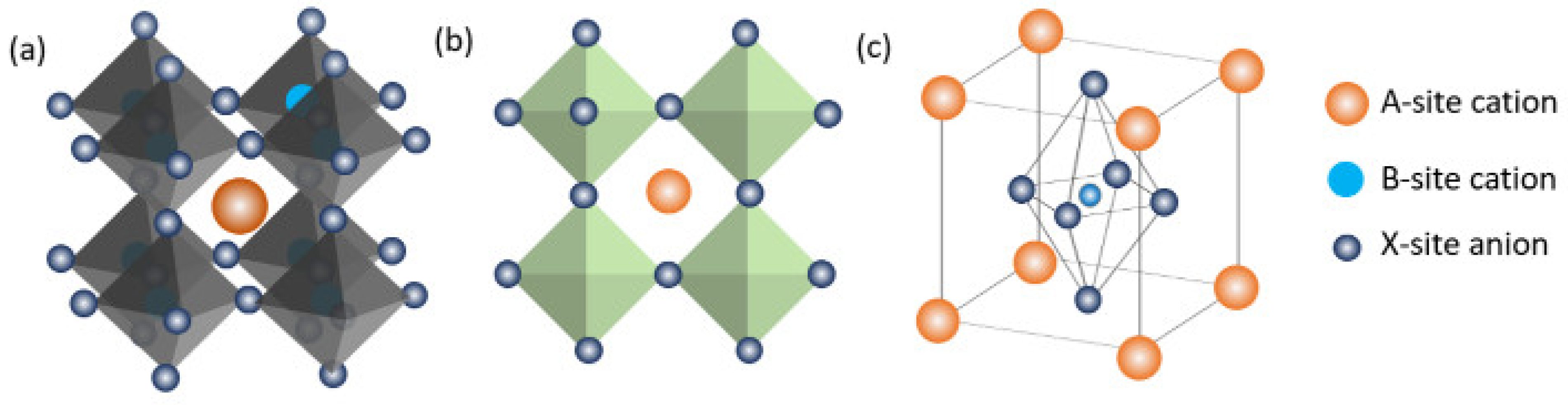
3.1. The Meaning of Perovskite

Originally, the term “perovskite” referred to the calcium titanate crystal structure, which was identified in 1839 by German mineralogist Gustav Rose and given the name by Russian mineralogist Lev Perovski. Compounds with perovskite structures typically contain the formula ABX3, where ‘A’ and ‘B’ stand for cations and ‘X’ is an anion joining the two cations. These metal halide perovskites, consisting of lead (Pb2+), methyl-ammonium CH3NH3+, an organic cation, and a halide anion such as iodide (I) or bromide (Br), have drawn much attention as prospective perovskite solar-cell materials in recent years. Figure 5 displays three-dimensional (3D) and two-dimensional (2D) schematic designs as well as the usual unit cell arrangement of a perovskite compound. Usually, structures can be built from a wide variety of unique component combinations. By changing the composition of these substances, researchers may produce perovskite crystals with a variety of properties, including physical, optical, magnetic, and electrical.
In 1958, Chr. Kn. Moller first discovered halide perovskites for cesium lead halides [117]. Following this, it was also observed that small organic molecules with effective radii less than 260 pm (such as MA (CH3NH3), FA (CH(NH)2)) could also accommodate the inside of the lead halide octahedrons from the analysis of Goldschimdt’s tolerance factor/octahedral factor; additionally, Dieter Weber, in 1978, successfully synthesized MAPbX3 (X = halogens (I, Br, Cl or Mixtures of them) and superhalogen (BF4, PF6)) for the first time [118]. Thereafter, researchers started working on layered 2D perovskite systems (commonly, (R-NH3)2MX4), where the extended inorganic lead halide octahedral cage is separated by large organo-ammonium cations [119]. The resurgent hybrid perovskite was initiated by the introduction of three-dimensional hybrid perovskites (CH3NH3PbI3 and CH3NH3PbBr3) as absorbers [120] in mesoporous solar cells by Miyasaka and co-workers in 2009. Since then, researchers across the globe have used them as absorber materials in photovoltaic cells and achieved PCE as high as 25.7% in sa ingle junction [121] and 29.8% in monolithic perovskite/Si tandem solar cells (Figure 6). Superior optoelectronic properties such as low bandgap with direct nature, high optical absorption both in visible and IR regions, ultrahigh diffusion length, high defect tolerance, large and balanced electron-hole mobilities, high photoluminescence quantum yield, and low surface recombination velocity make them attractive candidates for solar-cell application [122,123].
Nowadays, the various structures of perovskite solar cells such as mesoporous, planar, and inverted structures have been developed. In the mesoporous solar cells, the device structure was composed of glass/fluorine-doped tin oxide (FTO)/dense electron transport layer (ETL)/mesoporous oxide layer/perovskite layer (~500 nm)/hole transport layer (HTL)/metal electrode [124,125,126]. The mesoporous TiO2 is used as an ETL material allowing perovskites to penetrate into the pores to form an interconnected absorbing layer. Additionally, titanium dioxide (TiO2) also prevents the electron-hole recombination in the FTO by blocking the holes. Experimental results revealed that other oxide materials such as zinc oxide (ZnO), aluminum oxide (Al2O3), and zirconium dioxide (ZrO2) were also used as mesoporous oxide layers. In this structure, Spiro-OMeTAD (2,2′,7,7′-Tetrakis [N, N-di(4-methoxyphenyl) amino]-9,9′-spirobifluorene) is the most used HTL and noble metals such as Au, Ag, and Pt are used as the counter electrodes. In the case of planar structure, the mesoporous ETL is removed and only two sharp interfaces are observed between perovskites and two transport layers (ETL and HTL). As a result, the rapid and effective separation of electrons and holes are observed through the ETL and HTL, respectively [127]. Due to the minimum number of interfaces, planar heterojunction structures help to understand the operating mechanisms of light absorption and electron-hole separation precisely and optimize the structure for the development of highly efficient laminated perovskite photovoltaic cells. Besides the two abovementioned structures, perovskite solar cells without HTL have become an interesting research project due to their advantages of easy and simple device fabrication and high stability [128]. These perovskite materials served the purpose of both light absorbers and hole transport channels. Using device simulation, Minemoto and Murata showed that the built-in electric field was not affected if the work function of metal electrodes was close to the valence band maximum of the light-absorbing materials for the case of HTL-free perovskite solar cells [129].
Usually, the perovskite layer is spin-coated on the substrate via either a single-step or two-step process. In the single-step process, perovskite precursor (a mixture of CH3NH3I and PbI2 dissolved in DMF:DMSO) is spin-coated onto the FTO substrate in one step and kept at 1000 C to achieve a uniform perovskite film. In recent times, an anti-solvent method is effective, in which the perovskite precursor solution is prepared in the polar solvent and quenched during the process of spin coating by a non-polar solvent. It is often observed that precise control over the volume of quenching solvent and timing is very much essential to achieve uniform morphology and optimal device performance. In the two-step process, lead iodide (PbI2) was the first to be spin-coated and then transferred into a vessel where 1 molar CH3NH3I was dissolved in isopropanol. Other than these two frequently used methods, OIHPs can also be deposited via a ‘vacuum-assisted solution process’ (VASP) in which perovskite films are coated and annealed in a chamber filled with the organic component vapor [130].

3.2. Advantages and the Challenges of Perovskite Solar Cells

Perovskite photovoltaics have a high light-absorption coefficient (104 cm−1), which results in an impressive photocurrent generation [131], long carrier diffusion length, and solution processability [132,133,134]. Perovskite solar cells are cheaper to produce, owing to their inexpensive and naturally abundant materials (lead, iodine, carbon, and hydrogen) [135]. These solar cells show better defect tolerance than other solar semiconductors on the market [136], which increases their reusability and lowers production costs. Despite their benefits, the commercialization of perovskite solar cells is hampered by another factor. Water by itself (moisture) and other polar solvents provide a serious problem for perovskite solar cells. These solvents can alter the solvated phases of a perovskite and occasionally hydrate a perovskite to produce a monohydrate phase. Polar solvents can considerably be prevented from harming perovskite solar cells by modifying deposition techniques, according to reports. However, environmental moisture is unavoidable [137].
It is observed that various external factors such as oxygen, light, and heat have expedited the degradation, which can be slowed by choosing a proper composition of the perovskite material (such as FA0.85MA0.1Cs0.05PbI2.7Br0.3, which show better stability and power conversion efficiency) [138,139,140,141]. In addition, it was noted that the deposition of more hydrophobic and UV-stable ETL/HTL has improved the stability of the device (replacing TiO2 with SnO2). The combination of Ruddlesden–Popper (RP) 2D-layered perovskites with conventional 3D perovskites has improved the stability of the device as 2D perovskite passivate/encapsulate the device [142].
On the other hand, the use of an excessive amount of lead in the perovskite component is also another big challenge in its commercialization. As an alternative, tin-based perovskites are studied, but the PCE of such devices [143] is poor (PCE ~13%). Current-voltage hysteresis between the forward and reverse bias is another major issue. Although the reason for hysteresis is still under debate, it is commonly ascribed to the combination of ion migration with high levels of charge-carrier recombination. To achieve a truly low cost-per-watt and dominate the photovoltaic market, solar cells based on OIHPs should satisfy the much-heralded trio of high-power-conversion efficiency (PCE), yearlong lifetimes, and ultra-low manufacturing costs. Certainly, OIHP-based solar-cell devices are quite farther ahead than other thin-film technologies, as they have shown enormous potential for achieving this.

3.3. Future Prospective

According to us, future research is likely to focus on the following steps: (i) reduction of halide defect sites through additives and passivation, (ii) the inclusion of 2D perovskites and better-optimized interface materials to increase the efficiency and stability, (iii) the use of inorganic charge-extraction layers rather than organic ones to improve both efficiency and stability, and (iv) proper understanding of charge-carrier transport mechanism.

3.4. The Difficulties and Strategies for Improving Solar Cell Stability

The hydrophilic and volatile nature of organic molecules make hybrid perovskite vulnerable to degradation through humidity and heat, which limits the long-term stability of perovskite solar cells for industrial applications. Several fundamental strategies have been adopted to slow down the degradation of the absorber materials and increase device stability: (i) develop a more resilient perovskite absorber via cation substitution/doping; (ii) controlling perovskite crystallization by novel approaches such as solvent engineering and the use of additives or non-halide, (iii) using carbon-based functional materials such as carbon nanotubes (CNT), graphene, or fullerene (C60) between the perovskite absorber and the hole-transport materials, and (iv) developing a protective layer (encapsulation technique) around the absorber material. To date, most perovskite solar cells with high stability are inverted (p-i-n) type (maintaining >90% of the initial power conversion efficiency over 1000 h).

3.5. Current Progress of Tandem Solar Cells

A steep absorption edge, exceptionally low sub-gap absorption, tunable bandgap (by changing halide composition), and desirable Voc of 1.15 V corroborate the hybrid perovskite as a suitable candidate for top wide-bandgap cells in the tandem configuration. Furthermore, the low-temperature fabrication of perovskite helps to monolithically integrate it as a top cell without damaging the bottom cell. A high power-conversion efficiency (PCE) of 32.5% and 29.8% has been achieved in monolithic 2T and 4T perovskite/silicon tandem solar cells, where perovskite was used as the top sub-cell and silicon as the bottom cells, respectively. Other than the above, various perovskite-based tandem cells such as perovskite/CZTSSe (PCE~14.2%), perovskite/CIGS (PCE~26.8%), perovskite-DSSC (PCE~17.5%), and perovskite-perovskite (PCE~25.9%) have been widely developed in recent years and will be ready for commercialization within a couple of years.

3.6. Commercialization of Solar Cells

Irrespective of the high power-conversion efficiencies of Si, CIGS, and CZTSSe-based solar cells, high manufacturing costs and limitations in large-scale production are considered as major drawbacks for further versatile applications. Thus, various types of lost-cost solar cells such as small-organic molecule/polymer-based solar cells, dye-sensitized solar cells are being investigated aiming to replace Si-based solar cells. Recently, hybrid perovskite solar cells are considered as a potential replacement for Si-based solar cells due to their low production cost, high power conversion efficiency, lightweight, and possibility of flexible device fabrication. Yes, it is true that stability of perovskite solar cells is the major drawback, which pales in comparison to the 25-year stability of silicon. The longest reported lifetime for the prototype single-junction perovskite solar cell was 6000 h under continuous one-sun illumination before degrading by beyond 80% of its initial performance. As an alternative of single-junction cells, perovskite–Si tandem cells show better stability. Thus, several companies such as Oxford PV, Hanwha Q Cells, Greatcell Energy, Saule technologies, Quantum Solution, and Energy Materials are in the advanced stages of commercializing perovskite solar cells.

3.7. Lead-Free Perovskite Solar Cells

The study of the properties of lead-free perovskite solar cells has been performed by many researchers. Methylammonium tin iodide (CH3NH3SnI3) could be used to replace lead due to its narrower band gap, eco-friendliness, wider visible absorption spectrum, and excellent mobility. Ahmad and co-workers [144] described a solar cell made from glass/ITO (as an electron-transport layer)/n-type WS2/CH3NH3SnI3/p-type P3HT (as a hole-transporting layer)/Au. Tungsten disulfide (WS2) indicated a small, indirect band gap (1.3 eV), a big direct band gap value (2 eV), a high carrier mobility, and excellent conductivity. The homo-polymer poly (3-hexylthiophene), called P3HT, showed a wide band gap, high hole mobility, robust hydrophobicity, high thermal stability, and relatively low cost. The experimental findings showed power conversion efficiency (due to number of carriers increased) and the short circuit current density increased (due to more photons falling on it); however, the fill factor and open-circuit voltage reduced (due to an increase in dark saturation current) with the increase in the film thickness (Figure 7). It is noted that more photons were absorbed when the film thickness was increased. These photons could penetrate deeper into the absorber layer, resulting in the production of more electron-hole pairs in devices. The photovoltaic parameters (fill factor = 81.59%, open-circuit voltage = 1.0997 V, power-conversion efficiency = 33.46%, short-circuit current density = 37.17 mA/cm2) were studied under optimized conditions. Nihal and co-workers proposed zinc magnesium oxide (ZnMgO) and MASnBr3 as an electron-transport layer and hole-transport layer, respectively [145]. The photovoltaic behaviors (fill factor = 82.01%, open circuit voltage = 0.95V, power conversion efficiency = 26.33%, short circuit current density = 33.85 mA/cm2) were investigated in specific solar cells (Zn0.75Mg0.25O/CH3NH3SnI3/MASnBr3). Komal and co-workers used ZnTe (as the hole-transport layer) to replace spiro-OMeTAD, which is a very expensive) material [146]. The power conversion efficiency reached 22.96% (simulation model) and 8.41% (fabrication model) based on the experimental results.

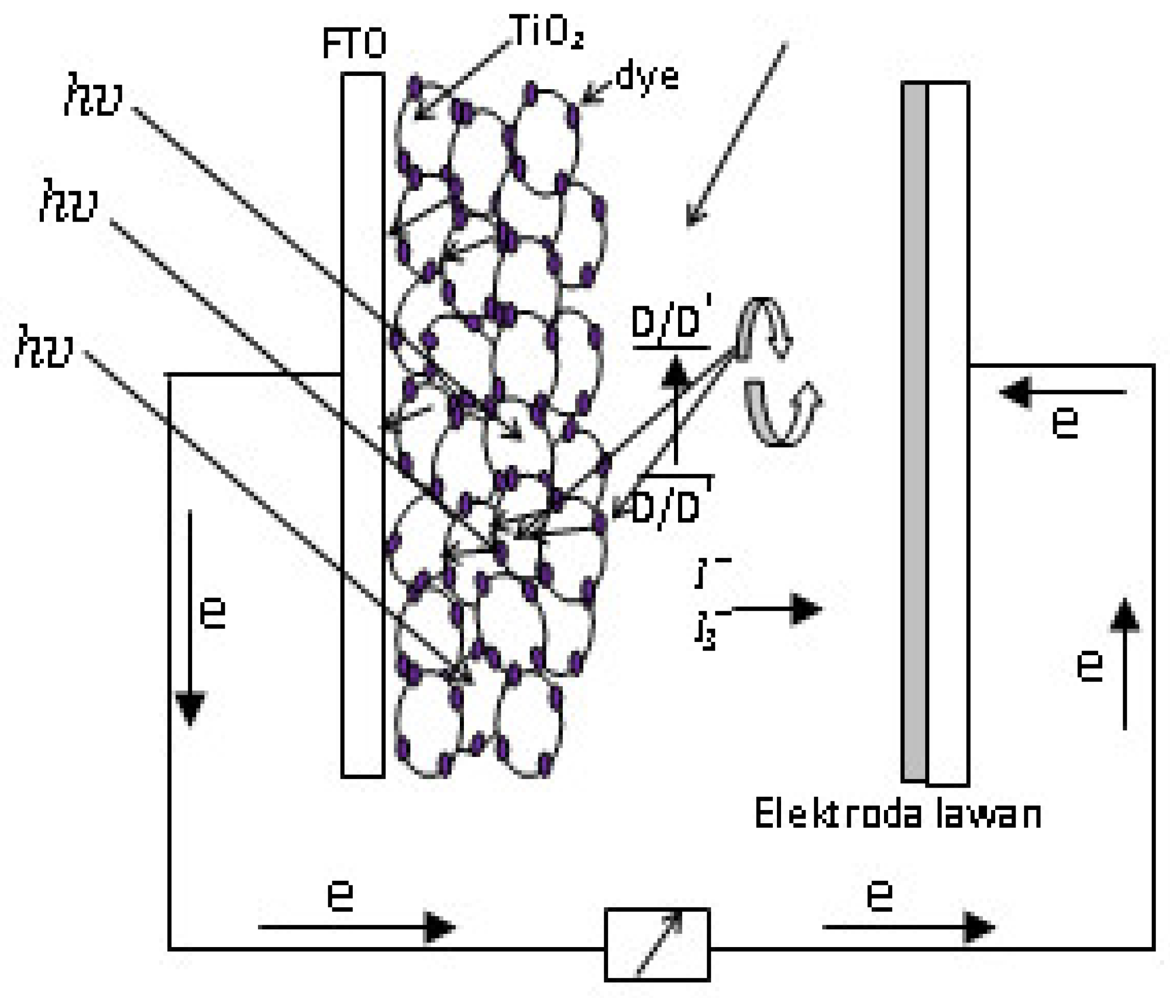
4. Dye-Sensitized Solar Cells

Dye-sensitized solar cells (DSSC) are solar cells made of semiconductors that are coated with a dye to increase the efficiency of sunlight [147]. This type of solar cell was first introduced by Michael Gratzel. DSSCs are composed of a working electrode consisting of fluorine tin oxide (FTO) glass, titanium dioxide (TiO2), dye, an electrolyte consisting of an I¯/I3¯ redox pair, and a counter electrode consisting of platinum. DSSCs work in the visible region. DSSC components have undergone various developments over the years to increase their efficiency.

4.1. Advantages and Limitations of Dye-Sensitized Solar Cells

Some of the advantages offered by dye-sensitized solar cells, including their relatively low cost of fabrication, operability under scattered light conditions, and the variable shape of the cell, which can be made opaque or opaque or optically transparent, thereby providing more value from an artistic point of view [148]. Organic solar cells have dyes derived from organic and synthetic organic materials. Examples of dyes from organic materials are mangosteen, juwet fruit, water henna, nail henna, blueberries, binahong leaves, carrots, kenikir, and mangosteen peel. Synthetic organic dyes such as ruthenium complex (N719) could produce a higher efficiency of 10.4–11.1% [149,150]. However, the cost of producing ruthenium complex dyes is still relatively high, thus encouraging the development of new dye sensitizers (complexes of osmium, rhenium, iron, and iridium) [151].
The advantages of using synthetic, organic dyes include their higher conversion efficiency (an efficiency increase of up to 30% in synthetic dyes, with organic dyes being 5%), increased chemical and thermal stability, the color being difficult to degrade compared with organic dyes, and having a higher electron movement than organic dyes. There have been many studies using natural organic dyes and ruthenium dyes with a wide variety of solvents, including research conducted [152] using nano-particle TiO2 paste, ruthenium dye (N719), and counter electrodes (platinum) to produce the greatest efficiency of 0.121%. Hardani and co-workers [153] made DSSC using TiO2 doping carbon nanotubes with various concentrations and ruthenium (N719) as a dye, and the resulting efficiency was 1.3%. Another research group [154] used TiO2 nanoparticles as the active electrode and ruthenium complex (N719) as a dye and the greatest efficiency reached 2.17%.
The solid electrolyte based on PEG polymer gel (polyethylene glycol) containing redox coupling is used (to replace liquid electrolyte) to reduce electrolyte degradation. During the experiment, the doctor blade/slip-casting and spin-coating techniques were used for TiO2 coating. In comparison with other processes, this doctor blade/slip-casting method is incredibly straightforward and uncomplicated. The spin-coating technique is used to deposit homogeneous thin films on a flat substrate. While, the doctor blade/slip-casting technique is a technique for coating the TiO2 suspension on semiconductor glass utilizing a stir rod/spatula by rolling it on the glass surface to flatten the dripping TiO2 suspension. The substrate’s center, which either rotates slowly or not at all, receives a modest amount of coating material. The coating substance is subsequently dispersed throughout the substrate using centrifugal force as the substrate is rotated quickly. The device used for spin coating is called a “coater” or “spinner”. Spin coating is a straightforward TiO2-deposition technology that produces films with regulated thickness and great uniformity by rotating the TiO2 paste at a specific speed.

4.2. Definition and Fundamental of Dye-Sensitized Solar Cells

DSSC generally uses indium tin oxide (ITO) or fluorine-doped tin oxide (FTO) as a substrate. The oxide substrate layer functions as a current collector and the substrate material itself as a sealing layer between the cells in the DSSC and the outside air [155].
Titanium dioxide (TiO2) is the material of choice used as a working electrode or photoelectrode in DSSC. The three modifications of TiO2 include anatase, rutile, and brookite, but only anatase and rutile are stable [156]. Brookite is difficult to produce and therefore is not considered in DSSC applications [157]. The particle sizes of anatase and rutile increase[158] with increasing temperature. Figure 8, showing different growth rates, shows that rutile has a much higher growth rate than anatase. The growth rate of anatase is flat at 800 °C.
The absorbance spectrum defines the possibility of a useful semiconductor for photocatalysts having a band gap (Eg) proportional to the photon energy of the visible or ultraviolet spectrum (Eg < 3.5 eV). Most authors have determined that the energy gap of rutile is 3.0 eV and that of anatase is 3.2 eV. A larger active surface area and a more effective photocatalyst [159] can be observed in the anatase phase.
The photocatalytic process is based on the dual ability of a semiconductor material (TiO2) to absorb photons and carry out transformation reactions at the material junction simultaneously. Figure 9 shows several photoexcitation pathways [160] followed by electron and hole de-excitation. The enlarged portion of Figure 9 shows electrons excited from the valence band (Ev) to the conduction band (Ec) due to photons with energy (hv) equal to or greater than the band gap of the semiconductor.
From Figure 9, it is assumed that the semiconductor remains intact, and the charge transfer is uniform to the adsorbed organic or inorganic molecules. The excited electron-hole pair can go through several paths as follows: the semiconductor can donate electrons on the surface to reduce the adsorbed acceptor ( A / A ), for example, oxygen (lane c). Holes can migrate to the surface and electrons from donors (D/D+) can join holes (c lanes). Competition for electron transfer to adsorbed molecules by the separate recombination of electrons and holes occurs in the volume of the semiconductor particles (band b) or on the semiconductor’s surface (lane a).
Electron paramagnetic resonance spectroscopy (EPR) showed that the detected electrons were either captured as Ti3+ or as electrons in the conduction band, while the holes were trapped in the O free-oxygen center resulting from the O2− lattice in the valence band. The reaction is written as follows [161]:
e + T i 4 + T i 3 + ( electron trap )
h + + O 2 O ( hole trap )

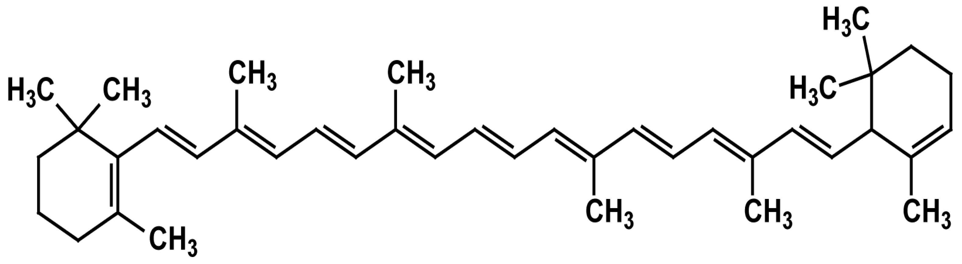
4.3. The Development of Natural Dye from Plant Extracts in DSSCs

Many researchers have developed DSSCs by utilizing various types of natural dyes from plant extracts. Some that have been developed include dye extracts or plant pigments such as chlorophyll extract [162], anthocyanins [163], and beta carotene [164]. One of the results of the DSSC that has been developed [164] by using carotenoids succeeded in making DSSCs with an efficiency of 3% and which were stable after 1 h of sunlight exposure. Beta-carotene is found in every part of the plant, namely from flowers, fruits, stems, and roots, and provides pigments to fruits and flowers with distinctive red, orange, and yellow colors [165]. Plant pigmentation occurs because the structure of the pigment interacts with sunlight to change wavelengths that are either transmitted or reflected by plant tissues [166,167,168].
Carotenoids are involved in photosystems and contribute to energy absorption in the visible light spectrum by transferring the absorbed energy to chlorophyll. Carotenoids also protect from excess light through energy dissipation, the detoxification of free radicals, and limiting damage to cell membranes. In addition, highly conjugated carotenoids can function as short-wire molecules that mediate the electron transfer in donor–acceptor complexes and membranes. Figure 10 shows beta-carotene having a series of delocalizations, but on a larger scale with 11 carbon–carbon double bonds conjugated together [169]. Beta-carotene absorbs the visible light spectrum between 380 and 520 nm. Therefore, it takes less energy to push electrons on beta-carotene than TiO2, which works in the ultraviolet range (<400 nm). The number of conjugated double bonds (CDB), maximum absorption (λmax), and carotenoid colors are presented in Table 1.
The trivial and semi-systematic names of carotenoids are shown in Table 1. The number of conjugated double bonds (CDB) was compared with the maximum absorbance spectra (λmax) and the color of the carotenoid solutions. The maximum absorbance spectra expressed in acetonitrile/ethyl acetate solution were measured using high-performance liquid chromatography (HPLC) with a PDA detector [170] unless otherwise stated. Beta-carotene is one of the most abundant classes of carotenoids found in food and is used as a food coloring. Plants that produce beta-carotene include corn [171], pumpkin, carrots, tomatoes, and melinjo fruit. Schematically the working principle of DSSC is shown in Figure 11. In the simplest arrangement, the DSSC consists of a transparent conductive glass coated with nanocrystalline TiO2 (nc-TiO2), a dye molecule bound to the nc–TiO2 surface, and an electrolyte such as I¯/I3¯, with illuminated cells capable of generating voltages and currents [172].

4.4. Commercialization of DSSC

Dye-sensitized solar cells have attracted increasing attention (cost effectiveness and ease of production) in the last few years. Research is ongoing to improve the efficiency and stability of solar cells. Technically speaking, natural dyes are inefficient and show very weak binding properties with titanium dioxide. Therefore, synthetic dye was used to create the most stable and effective dyes. Based on the analysis, the world DSSC market size was valued at approximately USD 90.5 million, in 2019, and is expected to reach an annual growth rate of 12.4% (from 2020 to 2027). This solar cell could be used in building-integrated photovoltaic, portable charging, automobile, electronic gadgets, and mobile devices. Several factors such as the installation of off-grid solar cells in African countries, the European Union cutting down its carbon emissions, the movement towards renewable energy sources, and enhanced technological development in the solar energy system increase the demand for DSSC.

4.5. Tandem Dye-Sensitized Solar Cells

Researchers have reported that tandem cells could be used to enhance the performance of solar cells. During the experiment, two TiO2 films were put face-to-face (as electrodes), while the platinum mesh sheet was served as counter electrode. The experimental results confirmed that efficiency was increased (from 1.8% to 3.9%) due to the current density being added. Another research group revealed that tandem-structured cells show lower circuit currents and higher open-circuit voltage when compared to conventional DSSC. Technically speaking, tandem design could be divided into three types, namely n-type DSSC + n-type DSSC (higher efficiency could be reached), n-type DSSC + other solar conversion devices (could be employed in industrial applications), and n-type DSSC + p-type DSSC (lower efficiency).

4.6. The Future of DSSC

In the future, DSSC will emerge as an attractive solar energy technology due to its provision of an economical option to p–n junction solar cells. Several research works have been carried out to enhance the efficiency of solar cells. Researchers have reported that light absorption must achieve the highest visible and near-infrared spectrum to gain better efficiency values.

5. Thin-Film Solar Cells

Currently, there are different types of thin-film materials that have been and are employed in solar-cell applications. Technically speaking, these materials have several advantages such as low production cost, being environmentally friendly, and the formation of films can be conducted in various substrates [173].

5.1. CdTe Film Solar Cells

Cadmium telluride (CdTe) films show high degradation durability, near-optimum band-gap value (1.45 eV), a low production cost, and high direct absorption coefficient (104 cm−1), and can be used to replace silicon-based solar cells. Generally, CdTe-based solar cells consist of glass, transparent conducting oxide (serving as the front contact), a CdS window layer, a CdTe absorber layer, and back contact. However, this type of solar cell has many problems such as glass breakage (during the production process) and poor thermal conductivity (causing very poor performance). The preparation of CdTe films onto flexible metal foils and polymer substrate can solve these problems. The power conversion efficiency was shown to be 11% for devices prepared on polyimide foils [174], indicating the superstrate and substrate configurations. Several deposition methods have been reported to produce cadmium-tellurium thin films (Table 2). The photovoltaic properties of the obtained films were studied.

5.2. Cu(In,Ga)Se2 Film Solar Cells

The Cu(In,Ga)Se2 (CIGS) films are already available in the global solar panel market due to their excellent radiation tolerance, high absorption coefficient (105 cm−1), suitable band gap value (1.04 eV to 1.65 eV), and long-term stability. However, these films are very expensive because of the indium and gallium (poor abundance). Several deposition techniques have been reported for the preparation of CIGS films and the photovoltaic parameters were studied as well (Table 3). Thin films could be deposited onto rigid glass substrates, and successfully reached power conversion efficiencies of up to 20.3%. However, the current focus of the production of films onto flexible substrates (metal foils and polyimide films) is because of their significantly lower cost. Polyimide films are highly desirable due to electrical insulation and enabling direct monolithic interconnection.

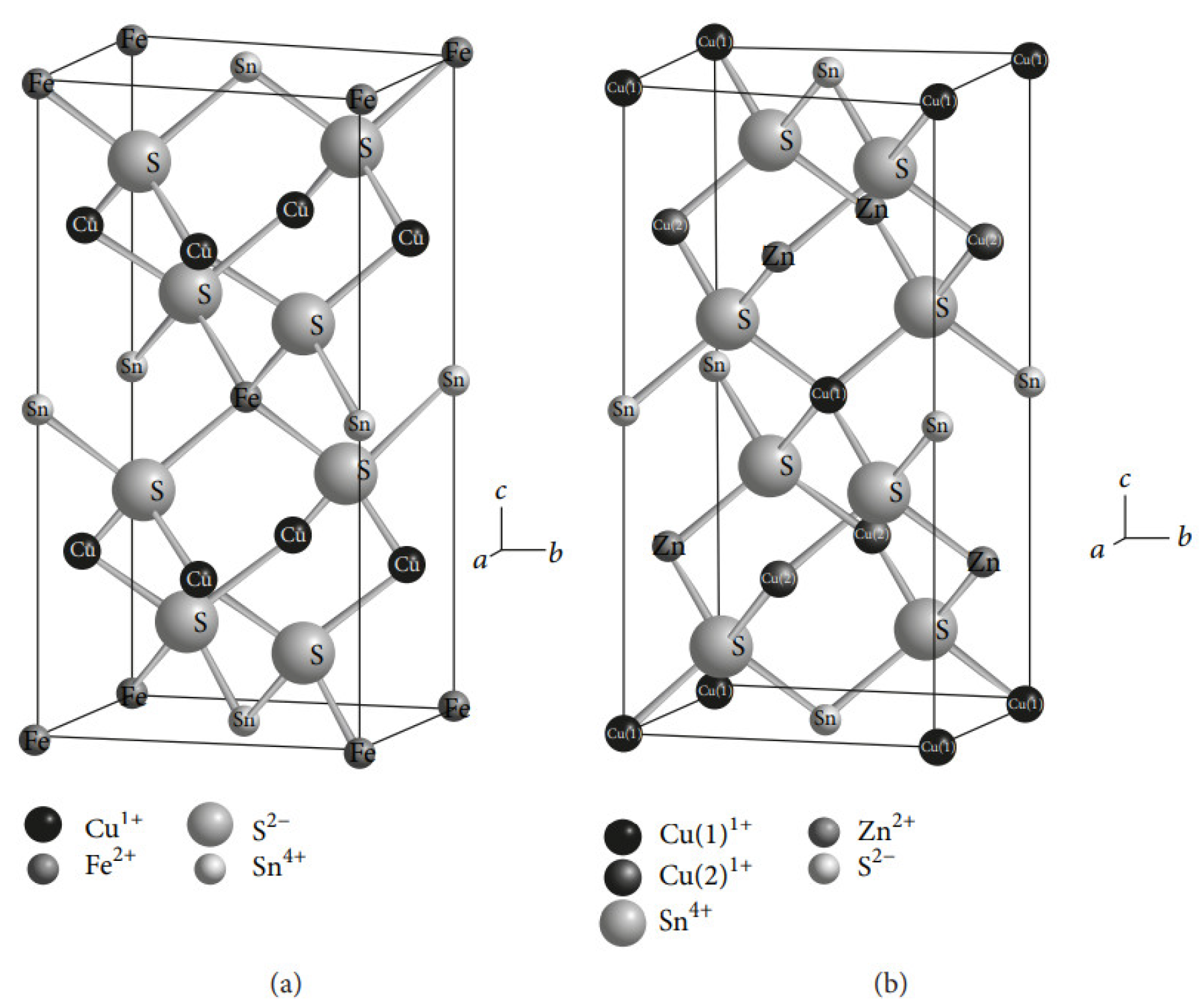
5.3. Cu2ZnSnS4 Film Solar Cells

Copper–zinc–tin sulfide (Cu2ZnSnS4) films are becoming increasingly prominent for several reasons. These materials could replace indium and gallium in CIGS films, as their constituents are Earth-abundant and do not contain cadmium (toxic material). The experimental results showed that CZTS-based solar cells have an excellent absorption coefficients (more than 104 cm−1), tunable band gap values (1.45 eV to 1.6 eV), and greater stability in the kesterite phase (Figure 12) when compared with stannite and wurtzite. Researchers have reported that vacuum and non-vacuum deposition techniques have been used to produce CZTS films (Table 4). Further, they concluded that high-quality films could be synthesized using the vacuum-deposition method; however, this entails increased production costs.

5.4. CuInX (X = S, Se, and Te) Film Solar Cells

Several deposition methods have been used to produce CuInSe2, CuInTe2, and CuInS2 films (Table 5). It is noted that the non-vacuum deposition method offers an attractive cost-saving opportunity, higher deposition speed, and less waste of chemicals when compared with the vacuum-deposition technique. The obtained films could be employed for solar-cell applications because of long-term stability under solar radiation, excellent absorption coefficients (105 cm−1) in the visible light portion, and suitable band gap values (1.5 eV).

5.5. Other Metal Chalcogenide Film Solar Cells

Based on the literature review, several types of metal sulfide, metal telluride, and metal selenide films have been prepared using different deposition methods. The photovoltaic behavior of these films was studied (Table 6) as reported by many researchers.

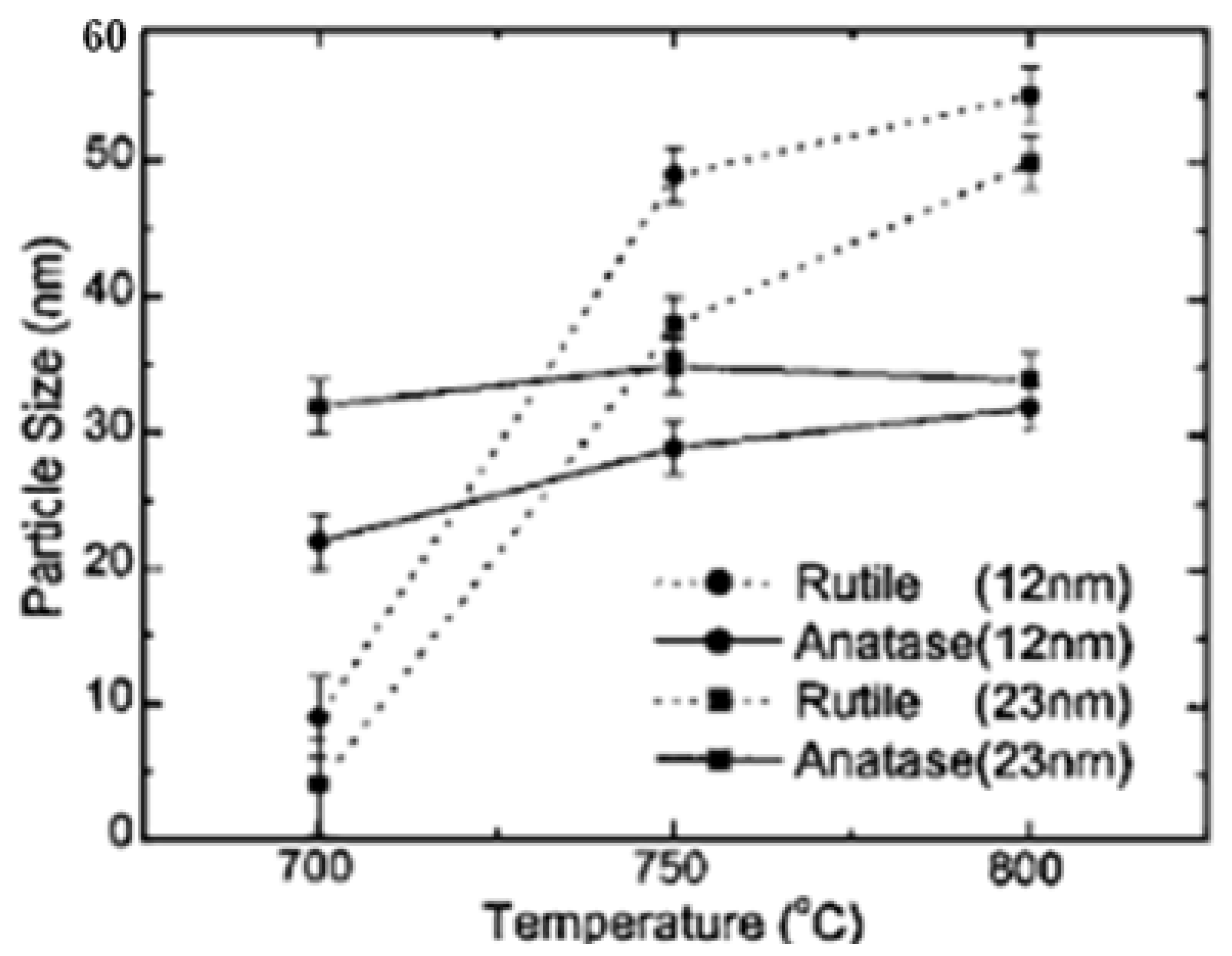
5.6. Quantum Confinement Effect in Thin-Film Materials

Several researchers have reported quantum confinement effects in the obtained nanostructured materials. The chemical precipitation method has been used to produce cadmium sulfide and Gd-doped CdS films [260]. Based on the Raman spectra analysis, 1LO,2LO and 3LO peaks have been moved to lower wavenumbers in Gd-doped CdS films (296, 591, and 896 cm−1) when compared with CdS films (301, 598, and 902 cm−1) because a smaller ionic radius could be observed in Gd (0.94 A) than in cadmium (0.96 A). In addition, they pointed out that the absorption edge had been shifted to a longer wavelength (due to the quantum confinement effect), when compared with CdS based on the optical absorption spectra. Zinc selenide films have been synthesized on glass substrates using the e-beam evaporation method [261]. Experimental results confirmed that the blue shift of the band gap occurred (about 0.16 eV in the thinner films). The band gap increased from 2.62 eV, 2.67 eV to 2.78 eV when the film thickness was reduced from 47 nm, 12.3 nm to 7.9 nm according to optical absorption spectroscopy analysis. The presence of a strong quantum-confinement effect has been reported based on theoretical calculation using the potential morphing method. Azizian and co-workers [262] described the synthesis of SnS films via the ultrasonic irradiation method. The experimental findings showed that the absorption edge had been moved towards the lower wavelength side (blue shift). The particle size and the direct band gap were found to be 4 nm and 1.74 eV (blue shifted when compared with the bulk band gap), respectively. The chemical deposition (spin-coating method) of SnSe (tin selenide) films exhibited size-dependent electronic band gap values [263]. The particle size (10.13 nm to 14.32 nm) and film thickness (1 μm to 4 μm) increased when the band gap was reduced (1.92 eV to 1.51 eV). It was noted that the obtained band gap was higher when compared with bulk value (1.1 eV) because of the quantum confinement effects.

5.7. The Wavelength of Light and Its Effects on the Solar Cells

Solar panels are designed to adsorb sunlight in a particular wavelength range (called a band gap). Usually, these panels are able to absorb light in the visible area (different colors have different amounts of energy). Thin-film solar cells can absorb a wider range of wavelengths (400–1100 nm) when compared with crystalline silicon solar cells (850 nm). Solar panels can produce electricity from sunlight. Photons hit the solar panel and electrons flow through the material and produce an electric current.
Researchers have reported that the highest efficiency strongly depends on the band gap. If the band gap value is too high, most photons do not cause the photovoltaic effect. In contrast, most photons have more energy to excite electrons if the band gap is too low. Currently, the band gap values for CdTe and silicon were found to be 1.5 eV and 1.1 eV, respectively.
Ogherohwo and co-workers [264] highlighted that the wavelengths of light affect the performance of solar cells. The specification of the solar module was reported (maximum system voltage = 8V, short circuit current-238Ma, open circuit voltage = 6.5V, dimensions = 180 mm × 120 mm, weight = 3 kg, temperature co-efficient = 25 °C). Based on Table 7, red color produced the highest power-conversion efficiency when compared with the other colors.

5.8. Future Prospects and Commercialization of Thin-Film Technologies

Based on the analysis, the world thin-film solar cell market size [265] was valued at $11.3 billion (in 2020) and is expected to rise to $25.3 billion (by 2030). Several factors such as the declination of solar price, high electricity demand, and increased solar-cell capacity have contributed to the growth of the market Cadmium telluride films dominate the solar cell market, followed by amorphous silicon and copper indium gallium selenide films. Thin films have been deposited on metal, glass, and plastic. The obtained materials (film thickness) were 20 times lighter when compared with crystalline silicon wafers. In the future, thin-film solar panels could be implemented in the residential industry due to lower installation costs.
Polycrystalline thin-film solar cells could be the most promising candidates for solving the energy production problem due to their low cost in large-scale industrial production and their improved power conversion efficiency. The time-stability should be maintained (within 25 years) in hot, hard conditions. Thickness reduction is needed to optimize the internal resistance (solar cell device) and minimize electrical power loss. In the CuInSe2-based solar cells, efficiency could be improved by reducing the recombination current. Non-hazardous CZTS films could be used to replace CIGS films (indium and gallium are rare). The precise tuning of the band gap (CZTS films) could be carried out by adding some impurities (Ag, Na, Sb). In CdTe-based solar cells, the performance of solar cells could be improved by adding a buffer layer (reducing the shunt-resistance problem).

6. Conclusions

A solar cell is a device that can convert solar radiation into electrical energy. Solar cells are very important develop, considering that the sun supplies a clean and unlimited source of energy. Developing solar cells is one of the most important efforts to save the world from the energy crisis and pollution. This has led many researchers to develop organic solar cells, perovskite solar cells, thin-film-based solar cells, and DSSC solar cells. Several disadvantages of solar cells have been reported by researchers. For example, the commercialization of perovskite solar cells is hampered by lead toxicity and their long-term stability. Currently, the light-induced deterioration of perovskite solar cells under operational conditions (moisture, oxygen, heat, and common stress) is a major problem for outdoor perovskite solar-cell applications. Their efficiency is impacted by the continual breakdown of the MAPbI3 due to exposure to light. Based on the photovoltaic properties of the obtained films, the power conversion efficiency is strongly dependent on the experimental conditions and deposition method.

Author Contributions

Thin-film solar cells, H.S.; DSSC solar cells, H., perovskite solar cells, P.N., B.S.M. and T.D.M.; organic solar cell, M.I.M. All authors have read and agreed to the published version of the manuscript.

Funding

The partial APC was funded by INTI International University (HSM).

Institutional Review Board Statement

Not applicable.

Informed Consent Statement

Not applicable.

Data Availability Statement

Not applicable.

Acknowledgments

The authors would like to thank INTI International University for partial financial support in this work (HSM).

Conflicts of Interest

The authors declare no conflict of interest.

References

  1. Mohd, R.; Santosh, B.; Suvarna, S.; Pooja, V.; Anil, T. A review paper on electricity generation from solar energy. Int. J. Res. Appl. Sci. Eng. Technol. 2017, 5, 1884–1889. [Google Scholar]
  2. Ho, S.M. Power conversion efficiency in thin film solar cell: A review. Int. J. Chem. Sci. 2016, 14, 143–151. [Google Scholar]
  3. Ho, S.M. A review of metal oxide thin films in solar cell applications. Int. J. Thin Film Sci. Technol. 2022, 11, 37–45. [Google Scholar]
  4. Ahmad, K.S.; Naqvi, S.N.; Jaffri, S.B. Systematic review elucidating the generations and classifications of solar cells contributing towards environmental sustainability integration. Rev. Inorg. Chem. 2021, 41, 21–39. [Google Scholar] [CrossRef]
  5. Hong, Z.; Dou, L.; Li, G.; Yang, Y. Tandem Solar Cell—Concept and Practice in Organic Solar Cells. In Progress in High-Efficient Solution Process Organic Photovoltaic Devices: Fundamentals, Materials, Devices and Fabrication; Yang, Y., Li, G., Eds.; Springer: Berlin/Heidelberg, Germany, 2015; pp. 315–346. [Google Scholar]
  6. Kippelen, B.; Brédas, J.L. Organic photovoltaics. Energy Environ. Sci. 2009, 2, 251–261. [Google Scholar] [CrossRef]
  7. Renee, K.; Diaz, A.; Eva, O. A new tetracyclic lactam building block for thick, broad band gap photovoltaics. J. Am. Chem. Soc. 2014, 136, 11578–11581. [Google Scholar]
  8. Kim, J.; Lee, J.; Jung, H.; Shin, H. High-Efficiency Perovskite Solar Cells. Chem. Rev. 2020, 120, 7867–7918. [Google Scholar] [CrossRef]
  9. Nandi, P.; Giri, C.; Joseph, B.; Rath, S. CH3NH3PbI3, A Potential Solar Cell Candidate: Structural and Spectroscopic Investigations. J. Phys. Chem. A 2016, 120, 9732–9739. [Google Scholar] [CrossRef]
  10. Lee, W.; Seo, S.; Nandi, P.; Jung, H. Dynamic Structural Property of Organic-Inorganic Metal Halide Perovskite. iScience 2021, 24, 101959. [Google Scholar] [CrossRef]
  11. Carmen, C.; Pascasio, D.; Latini, A.; Matteo, B. Nanostructured semiconductor materials for dye sensitized solar cells. J. Nanomater. 2017, 2017, 5323164. [Google Scholar] [CrossRef]
  12. Wood, J.; Summers, H.; Gibson, E. Increased photocurrent in a tandem dye-sensitized solar cell by modifications in push–pull dye-design. Chem. Commun. 2015, 51, 3915–3918. [Google Scholar] [CrossRef] [PubMed]
  13. Majd, S.; Ahed, Z.; Mna, H. Assessment of flexible pristine CdS film electrodes in photo electrochemical light to electricity conversions. Mater. Chem. Phys. 2022, 293, 126967. [Google Scholar] [CrossRef]
  14. Anuar, K.; Saravanan, N.; Ho, S.M.; Noraini, K. XRD and AFM studies of ZnS thin films produced by electrodeposition method. Arab. J. Chem 2010, 3, 243–249. [Google Scholar]
  15. Li, Y.; Huang, W.; Zhao, D.; Wang, L.; Jiao, Z.; Huang, Q.; Wang, P.; Sun, M.; Yuan, G. Recent Progress in Organic Solar Cells: A Review on Materials from Acceptor to Donor. Molecules 2022, 27, 1800. [Google Scholar] [CrossRef]
  16. Mohammad, A. Introduction to Organic Solar Cells. Sustain. Energy 2014, 2, 85–90. [Google Scholar]
  17. Paula, T.; Fatima, M. Recent advances in polymer structures for organic solar cells: A review. AIMS Energy 2022, 10, 149–176. [Google Scholar] [CrossRef]
  18. Hu, Z.; Wang, J.; Ma, X. A critical review on semitransparent organic solar cells. Nano Energy 2020, 78, 105376. [Google Scholar] [CrossRef]
  19. Yeh, N.; Yeh, P. Organic solar cells: Their developments and potentials. Renew. Sust. Energ. Rev. 2013, 21, 421–431. [Google Scholar] [CrossRef]
  20. Amin, N. Introduction of inorganic solar cells. In Comprehensive Guide on Organic and Inorganic Solar Cells: Fundamental Concepts to Fabrication Methods; Akhtaruzzaman, M., Selvanathan, V., Eds.; Academic Press: Cambridge, UK, 2022; pp. 57–63. [Google Scholar] [CrossRef]
  21. Zakutayev, A.; Major, J.D.; Hao, X.; Walsh, A. Emerging inorganic solar cell efficiency tables (version 2). J. Phys. Energy 2021, 3, 032003. [Google Scholar] [CrossRef]
  22. Wong, L.H.; Zakutayev, A.; Major, J.D.; Hao, X. Emerging inorganic solar cell efficiency tables (Version 1). J. Phys. Energy 2019, 1, 032001. [Google Scholar] [CrossRef]
  23. Abdulrazzaq, O.A.; Saini, V.; Bourdo, S.; Dervishi, E. Organic Solar Cells: A Review of Materials, Limitations, and Possibilities for Improvement. Part. Sci. Technol. 2013, 31, 427–442. [Google Scholar] [CrossRef]
  24. Dey, S. Recent Progress in Molecular Design of Fused Ring Electron Acceptors for Organic Solar Cells. Small 2019, 15, 1900134. [Google Scholar] [CrossRef] [PubMed]
  25. Michaels, H.; Benesperi, I.; Freitag, M. Challenges and prospects of ambient hybrid solar cell applications. Chem. Sci. 2021, 12, 5002–5015. [Google Scholar] [CrossRef] [PubMed]
  26. Khokhar, M.Q.; Hussain, S.Q.; Chowdhury, S.; Zahid, M.A. High-efficiency hybrid solar cell with a nano-crystalline silicon oxide layer as an electron-selective contact. Energy Convers. Manag. 2022, 252, 115033. [Google Scholar] [CrossRef]
  27. Van, P.; Anh, N.; Cham, T.; Tu, L.T. Enhanced power conversion efficiency of an n-Si/PEDOT:PSS hybrid solar cell using nanostructured silicon and gold nanoparticles. RSC Adv. 2022, 12, 10514–10521. [Google Scholar]
  28. Ameri, T.; Li, N.; Brabec, C.J. Highly efficient organic tandem solar cells: A follow up review. Energy Environ. Sci. 2013, 6, 2390–2413. [Google Scholar] [CrossRef]
  29. Shaheen, S.; Brabec, J.; Sariciftci, N. 2.5% efficient organic plastic solar cells. Appl. Phys. Lett. 2001, 78, 841. [Google Scholar] [CrossRef]
  30. Seyler, H.; Wong, W.; Jones, D.; Holmes, A. Continuous Flow Synthesis of Fullerene Derivatives. J. Org. Chem. 2011, 76, 3551–3556. [Google Scholar] [CrossRef]
  31. Liang, Z.; Cheng, X.; Jiang, Y.; Yu, J. P3HT-Based Organic Solar Cells with a Photoresponse to 1000 nm Enabled by Narrow Band Gap Nonfullerene Acceptors with High HOMO Levels. ACS Appl. Mater. Interfaces 2021, 13, 61487–61495. [Google Scholar] [CrossRef]
  32. Andersen, T.; Weyhe, A.; Tao, Q.; Zhao, F. Novel cost-effective acceptor:P3HT based organic solar cells exhibiting the highest ever reported industrial readiness factor. Mater. Adv. 2020, 1, 658–665. [Google Scholar] [CrossRef]
  33. Chatterjee, S.; Jinnai, S.; Ie, Y. Nonfullerene acceptors for P3HT-based organic solar cells. J. Mater. Chem. A 2021, 9, 18857–18886. [Google Scholar] [CrossRef]
  34. Abdallaoui, M.; Sengouga, N.; Chala, A. Comparative study of conventional and inverted P3HT: PCBM organic solar cell. Opt. Mater. 2020, 105, 109916. [Google Scholar] [CrossRef]
  35. Benduhn, J.; Tvingstedt, K.; Piersimoni, F.; Ullbrich, S. Intrinsic non-radiative voltage losses in fullerene-based organic solar cells. Nat. Energy 2017, 2, 17053. [Google Scholar] [CrossRef]
  36. Xiao, T.; Cui, W.; Anderegg, J.; Shinar, J. Simple routes for improving polythiophene:fullerene-based organic solar cells. Org. Electron. 2011, 12, 257–262. [Google Scholar] [CrossRef]
  37. Ganesamoorthy, R.; Sathiyan, G.; Sakthivel, P. Review: Fullerene based acceptors for efficient bulk heterojunction organic solar cell applications. Sol. Energy Mater. Sol. Cells 2017, 161, 102–148. [Google Scholar] [CrossRef]
  38. Duan, L.; Yi, H.; Zhang, Y.; Haque, F. Comparative study of light- and thermal-induced degradation for both fullerene and non-fullerene-based organic solar cells. Sustain. Energy Fuels 2019, 3, 723–735. [Google Scholar] [CrossRef]
  39. Firdaus, Y.; Le, M.; Khan, J.I.; Kan, Z. Key Parameters Requirements for Non-Fullerene-Based Organic Solar Cells with Power Conversion Efficiency >20%. Adv. Sci. 2019, 6, 1802028. [Google Scholar] [CrossRef]
  40. Sorrentino, R.; Kozma, E.; Luzzati, S.; Po, R. Interlayers for non-fullerene-based polymer solar cells: Distinctive features and challenges. Energy Environ. Sci. 2021, 14, 180–223. [Google Scholar] [CrossRef]
  41. Xue, P.; Cheng, P.; Han, R.; Zhan, X. Printing fabrication of large-area non-fullerene organic solar cells. Mater. Horiz. 2022, 9, 194–219. [Google Scholar] [CrossRef]
  42. Armin, A.; Li, W.; Sandberg, J.; Xiao, Z. A History and Perspective of Non-Fullerene Electron Acceptors for Organic Solar Cells. Adv. Energy Mater. 2021, 11, 2003570. [Google Scholar] [CrossRef]
  43. Peet, J.; Kim, J.Y.; Coates, N.E.; Ma, W.L. Efficiency enhancement in low-bandgap polymer solar cells by processing with alkane dithiols. Nat. Mater. 2007, 6, 497–500. [Google Scholar] [CrossRef] [PubMed]
  44. Leclerc, N.; Michaud, A.; Sirois, K.; Morin, J. Synthesis of 2,7-Carbazolenevinylene-Based Copolymers and Characterization of Their Photovoltaic Properties. Adv. Funct. Mater. 2006, 16, 1694–1704. [Google Scholar] [CrossRef]
  45. Gao, Y.; Liu, M.; Zhang, Y.; Liu, Z. Recent Development on Narrow Bandgap Conjugated Polymers for Polymer Solar Cells. Polymers 2017, 9, 39. [Google Scholar] [CrossRef]
  46. Kroon, R.; Zgeng, T.; Jing, W. Relating open circuit voltage losses to the active layer morphology and contact selectivity in organic solar cells. J. Mater. Chem. A 2018, 6, 12574–12581. [Google Scholar]
  47. Ballantyne, A.M.; Chen, L.; Dane, J.; Hammant, T. The Effect of Poly (3-hexylthiophene) Molecular Weight on Charge Transport and the Performance of Polymer: Fullerene Solar Cells. Adv. Funct. Mater. 2008, 18, 2373–2380. [Google Scholar] [CrossRef]
  48. Schilinsky, P.; Asawapirom, U.; Scherf, U.; Biele, M. Influence of the molecular weight of poly (3-hexylthiophene) on the performance of bulk heterojunction solar cells. Chem. Mater. 2005, 17, 2175–2180. [Google Scholar] [CrossRef]
  49. Trznadel, M.; Pron, A.; Zagorska, M.; Chrzaszcz, R. Effect of molecular weight on spectroscopic and spectroelectrochemical properties of regioregular poly (3-hexylthiophene). Macromolecules 1998, 31, 5051–5058. [Google Scholar] [CrossRef]
  50. Jenkins, J.L.; Lee, P.A.; Nebesny, K.W.; Ratcliff, E.L. Systematic electrochemical oxidative doping of P3HT to probe interfacial charge transfer across polymer–fullerene interfaces. J. Mater. Chem. A 2014, 2, 19221–19231. [Google Scholar] [CrossRef]
  51. Ratcliff, E.L.; Lee, P.A.; Armstrong, N.R. Work function control of hole-selective polymer/ITO anode contacts: An electrochemical doping study. J. Mater. Chem. 2010, 20, 2672–2679. [Google Scholar] [CrossRef]
  52. Skompska, M.; Szkurłat, A. The influence of the structural defects and microscopic aggregation of poly (3-alkylthiophenes) on electrochemical and optical properties of the polymer films: Discussion of an origin of redox peaks in the cyclic voltammograms. Electrochim. Acta 2001, 46, 4007–4015. [Google Scholar] [CrossRef]
  53. Bobade, R.S. Polythiophene composites: A review of selected applications. J. Polym. Eng. 2011, 31, 209–215. [Google Scholar] [CrossRef]
  54. Loewe, R.S.; Ewbank, P.C.; Liu, J.; Zhai, L. Regioregular, head-to-tail coupled poly (3-alkylthiophenes) made easy by the GRIM method: Investigation of the reaction and the origin of regioselectivity. Macromolecules 2001, 34, 4324–4333. [Google Scholar] [CrossRef]
  55. Chen, T.; Wu, X.; Rieke, R.D. Regiocontrolled synthesis of poly (3-alkylthiophenes) mediated by Rieke zinc: Their characterization and solid-state properties. J. Am. Chem. Soc. 1995, 117, 233–244. [Google Scholar] [CrossRef]
  56. Ansari, M.A.; Mohiuddin, S.; Kandemirli, F.; Malik, M.I. Synthesis and characterization of poly(3-hexylthiophene): Improvement of regioregularity and energy band gap. RSC Adv. 2018, 8, 8319–8328. [Google Scholar] [CrossRef]
  57. Brédas, J.L.; Heeger, A.J. Influence of donor and acceptor substituents on the electronic characteristics of poly(paraphenylene vinylene) and poly(paraphenylene). Chem. Phys. Lett. 1994, 217, 507–512. [Google Scholar] [CrossRef]
  58. Hou, J.; Tan, Z.; Yan, Y.; He, Y. Synthesis and Photovoltaic Properties of Two-Dimensional Conjugated Polythiophenes with Bi(thienylenevinylene) Side Chains. J. Am. Chem. Soc. 2006, 128, 4911–4916. [Google Scholar] [CrossRef]
  59. Zhang, M.; Guo, X.; Yang, Y.; Zhang, J. Downwards tuning the HOMO level of polythiophene by carboxylate substitution for high open-circuit-voltage polymer solar cells. Polym. Chem. 2011, 2, 2900–2906. [Google Scholar] [CrossRef]
  60. Ansari, M.A.; Hafeez, A.; Mustafa, M.; Wijesundera, R. Molecular tailoring of donor and acceptor materials of organic solar cells for improvement of their optoelectronic properties. Mater. Sci. Semicond. Process. 2022, 150, 106919. [Google Scholar] [CrossRef]
  61. Zhou, H.; Yang, L.; Stuart, A.C.; Price, S. Development of Fluorinated Benzothiadiazole as a Structural Unit for a Polymer Solar Cell of 7% Efficiency. Angew. Chem. Int. 2011, 50, 2995–2998. [Google Scholar] [CrossRef]
  62. Eakins, G.L.; Alford, J.S.; Tiegs, B.J.; Breyfogle, B.E. Tuning HOMO–LUMO levels: Trends leading to the design of 9-fluorenone scaffolds with predictable electronic and optoelectronic properties. J. Phys. Org. Chem. 2011, 24, 1119–1128. [Google Scholar] [CrossRef]
  63. Perepichka, D.F.; Bryce, M. Molecules with Exceptionally Small HOMO–LUMO Gaps. Angew. Chem. Int. 2005, 44, 5370–5373. [Google Scholar] [CrossRef] [PubMed]
  64. Huang, Y.; Guo, X.; Liu, F.; Huo, L. Improving the Ordering and Photovoltaic Properties by Extending π–Conjugated Area of Electron-Donating Units in Polymers with D-A Structure. Adv. Mater. 2012, 24, 3383–3389. [Google Scholar] [CrossRef] [PubMed]
  65. Kroon, R.; Lenes, M.; Hummelen, J.C.; Blom, P.W.M.; de Boer, B. Small Bandgap Polymers for Organic Solar Cells (Polymer Material Development in the Last 5 Years). Polym. Rev. 2008, 48, 531–582. [Google Scholar] [CrossRef]
  66. Takakazu, Y.; Ken, S.; Akio, Y. Preparation and Characterization of Poly(thienylene)s. Bull. Chem. Soc. Jpn. 1983, 56, 1497–1502. [Google Scholar]
  67. Deshmukh, M.A.; Park, S.; Hedau, B.S.; Ha, T. Recent progress in solar cells based on carbon nanomaterials. Sol. Energy 2021, 220, 953–990. [Google Scholar] [CrossRef]
  68. Anrango, C.; Pavón, K.; Frontana, B.A. Recent Advances in Hole-Transporting Layers for Organic Solar Cells. Nanomaterials 2022, 12, 443. [Google Scholar] [CrossRef]
  69. Wei, Z.; Chen, L.; Liu, K.; Liu, S. Two-Dimensional Nanomaterials for Boosting the Performance of Organic Solar Cells. Coatings 2021, 11, 1530. [Google Scholar] [CrossRef]
  70. Zhu, Y.; Chen, C.; Cheng, P.; Ma, J. Recent advances in hydrothermal synthesis of facet-controlled CeO2-based nanomaterials. Dalton Trans. 2022, 51, 6506–6518. [Google Scholar] [CrossRef]
  71. Lee, J.M.; Kim, S.O. Enhancing Organic Solar Cells with Plasmonic Nanomaterials. ChemNanoMat 2016, 2, 19–27. [Google Scholar] [CrossRef]
  72. Sreedhar, R.; Mehdizadeh, H.; Ompong, D.; Setsoafia, D. Characterising Exciton Generation in Bulk-Heterojunction Organic Solar Cells. Nanomaterials 2021, 11, 209. [Google Scholar] [CrossRef]
  73. Kurokawa, N.; Yoshikawa, H.; Hirota, N.; Hyodo, K. Size-dependent spectroscopic properties and thermochromic behavior in poly(substituted thiophene) nanoparticle. Chemphyschem 2004, 5, 1609–1615. [Google Scholar] [CrossRef] [PubMed]
  74. Szymanski, C.; Wu, C.; Hooper, J.; Salazar, M.A. Single Molecule Nanoparticles of the Conjugated Polymer MEH−PPV, Preparation and Characterization by Near-Field Scanning Optical Microscopy. J. Phys. Chem. B 2005, 109, 8543–8546. [Google Scholar] [CrossRef]
  75. Wu, C.; Szymanski, C.; McNeill, J. Preparation and Encapsulation of Highly Fluorescent Conjugated Polymer Nanoparticles. Langmuir 2006, 22, 2956–2960. [Google Scholar] [CrossRef]
  76. Liu, Y.; Zhao, J.; Li, Z. Aggregation and morphology control enables multiple cases of high-efficiency polymer solar cells. Nat. Commun. 2014, 5, 5293. [Google Scholar] [CrossRef] [PubMed]
  77. He, Z.; Xiao, B.; Liu, F. Single-junction polymer solar cells with high efficiency and photovoltage. Nat. Photonics 2015, 9, 174–179. [Google Scholar] [CrossRef]
  78. Lu, L.; Luo, Z.; Xu, T.; Yu, L. Cooperative Plasmonic Effect of Ag and Au Nanoparticles on Enhancing Performance of Polymer Solar Cells. Nano Lett. 2013, 13, 59–64. [Google Scholar] [CrossRef]
  79. Jbira, E.; Derouiche, H.; Missaoui, K. Enhancing effect of silver nanoparticles (AgNPs) interfacial thin layer on silicon nanowires (SiNWs)/PEDOT: PSS hybrid solar cell. Sol. Energy 2020, 211, 1230–1238. [Google Scholar] [CrossRef]
  80. Thomas, A.; Vinayakan, R.; Ison, V.V. An inverted ZnO/P3HT:PbS bulk-heterojunction hybrid solar cell with a CdSe quantum dot interface buffer layer. RSC Adv. 2020, 10, 16693–16699. [Google Scholar] [CrossRef] [PubMed]
  81. Lee, H.Y.; Kim, S. Nanowires for 2D material-based photonic and optoelectronic devices. Nanophotonics 2022, 11, 2571–2582. [Google Scholar] [CrossRef]
  82. Yang, J.; Yu, F.; Chen, A.; Zhao, S. Synthesis and application of silver and copper nanowires in high transparent solar cells. Adv. Powder Mater. 2022, 1, 100045. [Google Scholar] [CrossRef]
  83. Wu, F.; Liu, Y.; Zhang, J.; Duan, S. Recent Advances in High-Mobility and High-Stretchability Organic Field-Effect Transistors: From Materials, Devices to Applications. Small Methods 2021, 5, 2100676. [Google Scholar] [CrossRef] [PubMed]
  84. Wang, L.; Wen, L.; Tong, Y.; Wang, S. Photo-rechargeable batteries and supercapacitors: Critical roles of carbon-based functional materials. Carbon Energy 2021, 3, 225–252. [Google Scholar] [CrossRef]
  85. Xin, H.; Kim, F.S.; Jenekhe, S.A. Highly Efficient Solar Cells Based on Poly(3-butylthiophene) Nanowires. J. Am. Chem. Soc. 2008, 130, 5424–5425. [Google Scholar] [CrossRef] [PubMed]
  86. Xin, H.; Reid, O.G.; Ren, G.; Kim, F.S. Polymer Nanowire/Fullerene Bulk Heterojunction Solar Cells: How Nanostructure Determines Photovoltaic Properties. ACS Nano 2010, 4, 1861–1872. [Google Scholar] [CrossRef] [PubMed]
  87. Yang, X.; Loos, J.; Veenstra, S.C.; Verhees, W. Nanoscale Morphology of High-Performance Polymer Solar Cells. Nano Lett. 2005, 5, 579–583. [Google Scholar] [CrossRef]
  88. Pandey, R.; Lim, J.W.; Kim, J.H.; Angadi, B. Performance enhancement in organic photovoltaic solar cells using iridium (Ir) ultra-thin surface modifier (USM). Appl. Surf. Sci. 2018, 444, 97–104. [Google Scholar] [CrossRef]
  89. Wang, W.; Schaffer, C.J.; Song, L.; Körstgens, V. In operando morphology investigation of inverted bulk heterojunction organic solar cells by GISAXS. J. Mater. Chem. A 2015, 3, 8324–8331. [Google Scholar] [CrossRef]
  90. Gholamkhass, B.; Kiasari, N.M.; Servati, P. An efficient inverted organic solar cell with improved ZnO and gold contact layers. Org. Electron. 2012, 13, 945–953. [Google Scholar] [CrossRef]
  91. Liu, F.; Zhou, L.; Liu, W.; Zhou, Z. Organic Solar Cells with 18% Efficiency Enabled by an Alloy Acceptor: A Two-in-One Strategy. Adv. Mater. 2021, 33, 2100830. [Google Scholar] [CrossRef]
  92. Lin, Y.; Firdaus, Y.; Isikgor, F.H.; Nugraha, M.I. Self-Assembled Monolayer Enables Hole Transport Layer-Free Organic Solar Cells with 18% Efficiency and Improved Operational Stability. ACS Energy Lett. 2020, 5, 2935–2944. [Google Scholar] [CrossRef]
  93. Lin, Y.; Nugraha, M.I.; Firdaus, Y.; Scaccabarozzi, A.D. A Simple n-Dopant Derived from Diquat Boosts the Efficiency of Organic Solar Cells to 18.3%. ACS Energy Lett. 2020, 5, 3663–3671. [Google Scholar] [CrossRef]
  94. Yang, M.; Wu, J.; Lan, Z.; Lin, J. Hotspots, frontiers, and emerging trends of tandem solar cell research: A comprehensive review. Int. J. Energy Res. 2022, 46, 104–123. [Google Scholar] [CrossRef]
  95. Ameri, T.; Dennler, G.; Lungenschmied, C.; Brabec, C.J. Organic tandem solar cells: A review. Energy Environ. Sci. 2009, 2, 347–363. [Google Scholar] [CrossRef]
  96. Wang, K.; Li, Y.; Li, Y. Challenges to the Stability of Active Layer Materials in Organic Solar Cells. Macromol. Rapid Commun. 2020, 41, 1900437. [Google Scholar] [CrossRef] [PubMed]
  97. Servaites, J.D.; Ratner, M.A.; Marks, T.J. Organic solar cells: A new look at traditional models. Energy Environ. Sci. 2011, 4, 4410–4422. [Google Scholar] [CrossRef]
  98. Xu, B.; Zheng, Z.; Zhao, K.; Hou, J. A Bifunctional Interlayer Material for Modifying Both the Anode and Cathode in Highly Efficient Polymer Solar Cells. Adv. Mater. 2016, 28, 434–439. [Google Scholar] [CrossRef]
  99. Yang, C.; Yu, R.; Liu, C.; Li, H.; Zhang, S. Achieving over 10% Efficiency in Poly(3-hexylthiophene)-Based Organic Solar Cells via Solid Additives. ChemSusChem 2021, 14, 3607–3613. [Google Scholar] [CrossRef] [PubMed]
  100. Bin, H.; Zhang, Z.; Gao, L.; Chen, S. Non-Fullerene Polymer Solar Cells Based on Alkylthio and Fluorine Substituted 2D-Conjugated Polymers Reach 9.5% Efficiency. J. Am. Chem. Soc. 2016, 138, 4657–4664. [Google Scholar] [CrossRef]
  101. Yang, Y.; Zhang, Z.; Bin, H.; Chen, S. Side-Chain Isomerization on an n-type Organic Semiconductor ITIC Acceptor Makes 11.77% High Efficiency Polymer Solar Cells. J. Am. Chem. Soc. 2016, 138, 15011–15018. [Google Scholar] [CrossRef]
  102. Zhao, W.; Li, S.; Yao, H.; Zhang, S. Molecular Optimization Enables over 13% Efficiency in Organic Solar Cells. J. Am. Chem. Soc. 2017, 139, 7148–7151. [Google Scholar] [CrossRef]
  103. Li, S.; Ye, L.; Zhao, W.; Zhang, S. Energy-Level Modulation of Small-Molecule Electron Acceptors to Achieve over 12% Efficiency in Polymer Solar Cells. Adv. Mater. 2016, 28, 9423–9429. [Google Scholar] [CrossRef] [PubMed]
  104. Che, X.; Li, Y.; Qu, Y.; Forrest, S.R. High fabrication yield organic tandem photovoltaics combining vacuum- and solution-processed subcells with 15% efficiency. Nat. Energy 2018, 3, 422–427. [Google Scholar] [CrossRef]
  105. Fu, H.; Li, Y.; Yu, J.; Wu, Z. High Efficiency (15.8%) All-Polymer Solar Cells Enabled by a Regioregular Narrow Bandgap Polymer Acceptor. J. Am. Chem. Soc. 2021, 143, 2665–2670. [Google Scholar] [CrossRef] [PubMed]
  106. Fu, H.; Fan, Q.; Gao, W.; Oh, J. 16.3% Efficiency binary all-polymer solar cells enabled by a novel polymer acceptor with an asymmetrical selenophene-fused backbone. Sci. China Chem. 2022, 65, 309–317. [Google Scholar] [CrossRef]
  107. Li, Y.; Song, J.; Dong, Y.; Jin, H. Polymerized Small Molecular Acceptor with Branched Side Chains for All Polymer Solar Cells with Efficiency over 16.7%. Adv. Mater. 2022, 34, 2110155. [Google Scholar] [CrossRef]
  108. Yu, Q.; Fu, J.; Chen, H.; Chen, S. High performance organic solar cells enabled by an iodinated additive. Org. Electron. 2021, 93, 106161. [Google Scholar] [CrossRef]
  109. Liu, Q.; Jiang, Y.; Jin, K.; Qin, J. 18% Efficiency organic solar cells. Sci. Bull. 2020, 65, 272–275. [Google Scholar] [CrossRef]
  110. Li, C.; Gu, X.; Chen, Z.; Han, X. Achieving Record-Efficiency Organic Solar Cells upon Tuning the Conformation of Solid Additives. J. Am. Chem. Soc. 2022, 144, 14731–14739. [Google Scholar] [CrossRef]
  111. Wei, Y.; Chen, Z.; Lu, G.; Yu, N. Binary Organic Solar Cells Breaking 19% via Manipulating the Vertical Component Distribution. Adv. Mater. 2022, 34, 2204718. [Google Scholar] [CrossRef]
  112. Gao, W.; Qi, F.; Peng, Z.; Lin, F.R. Achieving 19% Power Conversion Efficiency in Planar-Mixed Heterojunction Organic Solar Cells Using a Pseudosymmetric Electron Acceptor. Adv. Mater. 2022, 34, 2202089. [Google Scholar] [CrossRef]
  113. Chong, K.; Xu, X.; Meng, H.; Xue, J. Realizing 19.05% Efficiency Polymer Solar Cells by Progressively Improving Charge Extraction and Suppressing Charge Recombination. Adv. Mater. 2022, 34, 2109516. [Google Scholar] [CrossRef]
  114. Zheng, Z.; Wang, J.; Bi, P.; Ren, J. Tandem Organic Solar Cell with 20.2% Efficiency. Joule 2022, 6, 171–184. [Google Scholar] [CrossRef]
  115. Riede, M.; Spoltore, D.; Leo, K. Organic Solar Cells—The Path to Commercial Success. Adv. Energy Mater. 2021, 11, 2002653. [Google Scholar] [CrossRef]
  116. Yu, Y.; Xia, J.; Liang, Y. Basic understanding of perovskite solar cells and passivation mechanism. AIP Adv. 2022, 12, 055307. [Google Scholar] [CrossRef]
  117. Moller, K. Crystal Structure and Photoconductivity of Cæsium Plumbohalides. Nature 1958, 182, 1436. [Google Scholar] [CrossRef]
  118. Weber, D. CH3NH3PbX3, a Pb(II)-System with Cubic Perovskite Structure. Z. Naturforschung B 1978, 33, 1443–1445. [Google Scholar] [CrossRef]
  119. Arend, H.; Huber, W.; Mischgofsky, F.; Richter, K. Layer Perovskites of the (CnH2n+1NH3)2MX4 and NH3(CH2)mNH3MX4 Families with M = Cd, Cu, Fe, Mn OR Pd and X = Cl OR Br: Importance, Solubilities and Simple Growth Techniques. J. Cryst. Growth 1978, 43, 213–223. [Google Scholar] [CrossRef]
  120. Kojima, A.; Teshima, K.; Shirai, Y.; Miyasaka, T. Organometal Halide Perovskites as Visible-Light Sensitizers for Photovoltaic Cells. J. Am. Chem. Soc. 2009, 131, 6050–6051. [Google Scholar] [CrossRef]
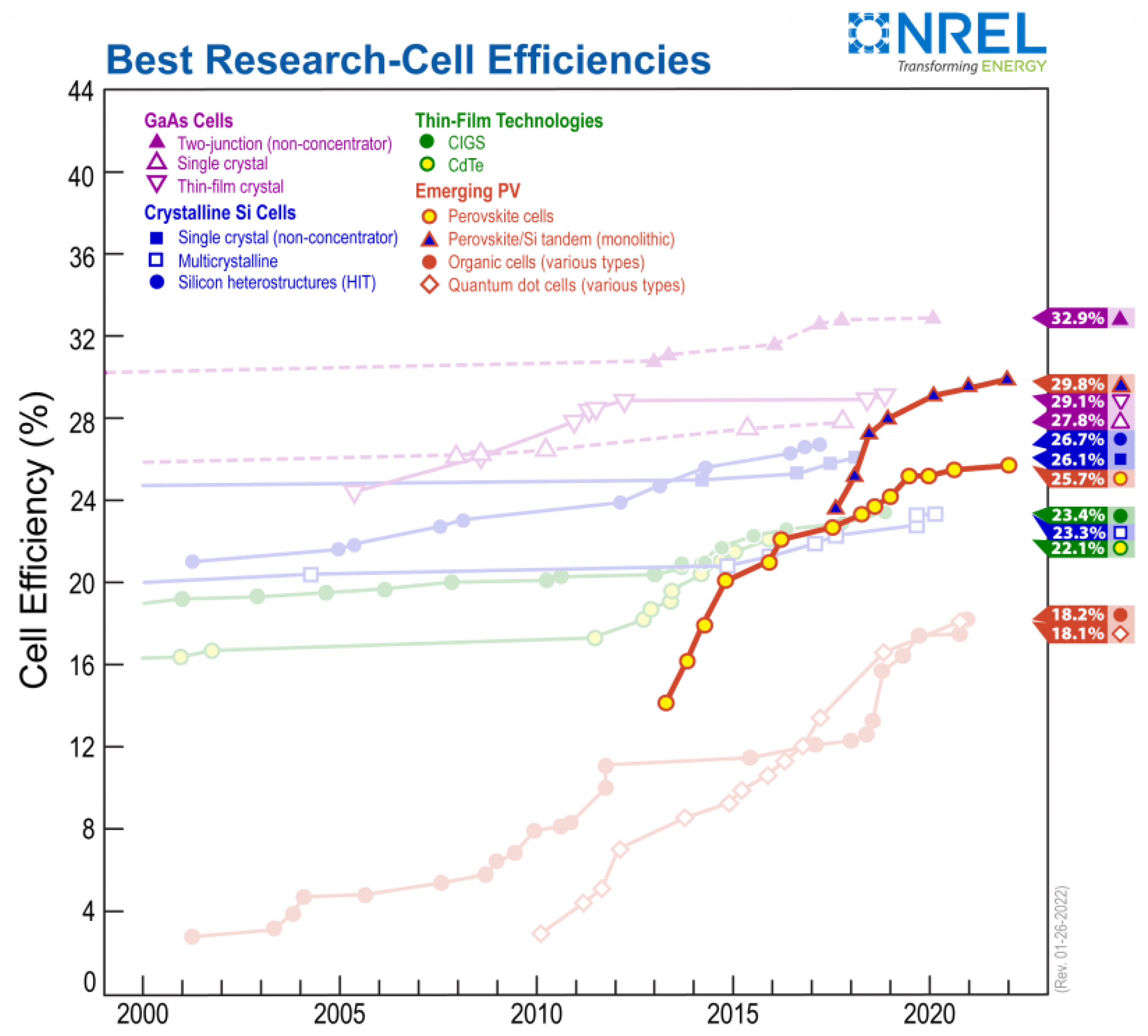
  121. NREL. Best Research-Cell Efficiences. 2022. Available online: https://www.nrel.gov/pv/cell-efficiency.html (accessed on 30 November 2022).
  122. Nandi, P.; Giri, C.; Swain, D. Room Temperature Growth of CH3NH3PbCl3 Single Crystals by Solvent Evaporation Method. CrystEngComm 2019, 21, 656–661. [Google Scholar] [CrossRef]
  123. Nandi, P.; Topwal, D.; Park, N.G.; Shin, H. Organic-Inorganic Hybrid Lead Halides as Absorbers in Perovskite Solar Cells: A Debate on Ferroelectricity. J. Phys. D Appl. Phys. 2020, 53, 493002. [Google Scholar] [CrossRef]
  124. Burschka, J.; Pellet, N.; Moon, S.J.; Humphry, R. Sequential Deposition as a Route to High-Performance Perovskite-Sensitized Solar Cells. Nature 2013, 499, 316–319. [Google Scholar] [CrossRef] [PubMed]
  125. Nandi, P.; Giri, C.; Bansode, U.; Topwal, D. CH3NH3PbI3 Based Solar Cell: Modified by Antisolvent Treatment. AIP Conf. Proc. 2017, 1832, 080065. [Google Scholar] [CrossRef]
  126. Nandi, P.; Giri, C.; Bansode, U.; Topwal, D. Study on CH3NH3PbI3 Based Perovskite Solar Cell: An Approach to Antisolvent Treatment under Ambient Condition. Recent Trends Chem. Mater. Sci. 2021, 3, 24–30. [Google Scholar] [CrossRef]
  127. Liu, D.; Kelly, T.L. Perovskite Solar Cells with a Planar Heterojunction Structure Prepared Using Room-Temperature Solution Processing Techniques. Nat. Photonics 2014, 8, 133–138. [Google Scholar] [CrossRef]
  128. Shi, J.; Dong, J.; Lv, S.; Xu, Y. Hole-Conductor-Free Perovskite Organic Lead Iodide Heterojunction Thin-Film Solar Cells: High Efficiency and Junction Property. Appl. Phys. Lett. 2014, 104, 63901. [Google Scholar] [CrossRef]
  129. Minemoto, T.; Murata, M. Impact of Work Function of Back Contact of Perovskite Solar Cells without Hole Transport Material Analyzed by Device Simulation. Curr. Appl. Phys. 2014, 14, 1428–1433. [Google Scholar] [CrossRef]
  130. Mohamad, N.; Arzaee, A.; Nawas, M.; Teridi, M. Superiority of Two-Step Deposition over One-Step Deposition for Perovskite Solar Cells Processed in High Humidity Atmosphere. Opt. Mater. 2021, 118, 111288. [Google Scholar] [CrossRef]
  131. Meng, L.; You, J.; Guo, T. Recent Advances in the Inverted Planar Structure of Perovskite Solar Cells. Acc. Chem. Res. 2016, 49, 155–165. [Google Scholar] [CrossRef]
  132. Park, N. Perovskite solar cells: An emerging photovoltaic technology. Mater. Today 2015, 18, 65–72. [Google Scholar] [CrossRef]
  133. Tablero, C. Absorption coefficients data of lead iodine perovskites using 14 different organic cations. Data Br. 2019, 27, 104636. [Google Scholar] [CrossRef]
  134. Zhang, P.; Li, M.; Chen, W. A Perspective on Perovskite Solar Cells: Emergence, Progress, and Commercialization. Front. Chem. 2022, 10, 802890. [Google Scholar] [CrossRef] [PubMed]
  135. Meng, L.; You, J.; Yang, Y. Addressing the stability issue of perovskite solar cells for commercial applications. Nat. Commun. 2018, 9, 5265. [Google Scholar] [CrossRef]
  136. Ball, J.; Petrozza, A. Defects in perovskite-halides and their effects in solar cells. Nat. Energy 2016, 1, 16149. [Google Scholar] [CrossRef]
  137. Askar, M.; Bernard, G.; Wiltshire, B. Multinuclear Magnetic Resonance Tracking of Hydro, Thermal, and Hydrothermal Decomposition of CH3NH3PbI3. J. Phys. Chem. C 2017, 121, 1013–1024. [Google Scholar] [CrossRef]
  138. Nandi, P.; Mahana, S.; Welter, E.; Topwal, D. Probing the Role of Local Structure in Driving the Stability of Halide Perovskites CH3NH3PbX3. J. Phys. Chem. C 2021, 125, 24655–24662. [Google Scholar] [CrossRef]
  139. Kim, Y.; Nandi, P.; Lee, D.; Shin, H. Stabilization of 3-D Trigonal Phase in Guanidinium (C(NH2)3) Lead Triiodide (GAPbI3) Films. Appl. Surf. Sci. 2021, 542, 148575. [Google Scholar] [CrossRef]
  140. Nandi, P.; Li, Z.; Kim, Y.; Ahn, T. Stabilizing Mixed Halide Lead Perovskites against Photoinduced Phase Segregation by A-Site Cation Alloying. ACS Energy Lett. 2021, 6, 837–847. [Google Scholar] [CrossRef]
  141. Nandi, P.; Giri, C.; Swain, D.; Manju, U. Temperature Dependent Photoinduced Reversible Phase Separation in Mixed-Halide Perovskite. ACS Appl. Energy Mater. 2018, 1, 3807–3814. [Google Scholar] [CrossRef]
  142. Jeong, S.; Seo, S.; Yang, H.; Park, H. Cyclohexylammonium-Based 2D/3D Perovskite Heterojunction with Funnel-Like Energy Band Alignment for Efficient Solar Cells (23.91%). Adv. Energy Mater. 2021, 11, 2102236. [Google Scholar] [CrossRef]
  143. Cao, J.; Yan, F. Recent Progress in Tin-Based Perovskite Solar Cells. Energy Environ. Sci. 2021, 14, 1286–1325. [Google Scholar] [CrossRef]
  144. Ahmad, U.; Kumar, S.; Hassan, A.; Mohsen, M. High power conversion efficiency of lead free perovskite solar cells: A theoretical investigation. Micromachines 2022, 13, 2201. [Google Scholar] [CrossRef]
  145. Nihal, G.; Salma, H.; Ahmed, S.; Fedawy, M. Design of lead free perovskite solar cell using Zn1-xMgxO as ETL: SCAPS device simulation. Optik 2021, 242, 167306. [Google Scholar] [CrossRef]
  146. Komal, K.; Abir, J.; Dey, A.; Subir, S. Lead free CH3NH3SnI3 based perovskite solar cell using ZnTe nano flowers as hole transport layer. Opt. Mater. 2021, 111, 110574. [Google Scholar] [CrossRef]
  147. Hadipour, A.; Boer, D.; Blom, P. Device operation of organic tandem solar cells. Org. Electron. 2008, 9, 617–624. [Google Scholar] [CrossRef]
  148. Grätzel, M. Dye-sensitized solar cells. J. Photochem. Photobiol. C Photochem. Rev. 2003, 4, 145–153. [Google Scholar] [CrossRef]
  149. Nazeeruddin, M.; Edgar, M.; Robin, H.; Nick, V. Redox regulation in ruthenium(II) polypyridyl complexes and their application in solar energy conversion. J. Chem. Soc. Dalton Trans. 1997, 23, 4571–4578. [Google Scholar] [CrossRef]
  150. Chiba, Y.; Islam, A.; Watanabe, Y.; Komiya, R. Dye-sensitized solar cells with conversion efficiency of 11.1%. Jpn. J. Appl. Phys. 2006, 45, L638. [Google Scholar] [CrossRef]
  151. Sarto, P.; Yukie, I. Clean and renewable energy from dye sensitized solar cells using fruit extracts. In Proceedings of the RIO 3—World Climate & Energy Event, Rio de Janeiro, Brazil, 1–5 December 2003; pp. 91–96. [Google Scholar]
  152. Lia, M.; Jojo, H.; Putri, N. Performance analysis of flexible DSSC with binder addition. AIP Conf. Proc. 2016, 1725, 020050. [Google Scholar] [CrossRef] [Green Version]
  153. Hardani, H.; Ridwan, H.; Suhada, A. Ruthenium (N719) Optimization to Improve Dye Sensitized Solar Cell Efficiency. Int. J. Thin Film Sci. Technol. 2022, 11, 47–53. [Google Scholar]
  154. Hardani, I.S.; Mustariani, B.; Dewi, Y.K. Efficient TiO2 nanoparticle-ruthenium sensitizers with high open-circuit voltage (Voc) for high-performance dye-sensitized solar cells. J. Phys. Conf. Ser. 2021, 1816, 012005. [Google Scholar] [CrossRef]
  155. Gao, F.; Bard, A.; Kispert, L. Photocurrent generated on a carotenoid-sensitized TiO2 nanocrystalline mesoporous electrode. J. Photochem. Photobiol. A Chem. 2000, 130, 49–56. [Google Scholar] [CrossRef]
  156. Kalyanasundaram, K.; Gratzel, M. Applications of functionalized transition metal complexes in photonic and optoelectronic devices. Coord. Chem. Rev. 1998, 177, 347–414. [Google Scholar] [CrossRef]
  157. Hardani, H.; Alpiana, H.; Lily, M. Making prototype dye sensitized solar cells (DSSC) based on TiO2 nanopory using extration of mangsteen peel (Garnicia mangostana). Indones. Phys. Rev. 2018, 1, 55–65. [Google Scholar] [CrossRef]
  158. Qadir, M.; Sun, K.; Sahito, I.; Arbab, A. Composite multi-functional over layer: A novel design to improve the photovoltaic performance of DSSC. Sol. Energy Mater. Sol. Cells 2015, 140, 141–149. [Google Scholar] [CrossRef]
  159. Wang, S.; Ding, Z.; Chang, X.; Xu, J. Modified Nano-TiO2 Based Composites for Environmental Photocatalytic Applications. Catalysts 2020, 10, 759. [Google Scholar] [CrossRef]
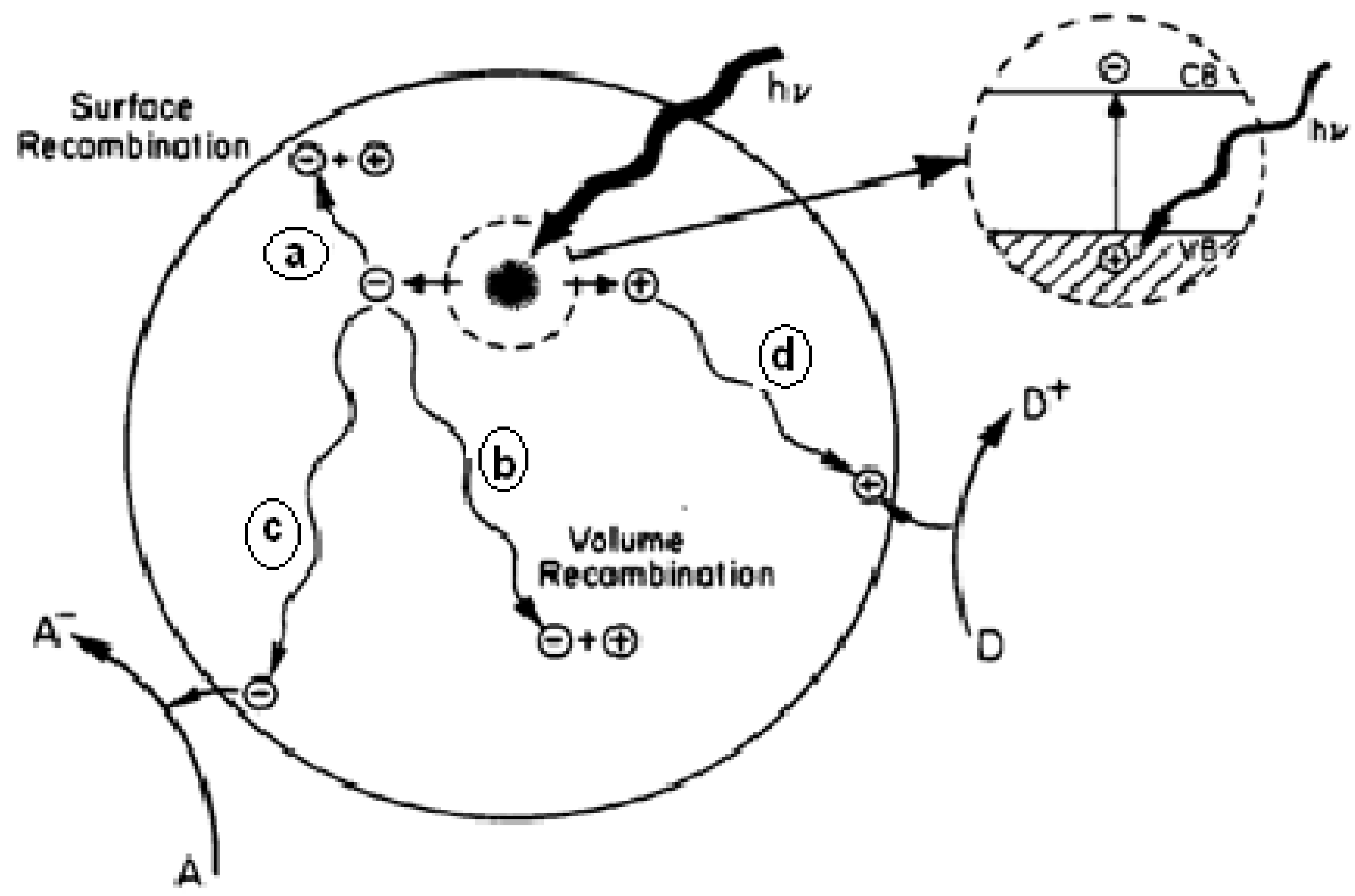
  160. Linsebigler, A.; Lu, G.; Yates, J.T. Photocatalysis on TiO2 Surfaces: Principles, Mechanisms, and Selected Results. Chem. Rev. 1995, 95, 735–758. [Google Scholar] [CrossRef]
  161. Berger, T.; Sterrer, M.; Diwald, O.; Knözinger, E.; Panayotov, D. Light-induced charge separation in anatase TiO2 particles. J. Phys. Chem. B 2005, 109, 6061–6068. [Google Scholar] [CrossRef]
  162. Darmawan, M.; Zaidah, A.; Hidayatulloh, A.; Mentari, I. Performance of Cosmos caudatus chlorophyll dye on TiO2 nano particles coating in the manufacture of Dye-Sensitized Solar Cells (DSSC). J. Phys. Conf. Ser. 2021, 1869, 012108. [Google Scholar] [CrossRef]
  163. Liu, J.; Zhou, H.; Song, L.; Yang, Z.; Qiu, M. Anthocyanins: Promising Natural Products with Diverse Pharmacological Activities. Molecules 2021, 26, 3807. [Google Scholar] [CrossRef]
  164. Oluwaseun, A.; Mojoyinola, K.; Lydia, A.; Bello, T. Fruit peels pigment extracts as a photo sensitizer in ZnO based dye sensitized solar cells. Chem. Phys. Impact. 2021, 3, 100039. [Google Scholar] [CrossRef]
  165. Cuttriss, A.; Cazzonelli, C.; Wurtzel, E.; Pogson, B. Carotenoids. Adv. Bot. Res. 2011, 58, 1–36. [Google Scholar]
  166. Sims, D.; Gamon, J. Relationships between leaf pigment content and spectral reflectance across a wide range of species, leaf structures and developmental stages. Remote Sens. Environ. 2003, 81, 337–354. [Google Scholar] [CrossRef]
  167. Song, H.; Luo, S.; Huang, H.; Deng, B. Solar-Driven Hydrogen Production: Recent Advances, Challenges, and Future Perspectives. ACS Energy Lett. 2022, 7, 1043–1065. [Google Scholar] [CrossRef]
  168. Sharma, K.; Sharma, V.; Sharma, S. Dye-Sensitized Solar Cells: Fundamentals and Current Status. Nanoscale Res. Lett. 2018, 13, 381. [Google Scholar] [CrossRef] [PubMed]
  169. Altobello, S.; Bignozzi, A.; Giovanni, M.; Rajae, L. Sensitization of TiO2 with ruthenium complexes containing boronic acid functions. J. Photochem. Photobiol. A Chem. 2004, 166, 91–98. [Google Scholar] [CrossRef]
  170. Weidenspointner, G.; Andritschke, R.; Aschauer, S.; Erdinger, F.; Fischer, P. Calibration of the non-linear system response of a prototype set-up of the DSSC detector for the European XFEL. In Proceedings of the IEEE Nuclear Science Symposium Conference Record, Anaheim, CA, USA, 27 October–3 November 2012. [Google Scholar] [CrossRef]
  171. Ho, S.M.; Hardani, A.S. Thin film based solar cell and dye sensitized solar cells: Review. Int. J. Adv. Sci. Technol. 2020, 29, 2413–2426. [Google Scholar]
  172. Halme, J. Dye-Sensitized Nanostructured and Organic Photovoltaic Cells: Technical Review and Preliminary Tests; Department of Engineering, Physics and Mathematics, Helsinki University of Technology: Helsinki, Finland, 2022. [Google Scholar]
  173. Gupta, D.; Vishnu, C.; Kumar, R. Sputter deposition of 2D MoS2 thin films—A critical review from a surface and structural perspective. Inorg. Chem. Commun. 2022, 144, 109848. [Google Scholar] [CrossRef]
  174. Xavier, M.; Pantoja, E.; Romeo, A.; Tiwari, A. CdTe/CdS solar cells on flexible substrates. Sol. Energy 2004, 77, 831–838. [Google Scholar]
  175. Fulop, G.; Doty, M.; Betz, J.; Liu, H. High-efficiency electrodeposited cadmium telluride solar cells. Appl. Phys. Lett. 1982, 40, 327. [Google Scholar] [CrossRef]
  176. Lepiller, C.; Cowache, P.; Gibson, N.; Ozsan, E.; Lincot, D. Fast electrodeposition route for cadmium telluride solar cells. Thin Solid Films 2000, 361–362, 118–122. [Google Scholar] [CrossRef]
  177. Qian, L.; Fu, W.; Chi, K.; Yang, L.; Lv, P.; Zhou, L. Effects of CTAB concentrations on properties of electrodeposited cadmium telluride films. CrystEngComm 2014, 16, 5227–5233. [Google Scholar]
  178. Suha, A.; Hamid, M.; Hussein, A.; Shihab, A. Enhanced efficiency of CdTe photovoltaic by thermal evaporation vacuum. Energy Proc. 2019, 157, 635–643. [Google Scholar]
  179. Amit, M.; Jason, M.; Ali, A.; Sampath, S.; John, M. Polycrystalline CdTe photovoltaics with efficiency over 18% through improved absorber passivation and current collection. Sol. Energy Mater. Sol. Cells 2018, 176, 9–18. [Google Scholar]
  180. Dipendra, A.; Junda, M.; Ebin, B.; Randall, J.; Nikolas, P. Glancing angle deposited CdTe: Nanostructured films and impact on solar cell performance. Surf. Coat. Technol. 2020, 381, 125127. [Google Scholar] [CrossRef]
  181. Ebin, B.; Fadhil, K.; Adam, B.; Heben, J.; Randy, J. Wet chemical etching of cadmium telluride photovoltaics for enhanced open-circuit voltage, fill factor, and power conversion efficiency. J. Mater. Res. 2019, 34, 3988–3997. [Google Scholar] [CrossRef]
  182. Kamala, K.; Ebin, B.; Indra, S.; Suman, R.; Manoj, K.; Heben, J. Semi-Transparent p-Type Barium Copper Sulfide as a Back Contact Interface Layer for Cadmium Telluride Solar Cells. Sol. Energy Mater. Sol. Cells 2020, 218, 110764. [Google Scholar] [CrossRef]
  183. Gupta, A.; Viral, P.; Alvin, D. High efficiency ultra-thin sputtered CdTe solar cells. Sol. Energy Mater. Sol. Cells 2006, 90, 2263–2271. [Google Scholar] [CrossRef]
  184. Akhlesh, G.; Alvin, D. All-sputtered 14% CdS∕CdTe thin-film solar cell with ZnO:Al transparent conducting oxide. Appl. Phys. Lett. 2004, 85, 684. [Google Scholar] [CrossRef]
  185. Susumu, K.; Ezumi, H. Preparation of CdS/CdTe solar cell by laser ablasion. Sol. Energy Mater. Sol. Cells 1994, 35, 299–303. [Google Scholar]
  186. Chao, D.; Ming, Z.; Li, B.; Feng, L.; Wu, J. Preparation and characterization of pulsed laser deposited CdTe thin films at higher FTO substrate temperature and in Ar + O2 atmosphere. Mater. Sci. Eng. B 2013, 178, 801–806. [Google Scholar]
  187. Min, S.; Jo, J.; Cho, A.; Yun, H.; Kim, K.; Ahn, S. Semi-transparent photovoltaics using ultra-thin Cu(In,Ga)Se2 absorber layers prepared by single-stage co-evaporation. Sol. Energy 2019, 181, 276–284. [Google Scholar]
  188. Yen, Y.; Lin, Y.; Chang, S.; Hong, H.; Tuan, H.; Chueh, Y. Investigation of bulk hybrid heterojunction solar cells based on Cu(In,Ga)Se2 nanocrystals. Nanoscale Res. Lett. 2013, 8, 329. [Google Scholar] [CrossRef] [PubMed]
  189. Jheng, B.; Liu, P.; Wu, M. Efficiency enhancement of non-selenized Cu(In,Ga)Se2 solar cells employing scalable low-cost antireflective coating. Nanoscale Res. Lett. 2014, 9, 331. [Google Scholar] [CrossRef] [PubMed]
  190. Chirila, A.; Fabian, P.; Stephan, B.; Uhl, R.; Verma, R.; Shiro, N.; Lukas, K. Highly efficient Cu(In,Ga)Se2 solar cells grown on flexible polymer films. Nat. Mater. 2011, 10, 857–861. [Google Scholar] [CrossRef]
  191. Sim, J.; Kang, S.; Nandi, R.; Jeong, K.; Lee, C. Implementation of graphene as hole transport electrode in flexible CIGS solar cells fabricated on Cu foil. Sol. Energy 2018, 162, 357–363. [Google Scholar] [CrossRef]
  192. Mitzi, B.; Yuan, M.; Jay, S.; Alex, G. Hydrazine-based deposition route for device-quality CIGS films. Thin Solid Films 2009, 517, 2158–2162. [Google Scholar] [CrossRef]
  193. Binetti, S.; Mereu, R.; Donne, A.; Meschia, M.; Garattini, P. Fabricating Cu(In,Ga)Se2 solar cells on flexible substrates by a new roll-to-roll deposition system suitable for industrial applications. Semicond. Sci. Technol. 2015, 30, 105006. [Google Scholar] [CrossRef]
  194. Bloesch, P.; Uhl, A.; Tiwari, A.; Bilger, G.; Verma, R. Cu(In,Ga)Se2 solar cell grown on flexible polymer substrate with efficiency exceeding 17%. Prog. Photovolt. 2011, 19, 560–564. [Google Scholar]
  195. Fraga, D.; Carda, J.; Calvet, I.; Barrachina, E. Developing CIGS solar cells on glass-ceramic substrates. Mater. Lett. 2018, 221, 104–106. [Google Scholar] [CrossRef]
  196. Wei, W.; Su, Y.; Chang, C. Inkjet printed chalcopyrite CuInxGa1−xSe2 thin film solar cells. Sol. Energy Mater. Sol. Cells 2011, 95, 2616–2620. [Google Scholar]
  197. Xu, C.; Zhang, H.; Parry, J.; Perera, S.; Zeng, H. A single source three-stage evaporation approach to CIGS absorber layer for thin film solar cells. Sol. Energy Mater Sol. Cells 2013, 117, 357–362. [Google Scholar] [CrossRef]
  198. Raghu, N.; Arturo, M. CuIn1−xGaxSe2-based photovoltaic cells from electrodeposited precursor films. Sol. Energy Mater. Sol. Cells 2003, 76, 331–337. [Google Scholar]
  199. Bhattacharya, N.; Hiltner, F.; Noufi, N.; Sites, R.; Batchelor, W. 15.4% CuIn1-xGaxSe2 based photovoltaic cells from solution based precursor films. Presented at the European Materials Research Society Meeting, Strasbourg, France, 1–4 June 1999. NREL/CP-590-26611. [Google Scholar]
  200. Zank, J.; Mehlin, M.; Fritz, P. Electrochemical co-deposition of indium and gallium for chalcopyrite solar cells. Thin Solid Films 1996, 286, 259–263. [Google Scholar] [CrossRef]
  201. Guimard, D.; Kurdi, J.; Lincot, D.; Grand, P.; Bodereau, N. Efficient CIGS solar cells prepared by electrodeposition. In Proceedings of the 3rd World Conference on Photovoltaic Energy Conversion, Osaka, Japan, 11–18 May 2003. [Google Scholar]
  202. Ganchev, M.; Kois, J.; Kaelin, M.; Tiwari, A. Preparation of Cu(In,Ga)Se2 layers by selenization of electrodeposited Cu–In–Ga precursors. Thin Solid Films 2006, 511–512, 325–327. [Google Scholar] [CrossRef]
  203. Dale, P.; Anura, P.; Zoppt, G.; Ian, F.; Scilla, R. Deposition and Characterization of Copper Chalcopyrite Based Solar Cells using Electrochemical Techniques. ECS Meet. Abstr. 2007, 6, 535. [Google Scholar] [CrossRef]
  204. Feng, K.; Ao, J.; Sun, G.; He, Q.; Sun, Y. Properties of CuInxGa1−xSe2 thin films grown from electrodeposited precursors with different levels of selenium content. Curr. Appl. Phys. 2010, 10, 886–888. [Google Scholar]
  205. Hilda, R.; Hasan, T.; Siti, Z.; Nandang, M. Electrodeposition Technique to Fabrication CIGS using Pure Selenium and SeO2 as Selenium Source. Mal. J. Fund. Appl. Sci. 2022, 18, 367–373. [Google Scholar]
  206. Chen, S.; Wang, S.; Kuo, S.; Juang, J.; Lee, P. A Comprehensive Study of One-Step Selenization Process for Cu(In1−xGax)Se2 Thin Film Solar Cells. Nanoscale Res. Lett. 2017, 12, 208. [Google Scholar] [CrossRef]
  207. Song, X.; Xu, J.; Li, M.; Lin, W.; Luo, X. A review on development prospect of CZTS based thin film solar cells. Int. J. Photoenergy 2014, 2014, 613173. [Google Scholar] [CrossRef]
  208. Nandur, A.; White, B. Growth of Cu2ZnSnS4 (CZTS) by Pulsed Laser Deposition for Thin Film Photovoltaic Absorber Material. In Proceedings of the APS March Meeting 2014, Denver, CO, USA, 3–7 March 2014; Available online: https://ui.adsabs.harvard.edu/abs/2014APS..MARF24003N/abstract (accessed on 30 November 2022).
  209. Tiwari, D.; Tapas, K.; Ray, A.; Dutt, T. Cu2ZnSnS4 thin films by simple replacement reaction route for solar photovoltaic application. Thin Solid Films 2014, 551, 42–45. [Google Scholar] [CrossRef]
  210. Wei, W.; Shen, H.; Yao, H.; Tang, Z.; Lu, Y. Effect of sulfurization temperature on the property of Cu2ZnSnS4 thin film by eco-friendly nanoparticle ink method. Appl. Phys. A 2017, 123, 599. [Google Scholar] [CrossRef]
  211. Ennaoui, A.; Hock, R.; Jost, S.; Kirbs, A.; Weber, A.; Lux, M. Cu2ZnSnS4 thin film solar cells from electroplated precursors: Novel low-cost perspective. Thin Solid Films 2009, 517, 2511–2514. [Google Scholar] [CrossRef]
  212. Tsai, H.; Chen, Y.; Wang, Y.; Chen, C.; Thomas, R.; Hsu, C.; Chueh, Y. Facile Growth of Cu2ZnSnS4Thin-Film by One-Step Pulsed Hybrid Electrophoretic and Electroplating Deposition. Sci. Rep. 2016, 6, 19102. [Google Scholar] [CrossRef] [PubMed]
  213. Li, Z.; Wang, S.; Ma, X.; Min, Y.; Liu, T.; Liu, S. A simple structure of Cu2ZnSnS4/CdS solar cells prepared by sputtering. Phys. B Condens. Matter 2017, 526, 80–83. [Google Scholar] [CrossRef]
  214. Sandip, M.; Ramphal, S.; Dimitra, S.; Elias, S.; Huse, N. Enhancement in the efficiency of crystalline Cu2ZnSnS4 thin film solar cell by using various buffer layers. Superlattices Microstruct. 2017, 109, 240–248. [Google Scholar]
  215. Scragg, J.; Tomas, K.; Timo, W.; Tove, E.; Margareta, K. Effects of Back Contact Instability on Cu2ZnSnS4 Devices and Processes. Chem. Mater. 2013, 25, 3162–3171. [Google Scholar] [CrossRef]
  216. Khalil, M.; Nobili, L.; Magagnin, L.; Donne, A.; Mereu, A.; Hart, L. CZTS thin flm solar cells on fexible Molybdenum foil by electrodeposition-annealing route. J. Appl. Electrochem. 2021, 51, 209–218. [Google Scholar] [CrossRef]
  217. Rongrong, C.; Fan, J.; Li, H.; Liu, C.; Mai, Y. Efficiency enhancement of Cu2ZnSnS4 solar cells via surface treatment engineering. R. Soc. Open Sci. 2018, 5, 171163. [Google Scholar] [CrossRef]
  218. Jian, C.; Yan, C.; Wei, L.; Ning, S.; Liu, F.; Huang, S. Cu2ZnSnS4 thin film solar cell fabricated by magnetron sputtering and sulfurization. MRS Online Proc. Libr. 2014, 1638, 901. [Google Scholar] [CrossRef]
  219. Cho, J.; Agus, I.; Park, S.; Kim, W.; Yoon, S.; Min, K. Synthesis of Cu2ZnSnS4 Thin Films by a Precursor Solution Paste forThin Film Solar Cell Applications. ACS Appl. Mater. Interfaces 2013, 5, 4162–4165. [Google Scholar] [CrossRef]
  220. Vigil, O.; Maykel, C.; Jimenez, D.; Aguilar, M. Electrical properties of sprayed Cu2ZnSnS4 thin films and its relation with secondary phase formation and solar cell performance. Sol. Energy Mater. Sol. Cells 2015, 132, 557–562. [Google Scholar] [CrossRef]
  221. Yusuf, Y.; Eka, C.; Gema, R.; Harbi, S.; Harito, C. All-Solution-Non-Vacuum Fabrication Process of CZTS Solar Cell using ZTO as Non-Toxic Buffer Layer. Int. J. Nanoelectron. Mater. 2020, 13, 307–314. [Google Scholar]
  222. Hu, J.; Tong, W.; Muhammad, I.; Umar, F.; Shuo, C. Pulsed laser deposited and sulfurized Cu2ZnSnS4 thin film for efficient solar cell. Sol. Energy Mater. Sol. Cells 2021, 233, 111383. [Google Scholar] [CrossRef]
  223. Tatsuo, F.; Hiroshi, N.; Shin, T.; Ito, T.; Ryoji, A. Fabrication of Cu2ZnSnS4 thin film solar cells by sulfurization. R&D Rev. Toyota CRDL 2013, 44, 1–18. [Google Scholar]
  224. Hyun, Y.; Ji, H.; Joshi, B.; Ra, Y.; Sam, Y.; Ho, K.; Scott, J. CuInSe2 (CIS) Thin Film Solar Cells by Electrostatic Spray Deposition. J. Electrochem. Soc. 2012, 159, H444–H449. [Google Scholar]
  225. Vahid, A.; Brian, W.; Matthew, G.; Reid, K. Spray-deposited CuInSe2 nanocrystal photovoltaics. Energy Environ. Sci. 2010, 3, 1600–1606. [Google Scholar]
  226. Meadows, H.; Regesch, D.; Sendler, J.; Misra, S.; Gerliz, V.; Dale, P. CuInSe2 semiconductor formation by laser annealing. Thin Solid Films 2015, 582, 23–26. [Google Scholar] [CrossRef]
  227. Sejin, A.; Tae, H.; Ara, C.; Jae, H.; Shin, K.; Yoon, K.; Park, H. CuInSe2 Thin-Film Solar Cells with 7.72% Efficiency Prepared via Direct Coating of a Metal Salts/Alcohol-Based Precursor Solution. ChemSusChem 2012, 5, 1773–1777. [Google Scholar]
  228. Ara, C.; Ahn, S.; Yoon, H.; Gwak, J.; Ahn, K.; Shin, K. Non-vacuum processed CuInSe2 thin films fabricated with a hybrid ink. Sol. Energy Mater. Sol. Cells 2013, 109, 17–25. [Google Scholar]
  229. Saidi, H.; Durand, B.; Lazzari, J.; Boujmil, M. Elaboration and characterization of CuInSe2 thin films using one step electrodeposition method on silicon substrate for photovoltaic application. Mater. Res. Express 2018, 5, 016414. [Google Scholar] [CrossRef]
  230. Mandati, S.; Misra, P.; Boosagulla, D. Economic pulse electrodeposition for flexible CuInSe2 solar cells. Mater. Renew Sustain. Energy 2020, 9, 19. [Google Scholar] [CrossRef]
  231. Kar, M.; Hugh, W.; Hugh, H. Chemical liquid deposition of CuInSe2 and CuIn(S,Se)2 films for solar cells. Thin Solid Films 2012, 520, 5431–5437. [Google Scholar] [CrossRef]
  232. Se, A.; Kim, C.; Yun, H.; Gwak, J.; Jeong, S.; Ryu, B. CuInSe2 (CIS) Thin Film Solar Cells by Direct Coating and Selenization of Solution Precursors. J. Phys. Chem. C 2010, 114, 8108–8113. [Google Scholar]
  233. Huang, W.; Lyu, L.; Huang, M.; Chang, S.; Tseng, C.; Tuan, H. Solvothermal Synthesis of Zincblende and Wurtzite CuInS2 Nanocrystals and Their Photovoltaic Application. Langmuir 2012, 28, 8496–8501. [Google Scholar] [CrossRef] [PubMed]
  234. Wangwei, C.; Qi, J.; Dong, C.; Chen, J.; Shen, Z.; He, Y.; Yang, S. Solution-Processed in Situ Growth of CuInS2 Nanoparticle Films for Efficient Planar Heterojunction Solar Cells with a Dual Nature of Charge Generation. ACS Appl. Energy Mater. 2019, 2, 5231–5242. [Google Scholar]
  235. Scheer, R.; Walter, T.; Schock, W.; Lewerenz, H. CuInS2 based thin film solar cells with 10.2% efficiency. Appl. Phys. Lett. 1993, 63, 3294. [Google Scholar] [CrossRef]
  236. Weil, B.; Yi, C.; Connor, T. CuInS2 Solar Cells by Air-Stable Ink Rolling. J. Am. Chem. Soc. 2010, 132, 6642–6643. [Google Scholar] [CrossRef]
  237. Mehdi, D.; Ershad, P.; Tehrani, A.; Nima, T. A novel low-temperature growth of uniform CuInS2 thin films and their application in selenization/sulfurization-free CuInS2 solar cells. Mater. Today Commun. 2021, 26, 102050. [Google Scholar] [CrossRef]
  238. Hina, P.; Khan, S.; Ahmed, N.; Jamil, Q. Synthesis and characterization of CuInS2 nanostructures and their role in solar cell applications. Mater. Chem. Phys. 2022, 290, 126602. [Google Scholar] [CrossRef]
  239. Woo, J.; Park, S.; Kim, W.; Kim, M. Fabrication of nanocrystal ink-based superstrate-type CuInS2 thin film solar cells. Nanotechnology 2012, 23, 265401. [Google Scholar] [CrossRef]
  240. Tang, M.; Tian, Q.; Hu, X.; Peng, Y.; Xue, Y.; Yang, J.; Hu, J. In situ preparation of CuInS2 films on a flexible copper foil and their application in thin film solar cells. CrystEngComm 2012, 14, 1825–1832. [Google Scholar] [CrossRef]
  241. Lakhe, M.; Nandu, B. Characterization of electrochemically deposited CuInTe2 thin films for solar cell applications. Sol. Energy Mater. Sol. Cells 2014, 123, 122–129. [Google Scholar] [CrossRef]
  242. Manorama, L.; Nandu, B.; Mahapatra, S. Development of CuInTe2 thin film solar cells by electrochemical route with low temperature (80 °C) heat treatment procedure. Mater. Sci. Eng. B 2016, 204, 20–26. [Google Scholar]
  243. Jing, G.; Pei, Y.; Zhou, Z.; Zhou, W.; Kou, D.; Wu, S. Solution-Processed Cu2ZnSn(S,Se)4 Thin-Film Solar Cells Using Elemental Cu, Zn, Sn, S, and Se Powders as Source. Nanoscale Res. Lett. 2015, 10, 335. [Google Scholar] [CrossRef]
  244. Gee, Y.; Ju, R.; Jo, W.; Son, D.; Kim, D.; Kang, J. Nanoscale observation of surface potential and carrier transport in Cu2ZnSn(S,Se)4 thin films grown by sputtering-based two-step process. Nanoscale Res. Lett. 2014, 9, 10. [Google Scholar] [CrossRef]
  245. Chate, P.; Hankare, P.; Sathe, D. Characterization of cadmium selenide films for photovoltaic applications. J. Alloys Compd. 2010, 505, 140–143. [Google Scholar] [CrossRef]
  246. Kanghua, L.; Lin, X.; Song, B.; Yang, X.; Chen, C.; Tang, J. Rapid thermal evaporation for cadmium selenide thin-film solar cells. Front. Optoelectron. 2021, 14, 482–490. [Google Scholar]
  247. Wang, K.; Cheng, J.; Yang, X. Enhanced Photovoltaic Properties in Sb2S3 Planar Heterojunction Solar Cell with a Fast Selenylation Approach. Nanoscale Res. Lett. 2018, 13, 270. [Google Scholar] [CrossRef]
  248. Hsiao, Y.; Lu, C.; Ji, L. Characterization of photovoltaics with In2S3 nanoflakes/p-Si heterojunction. Nanoscale Res. Lett. 2014, 9, 32. [Google Scholar] [CrossRef]
  249. Mostafa, S.; Atef, S.; Ahmed, I.; Said, E. Synthesis, Characterization and Performance of Cu2SnS3 for Solar Cell Application. Int. J. Sci. Eng. Res. 2015, 6, 1447–1453. [Google Scholar]
  250. Chaudhari, J.; Joshi, U. Fabrication of high quality Cu2SnS3 thin film solar cell with 1.12% power conversion efficiency obtain by low cost environment friendly sol-gel technique. Mater. Res. Express 2018, 5, 036203. [Google Scholar] [CrossRef]
  251. Prasert, S.; Katy, H.; Kim, S.; Heo, J.; Helen, H.; Tonio, B. Enhancing the efficiency of SnS solar cells bia band off set engineering with a zinc oxysulfide buffer layer. Appl. Phys. Lett. 2013, 110, 10539. [Google Scholar] [CrossRef]
  252. Vinaya, K.; Shin, Y.; Kim, J. Photovoltaic behavior of the room temperature grown RF-Sputtered SnS thin films. Opt. Mater. 2019, 88, 594–600. [Google Scholar]
  253. Tien, D.; Van, T.; Manh, H.; Kumar, V.; Raj, M. Synthesis of Ag-embedded SnS films by the RF method for photovoltaic applications. Surf. Interfaces 2021, 25, 101151. [Google Scholar] [CrossRef]
  254. Joel, V.; Joao, O.; Jacek, J.; Della, E.; Chesman, S. Solution-Processed CuSbS2 Thin Films and Superstrate Solar Cells with CdS/In2S3 Buffer Layers. ACS Appl. Energy Mater. 2020, 3, 7885–7895. [Google Scholar]
  255. Qinmiao, C.; Dou, X.; Li, Z.; Chen, J.; Zhou, F.; Zhuang, S. Study on the photovoltaic property of Cu4SnS4 synthesized by mechanochemical process. Optik 2014, 125, 3217–3220. [Google Scholar]
  256. Mohsen, C.; Farid, J.; Ramin, Y. Optical, electrical, and photovoltaic properties of PbS thin films by anionic and cationic dopants. Appl. Phys. A Mater. Sci. Process. 2017, 123, 390. [Google Scholar] [CrossRef]
  257. Rex, S.; Deva, A.; Shkir, M.; AlFaify, S.; Valanarasu, S. Fabrication and characterization of lead sulfide (PbS) thin film based heterostructure (FTO/CdS/PbS/Ag) solar cell by nebulizer spray method. Mater. Res. Express 2019, 6, 056416. [Google Scholar] [CrossRef]
  258. Ho, S.M. Studies of Power Conversion Efficiency and Optical Properties of Ni3Pb2S2 Thin Films. Makara J. Sci. 2017, 21, 3. [Google Scholar] [CrossRef]
  259. Kisan, C.; Guar, L.; Pradip, D.; Sanadi, R.; Kamble, G. Photovoltaic Application Study of Zinc Telluride Thin Films Grown by Chemical Bath Deposition Method. Adv. Mater. Phys. Chem. 2021, 11, 131–144. [Google Scholar]
  260. Thambidurai, M.; Lee, C.; Dhayalan, V.; Muthukumarasamy, N. Quantum confinement effects in Gd-doped CdS nanoparticles prepared by chemical precipitation technique. J. Mater. Sci. Mater. Electron. 2013, 24, 4535–4541. [Google Scholar] [CrossRef]
  261. Baskoutas, S.; Poulopoulos, P.; Karoutsos, V.; Flevaris, K. Strong quantum confinement effects in thin zinc selenide films. Chem. Phys. Lett. 2006, 417, 461–464. [Google Scholar] [CrossRef]
  262. Azizian, K.; Zeng, Z.; Khodayari, Y. Strong quantum confinement effects in SnS nanocrystals produced by ultrasound assisted method. J. Nanopart. Res. 2013, 15, 1388. [Google Scholar] [CrossRef]
  263. Keyur, S.; Patel, K.; Solamki, G. Structural and optical characterization of nanocrystalline SnSe thin film. Int. J. Res. Innov. Appl. Sci. 2016, 1, 6–11. [Google Scholar]
  264. Ogherohwo, E.; Barnabas, B.; Alafiatayo, A. Investigating the wavelength of light and its effects on the performance of a solar photovoltaic module. Int. J. Innov. Res. Comput. Sci. Technol. 2015, 3, 61–64. [Google Scholar]
  265. Available online: https://www.alliedmarketresearch.com/thin-film-solar-cell-market (accessed on 28 December 2022).
Figure 1. The structures of some important donor and acceptor materials of OSC.
Applsci 13 02051 g001
Figure 2. The fabrication of OSC: (A) single active layer, (B) bilayer heterojunction, (C) bulk heterojunction, (D) tandem heterojunction.
Applsci 13 02051 g002
Figure 3. Energy level diagram demonstrating the operation of OSC.
Applsci 13 02051 g003
Figure 4. Current voltage (IV) curve of organic solar cells.
Applsci 13 02051 g004
Figure 5. (a) 3D and (b) 2D schematic diagrams and (c) the schematic diagram of a perovskite unit cell [116].
Applsci 13 02051 g005
Figure 6. The efficiency records for perovskite solar cells and monolithic perovskite/Si tandem solar cells compared with other photovoltaic technologies [121].
Applsci 13 02051 g006
Figure 7. The effect of the perovskite layer thickness on solar cell parameters [144].
Applsci 13 02051 g007
Figure 8. Changes in the particle size of anatase and rutile as a function of annealing temperature [158].
Applsci 13 02051 g008
Figure 9. The schematic of photoexcitation followed by de-excitation on the semiconductor’s surface [160].
Applsci 13 02051 g009
Figure 10. The structure of beta-carotene [169].
Applsci 13 02051 g010
Figure 11. The working principle of dye-sensitized solar cells [172].
Applsci 13 02051 g011
Figure 12. Crystal structures of (a) stannite and (b) kesterite [207].
Applsci 13 02051 g012
Table 1. Trivial name and semi-systematic names of carotenoids.
Trivial NameSemi-Systematic Name
ζ -carotene7,8,7′,8′-tetrahydro- ψ , ψ -carotene
Neurosporene7,8-dihydro- ψ , ψ -carotene
Pro-lycopene7Z,9Z,7′Z,9′Z-tetra-cis- ψ , ψ -carotene
Lycopene ψ , ψ -carotene
γ -carotene β , ψ -carotene
δ -carotene ε , ψ -carotene
α -carotene β , ε -carotene
zeinoxanthin β , ε -carotene-3,-ol
lutein β , ε -carotene-3,3′-diol
β -carotene7,8-dihydro- β ,   β -carotene
β -cryptoxanthin β ,   β -carotene-3-ol
Zeaxanthin β ,   β -carotene-3,3′-diol
antheraxanthin5,6-epoxy-5,6-dihydro- β , β -carotene-3,3′-diol
Table 2. The growth of CdTe films using various deposition methods and the photovoltaic properties.
Deposition TechniquePhotovoltaic PropertiesReference
Voc (mV)Isc (mA/cm2)PEC (%)FF (%)
Electro deposition72318.78.664[175]
Electro deposition70018.16-[176]
Electro deposition250–2904.12–6.350.28–0.9225–52[177]
Thermal-evaporation method51918.196.445.6[178]
Evaporation method86327.118.780.5[179]
Glancing angle-deposition method774231161.9[180]
Vapor-transport deposition806–83920.2–21.612.5–13.573.3–76.9[181]
Vapor-transport deposition683–83922.2–22.99.2–14.460.6–75[182]
Sputtering method--11.2-[183]
Radio-frequency sputtering--14-[184]
Laser-ablation method60013340[185]
Pulsed-laser deposition--6.68-[186]
Table 3. The growth of CIGS films using various deposition methods and the photovoltaic properties.
Deposition TechniquePhotovoltaic PropertiesReference
Voc (mV)Isc (mA/cm2)PEC (%)FF (%)
Co-evaporation method--6.46–9.78-[187]
chemical bath deposition method7600.0590.01125.1[188]
Co-sputtering method551–55322.7–29.59.1–11.168.4–72.3[189]
Vacuum evaporation method71234.818.775.7[190]
Chemical vapor deposition--9.9164.75[191]
Spin-coating method--10-[192]
Sputtering and evaporation method--20.4-[193]
Vacuum evaporation--17.1-[194]
Co-precipitation method168.28.110.427.6[195]
Inkjet printing method38629.785.0444[196]
Evaporation method--10.6-[197]
Electro-deposition method--9.4-[198]
Electro-deposition method66630.515.475.6[199]
Electro-deposition method41332.56.649[200]
Electro-deposition method74123.210.259.6[201]
Electro-deposition method--4-[202]
Electro-deposition method--4.5-[203]
Electro-deposition method--1.63-[204]
Electro-deposition method-0.143–0.3760.079–0.4030.384–0.526[205]
DC-magnetron sputtering method55330.1811.2868[206]
Table 4. The growth of CZTS films using various deposition methods and the photovoltaic properties.
Deposition TechniquePhotovoltaic PropertiesReference
Voc (mV)Isc (mA/cm2)PEC (%)FF (%)
Pulsed-laser deposition37638.95.8540[208]
Chemical route52119.136.1762[209]
Nanoparticle ink technique--2.1-[210]
Electro-deposition method56314.83.441[211]
Pulsed hybrid electro-deposition method3503.90.5943[212]
Sputtering method--2.95–3.59-[213]
SILAR method--0.76–1.24-[214]
reactive-pulsed dc magnetron co-sputtering66719.67.960[215]
Electro-deposition method2047.60.5535.68[216]
Spin-coating method--0.5–2.4-[217]
magnetron sputtering method6667.92.2643.39[218]
Spin-coating method55613.53.0240.3[219]
Spray pyrolysis246–4213.9–10.30.4–1.432.5–39[220]
Spin-coating method520112.520.2826.75[221]
Pulsed-laser deposition--6.62-[222]
Sulfurization technique610124.562[223]
Table 5. The growth of CuInX (X = S, Se, and Te) films using various deposition methods and the photovoltaic properties.
Deposition TechniquePhotovoltaic PropertiesReference
Voc (mV)Isc (mA/cm2)PEC (%)FF (%)
Electrostatic spray deposition23021.721.7534[224]
Spray-coating method--1.1–1.9-[225]
Electro-deposition method--1.6-[226]
Solution-coating process42036.397.7250.5[227]
Spin-coating method--4.19-[228]
Electro-deposition method2804.060.4136.72[229]
Pulsed electro-deposition44033.55.238[230]
Chemical liquid-deposition--2-[231]
Doctor blade-coating method--2-[232]
Solvo-thermal method13020.720.73527.3[233]
Spin-coating method780-6.31-[234]
Thermal co-evaporation method--10.2-[235]
Ink-based deposition32018.492.1537[236]
Ink-based deposition--2.11-[237]
Co-precipitation method--0.83–1.27-[238]
Colloidal synthetic method439–471-0.65–1.45-[239]
Solvothermal method26840.7556[240]
Electro-deposition method480204.1343[241]
Electro-deposition method--3.4–3.8-[242]
Table 6. The growth of different types of thin films using various deposition methods and the photovoltaic properties.
Deposition TechniqueThin FilmsPhotovoltaic PropertiesReference
Voc (mV)Isc (mA/cm2)PEC (%)FF (%)
Spin-coating methodCu2ZnSn(S,Se)4361326.455.4[243]
Radio frequency sputteringCu2ZnSn(S,Se)434930.64.9346.13[244]
Dip techniqueCdSe--1.0133.44[245]
Rapid thermal-evaporative methodCdSe222–5010.17–6.450.02–1.8850–58.1[246]
Thermal-evaporative methodSb2S3330–4700.66–7.80.08–1.5739.01–42.45[247]
Hydrothermal methodIn2S332023.432.3931.82[248]
Hydrothermal methodCu2SnS359610.71.5824.8[249]
Sol–gel methodCu2SnS327611.61.1235[250]
Pulsed-chemical vapor depositionSnS24419.42.0442.97[251]
Radio-frequency sputteringSnS--0.38-[252]
Radio-frequency sputteringSnS45017.135.2468[253]
Solution processedCuSbS2--1.72-[254]
Mechanochemical and doctor-blade techniqueCu4SnS430029.22.3426[255]
chemical vapor depositionPbS5201.930.2929[256]
Nebulizer-spray methodPbS--0.39-[257]
Chemical-bath depositionNi3Pb2S26109.92.747[258]
Chemical-bath depositionZnTe15025.60.4924.86[259]
Table 7. Output power and efficiency of the solar cells [264].
BlueGreenYellowOrangeRed
Wavelength455–495 nm495–575 nm575–595 nm595–625 nm625–780 nm
Current0.2 A0.23 A0.22 A0.21 A0.25 A
Voltage6 V6.25 V6.15 V6.09 V6.35 V
Power1.22 W1.43 W1.35 W1.28 W1.58 W
Efficiency5.64%6.62%6.25%5.92%7.34%
Disclaimer/Publisher’s Note: The statements, opinions and data contained in all publications are solely those of the individual author(s) and contributor(s) and not of MDPI and/or the editor(s). MDPI and/or the editor(s) disclaim responsibility for any injury to people or property resulting from any ideas, methods, instructions or products referred to in the content.

