Article

A Bridged-Switch Energy-Efficient Switching Scheme for Successive Approximation Register Analog-to-Digital Converters with a Low-Complexity Capacitor Drive Circuit

1
Zhongshan Institute, University of Electronic Science and Technology of China, Zhongshan 528402, China
2
School of Microelectronics, South China University of Technology, Guangzhou 510640, China
*
Author to whom correspondence should be addressed.
Appl. Sci. 2023, 13(23), 12897; https://doi.org/10.3390/app132312897
Submission received: 1 November 2023 / Revised: 29 November 2023 / Accepted: 29 November 2023 / Published: 1 December 2023
(This article belongs to the Section Electrical, Electronics and Communications Engineering)

Abstract

:
In recent years, due to the rise of the Internet of Things (IoT), various sensors have come to be in great demand for IoT devices. Analog-to-digital converters (ADCs) act as an important part of receivers in sensors. To improve the uptime of IoT devices, a bridged-switch energy-efficient switching scheme for successive approximation register (SAR) ADCs with a low-complexity capacitor drive circuit is proposed. The technique of top-plate sampling and closed-loop charge recycling is used in the proposed switching scheme so that neither the first nor the second comparison consumes switching energy. The third comparison uses bridge switches to connect the subarray to the main array, effectively reducing switching’s energy consumption. Only the least significant bit (LSB) is dependent on the accuracy of Vcm; thus, the last comparison consumes little switching energy. The proposed switching scheme achieves an average switching energy value of 47.5 CV2ref, which is 96.52% lower than that of the conventional capacitor switching scheme and reduces the area by 75%. The other major circuit modules employed are bootstrapped switches, a fully dynamic comparator, and dynamic SAR logic. The proposed ADC was simulated under the conditions of 180 nm CMOS process and 1 MS/s, resulting in a 9.8-bit effective number of bits (ENOB), a signal-to-noise and distortion ratio (SNDR) of 60.76 dB, a spurious-free dynamic range (SFDR) of 69.85 dB, a power consumption of 14.7 μW, and a figure of merit (FoM) of 16.55 fJ/conv.-step.

1. Introduction

In recent years, due to the rise of the IoT, various types of sensors have been used in a wide range of applications, such as biomedicine, wireless technology, health detection, drones, and industrial transport [1,2,3]. In IoT systems, devices need to collect information from sensors, and they require ADCs as part of the receivers in sensor devices. IoT devices are often battery-powered, and it is challenging to change power sources frequently in devices used in healthcare, so these sensor systems need to run for long periods of time with low power consumption. Therefore, ADCs with low power consumption, high dynamic range, and a small area are well suited for these IoT devices.
Low-power, medium-precision, small-area, and simple-structure SAR ADCs are the current research hotspots. The power consumption of a digital-to-analog converter’s (DAC) capacitor array accounts for a large portion of the total SAR ADC power consumption [4,5,6]. For example, the DAC consumption in the study by [4] was 68% of the total SAR ADC power consumption. Therefore, an important way to improve DAC conversion schemes is to reduce the power consumption of SAR ADCs. Many literature studies have proposed switching schemes to improve DAC energy consumption. Compared with the conventional switching scheme, SC [7], MCS [8], RFM [9], VBSS [10], SMS [11], Tri-level [12], and VMS [13] reduce the switching energy by 37.48%, 81.26%, 90.61%, 96.89%, and 97.66%, respectively. In these schemes, MCS [8] and RFM [9], although low in complexity, have a common-mode shift of Vref/2. VBSS [10] and SMS [11] reduce the common-mode shift while lowering the required switching energy, but with high dependence on the accuracy of Vcm. Tri-level [12] and VMS [13] are highly energy-efficient, but they have high control logic complexity and tend to increase the digital power consumption of the ADC. Therefore, it is necessary to design a combined energy-efficient switching scheme without increasing the complexity of the control logic while reducing the common-mode shift and decreasing the dependence on the accuracy of Vcm.
In this paper, a bridged-switch energy-efficient switching scheme for SAR ADCs with a low-complexity capacitor drive circuit is proposed. In the switching scheme proposed in this paper, top-plate sampling [8] and closed-loop charge recycling [14] techniques are adopted so that neither the first nor the second comparison consumes switching energy. For the third comparison, this work utilizes bridging switches to connect the reference voltage-transformed subarrays to the main array, thereby reducing the amount of switching energy generated. Since the LSB depends only on the accuracy of Vcm, the switching energy is further reduced. The proposed switching strategy has an average switching energy value of 47.5 CV2ref, which reduces switching energy consumption by 96.52% while reducing the area by 75%.
In addition to the DAC capacitor array, the key circuit blocks of the proposed SAR ADC are sampling switches, a comparator, and SAR logic. This work incorporates a gate-voltage bootstrap switching circuit for the sampling switches to mitigate sampling errors [15,16], while the equipped comparator is a fully dynamic comparator characterized by high-speed performance and low power consumption [17,18,19]. Since the SAR logic is the second most power-consuming circuit module in SAR ADCs, dynamic SAR logic circuits based on bit-slice circuits are used to reduce the number of transistors in the SAR logic [20,21,22,23]. The design of a 10-bit SAR ADC is based on the proposed switching scheme. The simulation results show that under the conditions of 1 MS/s and a 1.8 V supply, the ADC achieved 9.8-bit ENOB, 60.76 dB SNDR, and 69.85 dB SFDR. And DNL = −0.16/0.14 LSB; INL = −0.25/0.11 LSB. The overall circuit power consumption of the ADC was 14.7 μW, and the FoM was 16.55 fJ/conv.-step. At a sampling rate of 1 MS/s, the present work effectively reduces the FoM compared with the results presented in the recent literature [6,24,25,26,27].
The paper is structured as follows: Section 2 describes the various modules used in the proposed SAR ADC; Section 3 shows the simulation results and a comparison between the proposed switching scheme and the conventional SAR ADC. Finally, Section 4 concludes the paper.

2. The Proposed SAR ADC

The structure of the proposed N-bit SAR ADC is shown in Figure 1. It consists of a positive-conversion capacitor array, a negative-conversion capacitor array, a DAC driver circuit, sampling switches, a comparator, and SAR logic. Each conversion capacitor array is composed of a main array, a subarray, a unit array, and a bridged switch.
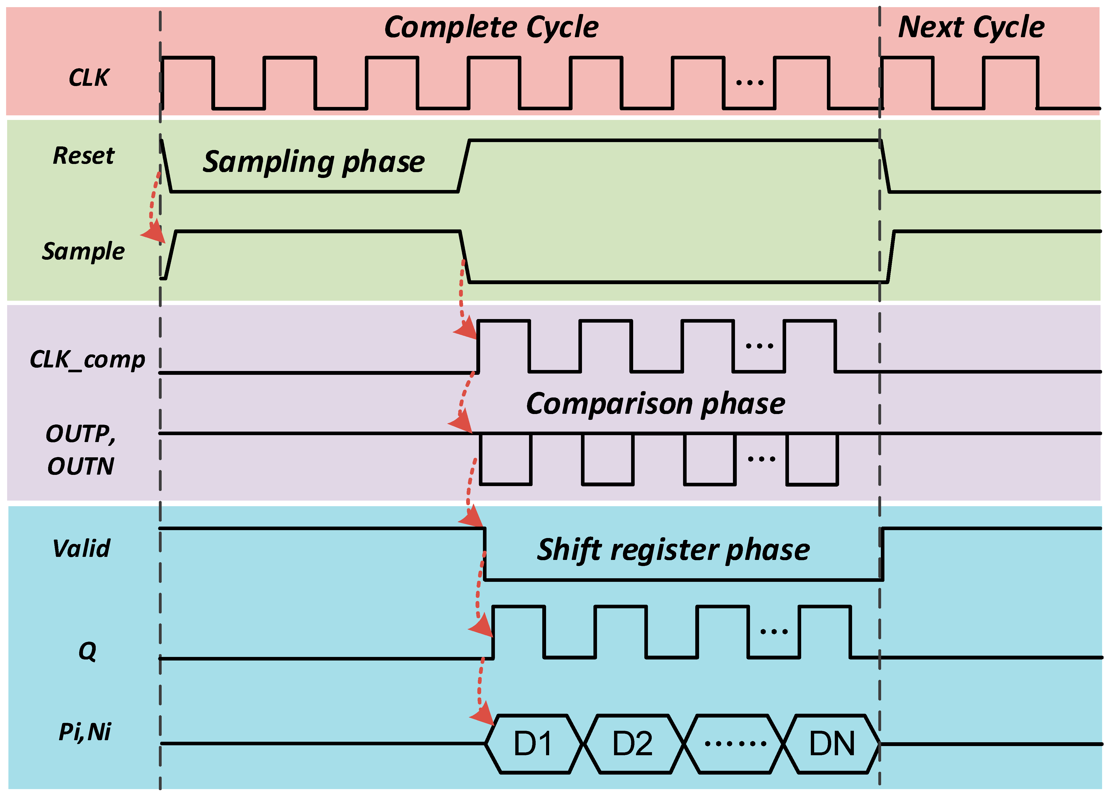
The overall sequence of the N-bit SAR ADC is shown in Figure 2. The clock signal (CLK) and the reset signal (Reset) are provided externally to enable the whole ADC to function properly. The SAR ADC operates in three phases: the sampling phase, the comparison phase, and the shift register phase. In the sampling phase, the Reset goes through a CMOS inverter to produce the sample signal (Sample). In the comparison phase, the CLK and Sample enter the comparator to generate each comparison signal (CLK_comp), after which the results of the comparison (OUTP and OUTN) are output. In the shift register phase, the Reset is used as a start signal in the first bit-slice circuit of the SAR logic, while Valid is generated by the comparison results (OUTP and OUTN), causing the SAR logic to output comparison results (Pi and Ni), and at the same time, it outputs Q signals for shifting and latching.

2.1. The Proposed Switching Scheme

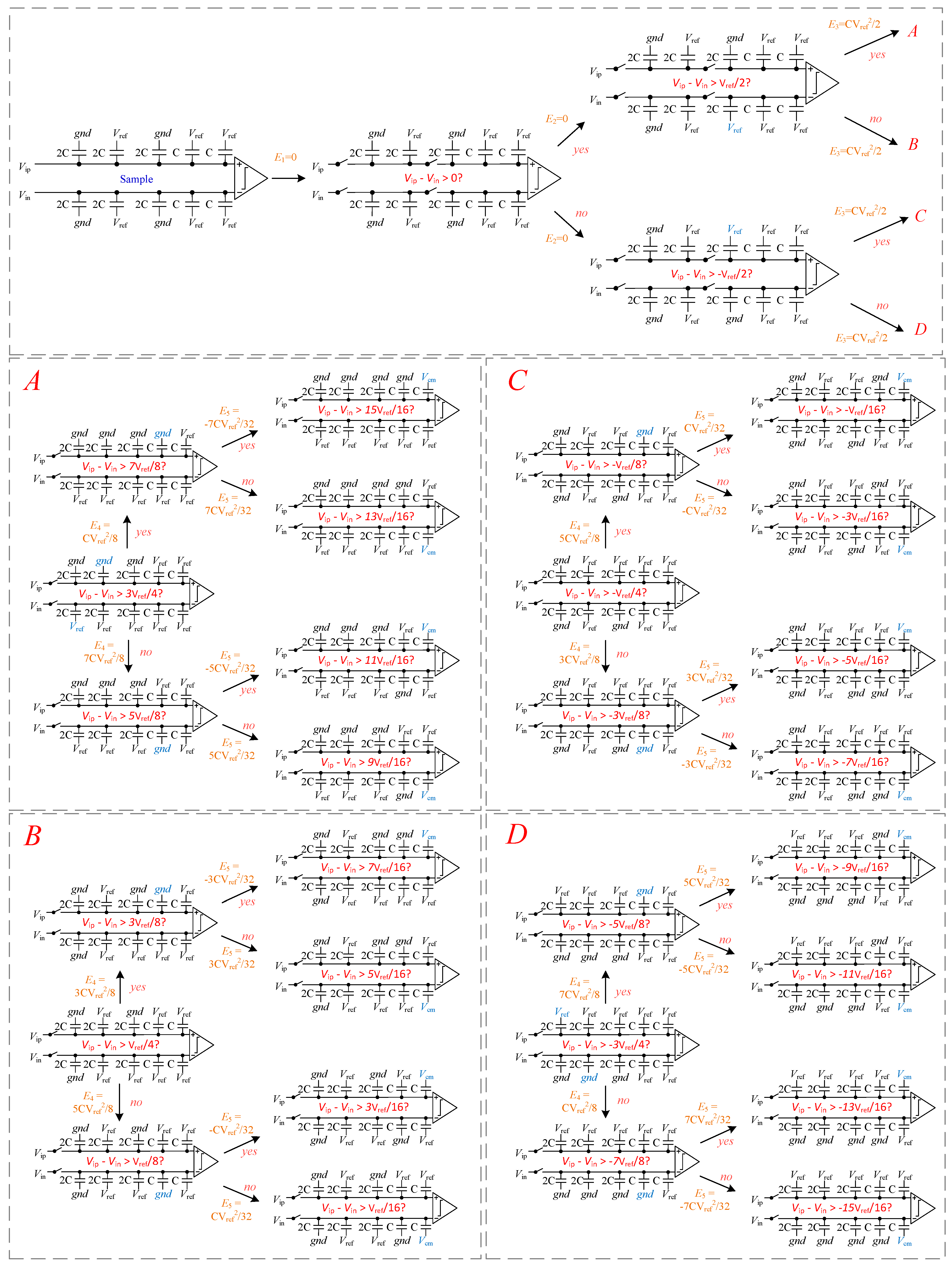
The operational rules of the proposed switching strategy are explained using a 5-bit SAR ADC. The operation consists of a sampling phase and five comparison phases, as shown in Figure 3, where the 4th comparison phase can be repeated up to N-1 times.
First comparison: The reference voltage of one of the capacitors of the subarray and the maximum capacitor of the main array is GND in the initial state, and the reference voltage of the remaining capacitors is Vref. The input signal is sampled to the top plate of the capacitor array through a sampling switch. When sampling is complete, the sampling switch is turned off. The comparator can then directly perform the first comparison and output the comparison result (D1) without consuming switching energy (E1 = 0). The voltage at the time of comparison is
V P ( 1 ) = V IP V N ( 1 ) = V IN
Second comparison: If D1 = 1, in the negative-conversion capacitor array, the reference voltage of the maximum capacitor in the main array is switched from GND to Vref; moreover, the reference voltage of the other capacitors remains constant. If D1 = 0, in the positive-conversion capacitor array, the reference voltage of the maximum capacitor in the main array is switched from GND to Vref, and the reference voltage of the other capacitors remains unchanged. Consequently, the low-side voltage increases (Vref/2), and the high-side voltage remains unchanged. The second comparison is performed, and the comparator outputs the result of the second comparison (D2). The second comparison does not consume switching energy either (E2 = 0).
The voltage of the 2nd comparison is
V P ( 2 ) = V IP + 1 D 1 × V ref 2 V N ( 2 ) = V IN + D 1 × V ref 2
Third comparison: If D1D2 = 11 or 00, in the subarray on the higher-voltage side, the reference voltage of capacitors is switched from Vref to GND, and in the subarray on the lower-voltage side, the reference voltage of capacitors is switched from GND to Vref; then, closing the bridge switch between the main array and subarray allows the capacitor array to undergo charge redistribution. If D1D2 = 10 or 01, the bridge switches are closed directly. As a result, the high-side voltage decreases (Vref/4) and the low-side voltage does not change. In the third comparison, the capacitor array switching energy is
E 3 = 2 N 6 CV ref 2
The voltage of the 3rd comparison is
V P ( 3 ) = V IN + 1 D 1 × V ref 2 D 2 × V ref 4 V N ( 3 ) = V IN + D 1 × V ref 2 1 D 2 × V ref 4
Fourth-to-(N-1)th comparisons: Based on the output of the previous step, on the higher-voltage side of the main array, the reference voltage of the corresponding capacitor is switched from Vref to GND, while the reference voltage of the other capacitors remains constant; then, the comparator performs the comparison and outputs the comparison results. The ADC repeats the process until (N-1) comparisons are completed. The switching energy for each comparison, from the 4th to the (N-1)th, is computed as follows:
E i = 2 N 1 i + j = 4 i 1 D i + D j 1 2 D i D j 1 × 2 N 1 j + 3 D i 1 + 1 2 D i 1 × 2 D 1 + D 2 × 2 N 4 × CV ref 2 2 i 1
Nth comparison: If DN-1 = 1, in the unit array of the positive-conversion capacitor array, the reference voltage of the unit capacitor is switched from Vref to Vcm, while the reference voltage of the other capacitors remains constant. If DN-1 = 0, the reference voltage of the capacitor in the unit array of the negative-conversion capacitor array is switched from Vref to Vcm, and the reference voltage of the other capacitors remains unchanged. At the Nth comparison, the capacitor array switching energy is
E N = 2 × i = 4 N 2 1 D i 1 D N 1 + D i 1 1 D N 1 × 2 N 1 j + i = 3 N 1 3 D i + 1 2 D i × 2 D 1 + D 2 × 2 N 4 2 N 2 + 1 × CV ref 2 2 N
For N-bit resolution, the average switching energy of the capacitor array is
E average = 2 N 6 + i = 5 N 2 N i 1 CV ref 2
Starting from the 3rd comparison, the voltages can all be summarized as
V P ( i ) = V IP + 1 D 1 × V ref 2 i = 3 N D i 1 × V ref 2 i 1 V N ( i ) = V IN + D 1 × V ref 2 i = 3 N 1 D i 1 × V ref 2 i 1
Figure 4a displays the successive approximation waveform, where it can be seen that the common-mode shift of the proposed switching scheme is only Vref/4. The voltage conversion flow chart of the 10-bit SAR ADC is shown in Figure 4b. Only after the first comparison does the voltage on the low-voltage side increase (Vref/2), and each subsequent comparison is a voltage drop (Vref/2i) on the high-voltage side.

2.2. Drive Circuit for DAC Capacitor Array

The switching scheme designed for DACs directly affects the complexity of the control logic, making the design of a driver circuit difficult and raising the number of transistors used. As a result, a complex control logic consumes more power, resulting in a larger percentage of power being consumed by the digital module and increasing the overall power consumption of the SAR ADC. This work designs the simplest DAC driver circuit that could reduce DAC switching energy while minimizing the use of transistors.
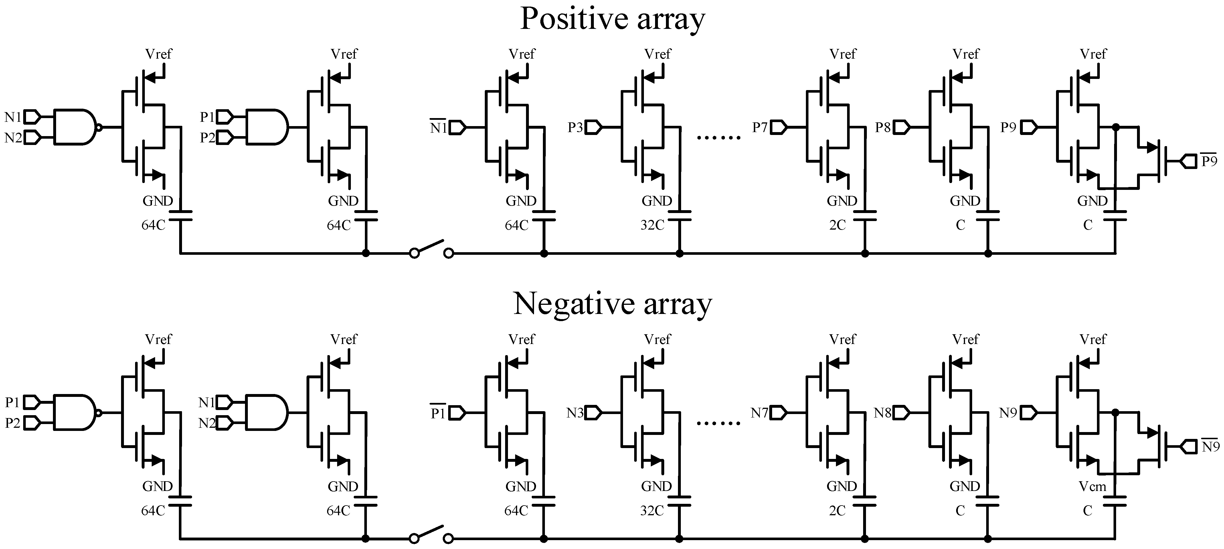
As shown in Figure 5, only two reference voltages are required per capacitor. The reference voltages of the capacitors in the main array and subarray are Vref and GND; the main array drive circuit only needs to pass through the CMOS inverter, and the capacitors in the subarray need to be controlled with AND and NAND gates, respectively. The reference voltages of the capacitors in the unit array are Vcm and GND, and the drive circuit adopts a hybrid structure comprising a CMOS inverter and a CMOS transmission gate.

2.3. Bridged Switch for DAC Capacitor Array

In order to reduce the on-resistance when bridging the capacitor array, this paper uses a new voltage bootstrap switching circuit, and the circuit structure is shown in Figure 6. The Sample signal is sampled, and the P2, N2 results are compared using the OR gate to generate the switching signal of the circuit. During the sampling phase, the Sample is high, and the bridged switch is closed at this time. At the end of sampling, P2, N2, and the Sample are low, and the bridged switch is disconnected. After the second comparison, P2 or N2 increases, closing the bridged switch.

2.4. Sampling Switch

The sampling circuitry is located at the forefront of the entire SAR ADC, and its performance level directly determines the upper limit of performance that the ADC can achieve. In order to improve the performance of sampling switches and reduce the sampling errors, bootstrapped circuits are often used for sampling switches. Bootstrapped switches improve the on-resistance stability of sampling switches [15,16]. The principle of a gate-voltage bootstrapped switch is to provide a constant gate source voltage to the MOS switch through the bootstrapped circuit when the switch is on, and the magnitude of this constant gate source voltage is close to the supply voltage.
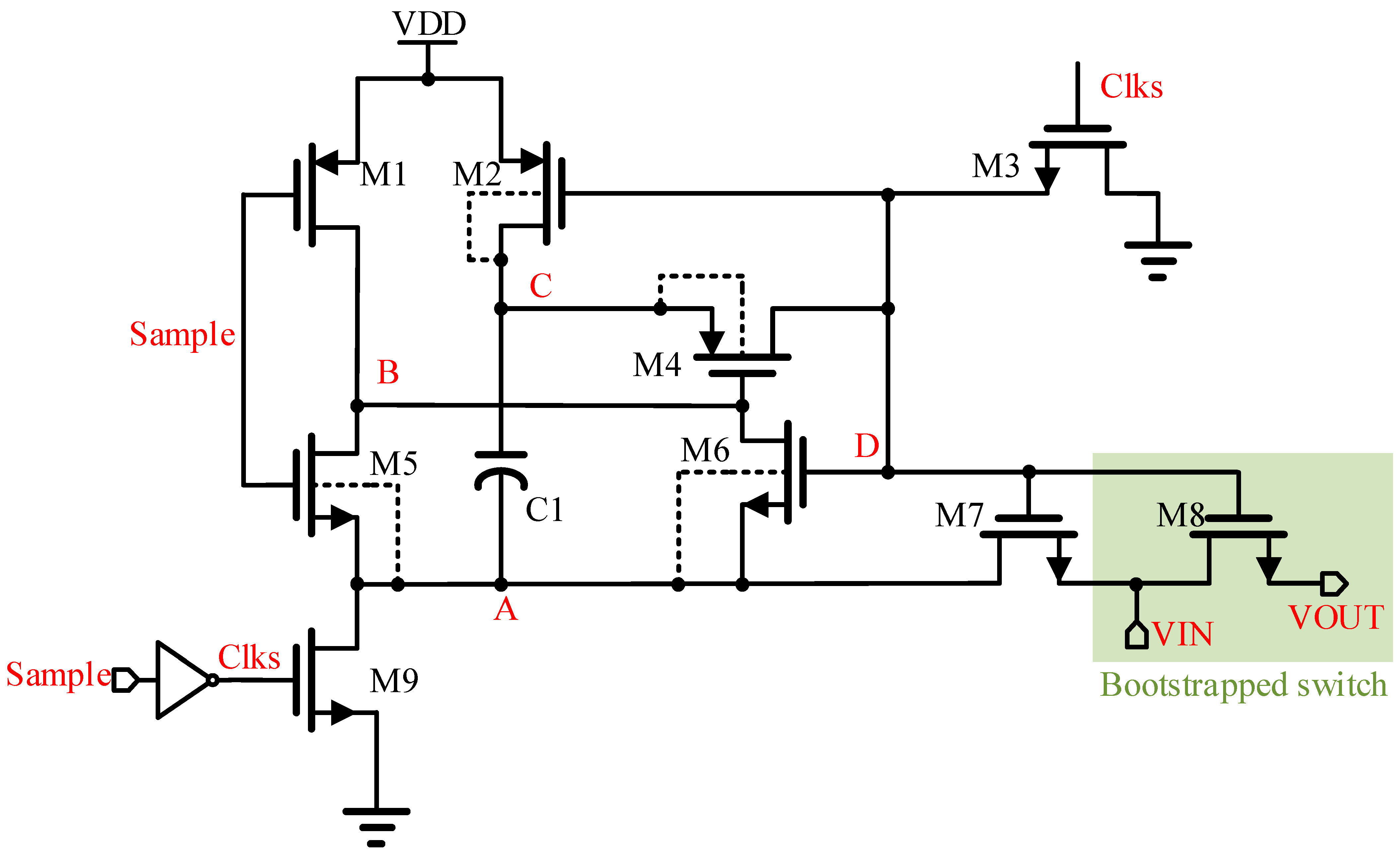
The bootstrap process consists of two phases, which are illustrated by the structure diagram shown in Figure 7. In the first stage, the sampling switch is reset when the sampling signal (Sample) is low and the CLK is high, with M1, M3, M4, and M9 being ON and M2, M5, M6, M7, and M8 being OFF. The point A and D voltages are low, and the point B and C voltages are high. In the second stage, the Sample is high; the sampling switch is closed; the CLK is low; M1, M3, M4, and M9 are OFF; M2, M5, M6, M7, and M8 are ON. The voltages at points A and D are high, and the voltages at points B and C are low. When the voltage at point A changes from ground to VIN, the voltage at point C changes from VDD to VDD + VIN, so the voltage at point D also becomes VDD + VIN.
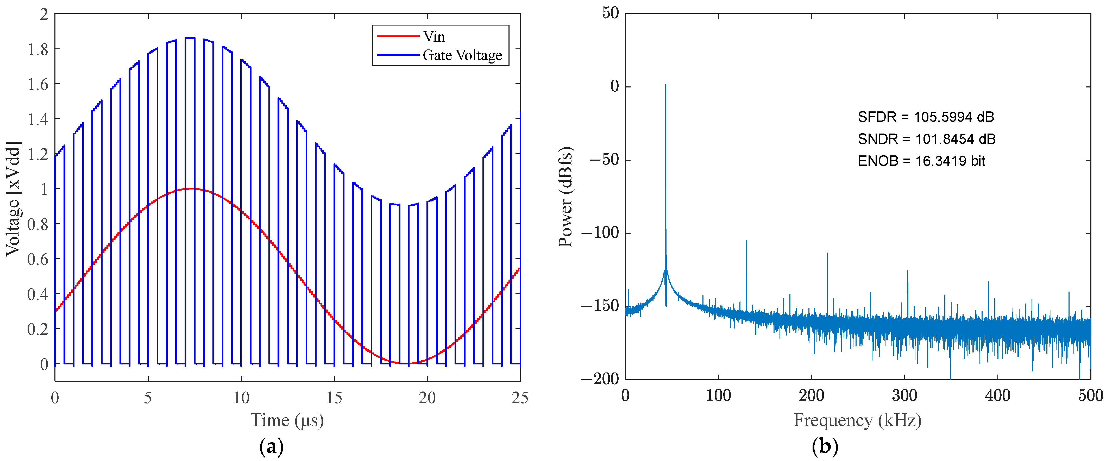
The output waveform of the input sine wave for a 100 khz clock signal is shown in Figure 8a, where it can be seen that a fixed difference between VIN and gate voltage is maintained at about VDD to ensure that the gate voltage follows the input variation. The FFT of the sampling switch is shown in Figure 8b; the SFDR and SNDR are 105.59 dB and 101.84 dB, respectively, and the ENOB is 16.39 bit, which meets the 10-bit SAR ADC requirements.

2.5. Comparator

Factors such as comparator misalignment, noise, and speed can directly affect the overall performance of SAR ADCs. Comparators are classified into static and dynamic comparators based on whether a clock signal is required to switch on and reset the comparator. Static comparators do not require a clock signal to control them, and these comparators are always in an operating state waiting for a signal to be input, thus consuming more power.
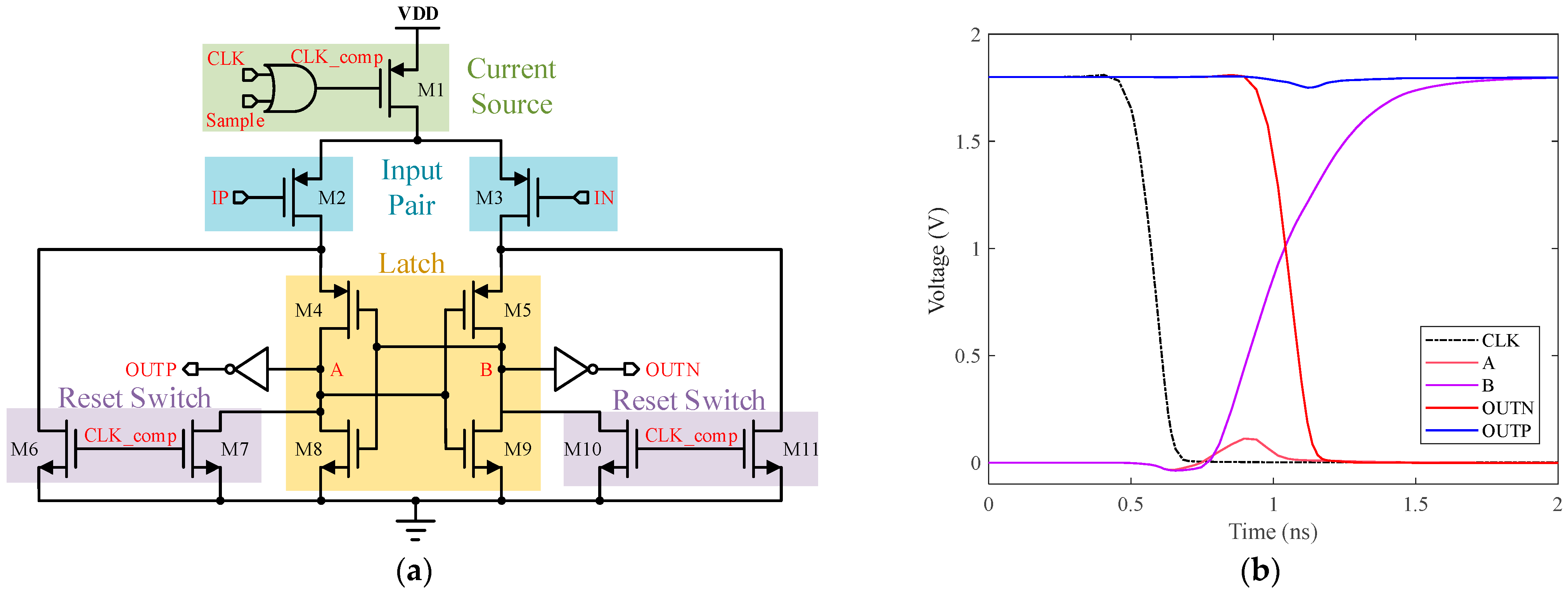
Dynamic comparators have no quiescent current, have the advantages of speed and low power consumption, and are widely used in ADCs. Usually, in comparator applications, NMOS is used as the input port of dynamic comparators [17,18,19], but in this work, PMOS is used as the input port to improve accuracy, as shown in Figure 9a. Dynamic comparators have two operating states, the reset state in the first stage and the comparison state in the second stage. In the first stage, the Sample is constant and high, so the CLK_comp, generated by the OR gate, is high. At this time, M1 is off; M6, M7, M10, and M11 are ON; A and B voltages are grounded; and OUTP and OUTN are high. In the second stage, the CLK_comp is low when the Sample is constant and low, and the CLK drops; M6, M7, M10, and M11 are OFF; VDD of A is charged via M1, M2, and M4; and VDD of B is charged via M1, M3, and M5.
If IP > IN, the A point voltage is greater than the B point voltage. M4, M5, M8, and M9 collectively constitute a positive-feedback latch circuit. Subsequently, A and B point voltages decrease and increase, respectively; OUTP increases; and OUTN decreases. If IP < IN, then eventually A and B point voltages increase and decrease, respectively, and OUTP and OUTN decrease and increase, respectively. During the comparator operation, the change from VDD to ground does not form a DC circuit; therefore, it only consumes dynamic power.
In Figure 9b, the transient simulation of the comparator is illustrated. When the CLK decreases, the voltages at A and B increase and then separate at the same time, with one increasing and the other decreasing. Ultimately, OUTP increases and OUTN decreases. The output of the comparison result is obtained by the comparator.

2.6. SAR Logic

SAR ADCs implement a successive approximation process using the SAR control logic, which continuously determines the digital output of each bit based on the output of the comparator and generates control signals to drive the switching circuitry of the capacitor array. Normally, the SAR logic has the second largest overall share of power consumption in SAR ADCs, after DAC capacitor arrays, so power optimization of the SAR logic is also necessary. The conventional SAR logic mainly consists of ring counters and shift registers, which require at least 2N flip-flops with a large number of MOS tubes and, thus, consume large amounts of power.
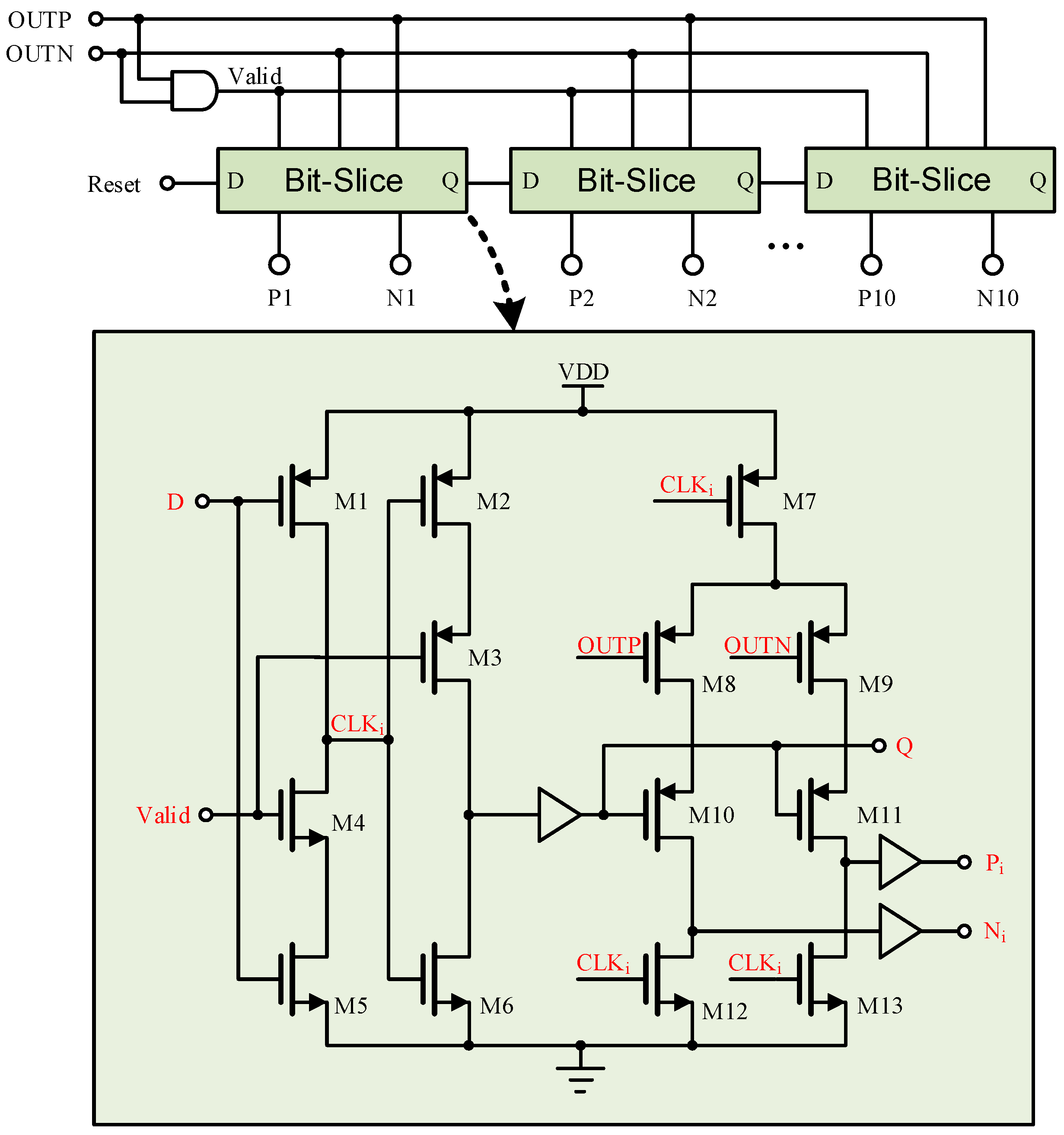
Some papers [20,21,22,23] used the dynamic SAR logic, which greatly reduces the complexity of digital circuits and avoids the use of a large number of transistors compared with the conventional SAR logic, thus greatly reducing power consumption and increasing speed. Figure 10 shows that the dynamic SAR logic consists of bit-slice circuits placed one after the other, where bit-slice circuits have the function of shifting and storing the comparison results.
During the sampling phase, the Reset is low, and both OUTP and OUTN are high, so the Valid output through the AND gate is also high; then, Pi and Ni in all bit-slice circuits are reset to “0”. When the Reset increases to indicate the end of the sampling phase, D of the first dynamic logic increases, causing CLK1 to decrease. At this point, if OUTP > OUTN, P1 increases, and N1 remains low. In contrast, if OUTP < OUTN, P1 remains low, and N1 increases. When Valid decreases, P1 and N1 of the first comparison output are latched, and Q of the initial bit-slice circuit increases to indicate that the conversion is complete. The Q of the previous bit-slice circuit is used as the D of the next bit-slice circuit, causing it to repeat the operation of the first bit-slice circuit until all 10 bits of data have been saved.

3. Results

This paper simulated 10-bit SAR ADC results for several switching schemes [7,8,9,10,11,12,13] in MATLAB. The proposed switching scheme for 10-bit SAR ADCs has an average switching energy value of 47.5 CV2ref, which is 96.52% lower than that of the conventional switching scheme. Figure 11 shows the switching energy of several switching schemes [8,9,10,11,12,13] for 10-bit output code.
Table 1 compares the characteristics of several switching schemes [8,9,10,11,12,13]. In contrast, SC [7], which splits the largest capacitor in the array into subarrays, has higher average switching energy consumption, although it has the advantage of having low complexity and no common-mode shift. MCS [8] proposed, for the first time, a top-plate sampling technique that allows the first comparison to consume no energy and reduce the area by 50%; for this reason, the response of the scientific community was significantly positive, and it became a mainstream technique for SAR ADCs adopted by most researchers. RFM [9] uses a C-2C dummy capacitor; this type of scheme is less complex, but the Vref/2 common-mode shift reduces the linearity of ADCs. VBSS [10] proposes a bidirectional single-side technique based on Vcm that uses symmetrical switching to keep a constant common-mode voltage even after the first comparison, reducing the number of common-mode shifts. SMS [11] proposes an overall shift-monotonic technique that switches one side of the capacitance to the same reference voltage in the second-comparison step without generating switching energy and a common-mode shift of only Vref/4. Tri-level [12] entails the multiple switching of the reference voltage of the same capacitor, effectively reducing the switching energy required and the area used. VMS [13] combines top-plate sampling techniques and shift-monotonic techniques from capacitor arrays, further reducing the switching energy required.
Although the average switching energy consumption of Tri-level [12] and VMS [13] is lower than that of the proposed scheme, they have the disadvantages of high control logic complexity and high dependence on Vcm accuracy, which increases the power consumption of the SAR ADC digital module. In this work, the proposed switching scheme makes use of top-plate sampling, charge recycling, and bridge switching; reduces switching energy consumption without increasing the complexity of the control logic; and has a common-mode shift of only Vref/4.
The simulation of the proposed 10-bit SAR ADC was carried out using the HPZ228 workstation using IC617 with the following parameter settings: the CMOS was 180 nm; the power supply was 1.8 V; and the sampling rate was 1 MS/s. ENOB, SNDR, SFDR are the ADCs’ dynamic characteristic parameters that are dependent on the input signal. Therefore, in this work, we performed a simulation at the full-swing input signal frequency of 433.33 kHz, and the FFT spectrum is shown in Figure 12a. The proposed SAR ADC achieved 9.8-bit ENOB, 60.76 dB SNDR, and 69.85 dB SFDR.
DNL is the maximum value of the difference between two adjacent scales of an ADC, and INL is the degree of deviation of the actual converted level from the ideal converted level. Both DNL and INL are static characteristic parameters of ADCs; hence, in this work, we performed a simulation at the input frequency of 43.33 kHz, as shown in Figure 12b. The peak values of DNL and INL were −0.16/0.14 LSB and −0.25/0.11 LSB, both of which are less than 0.5 LSB.
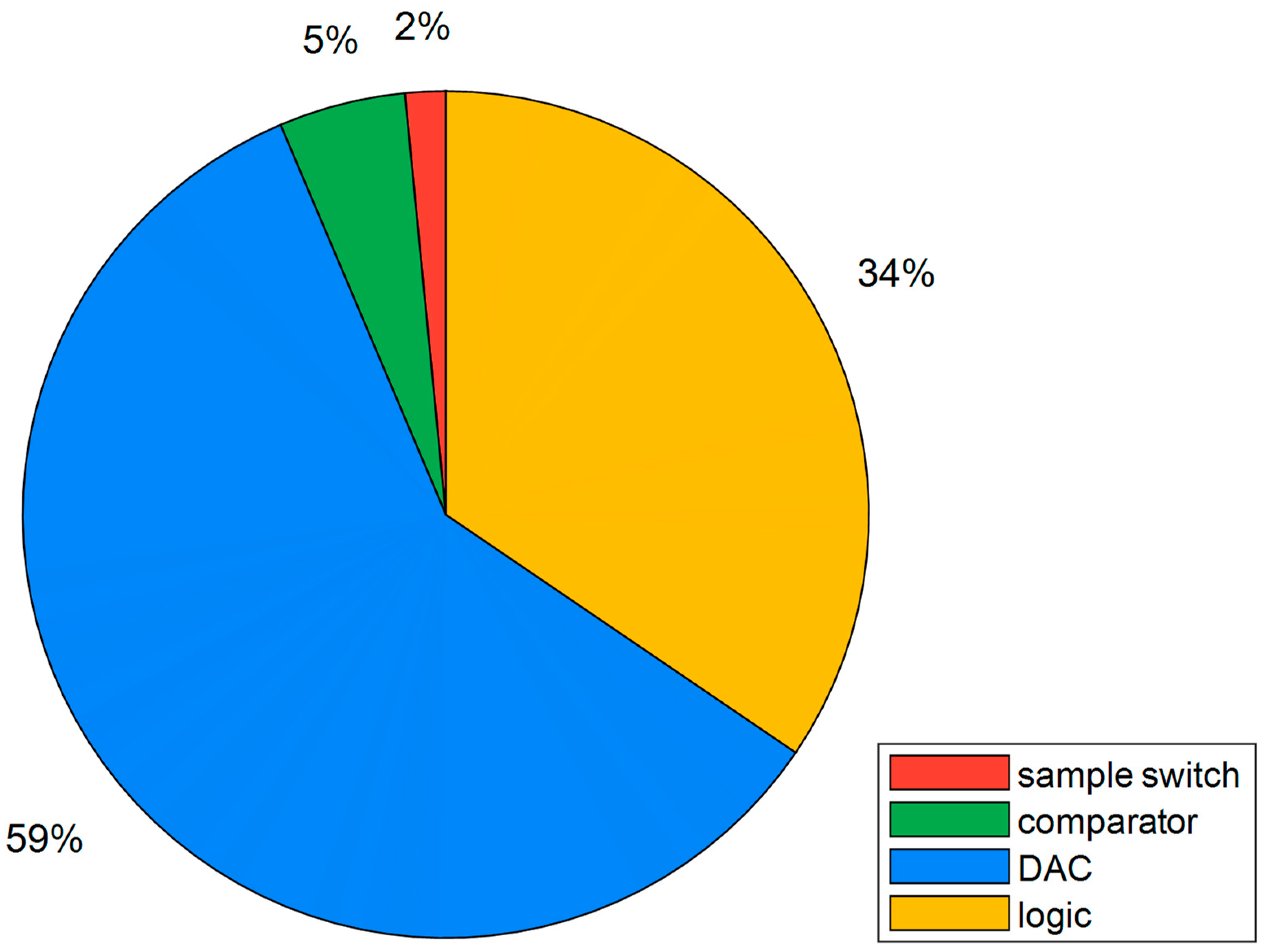
Figure 13 shows the percentage of the total power consumed by each key circuit module of the proposed SAR ADC, with the DAC accounting for 59%; the SAR logic accounting for 34%; the comparator accounting for 5%; and the sampling switches accounting for 2%. The total power consumption was 14.7 μW. Table 2 shows a performance comparison of several ADCs proposed in recent years [6,24,25,26,27]. The FoM was used to compare the power utility of different ADCs. This work reduced the FoM to 16.55 fJ/conv.-step; hence, the proposed SAR ADC is more competitive.

4. Conclusions

This paper presents a bridged-switch energy-efficient switching scheme for SAR ADCs with a low-complexity capacitor drive circuit. In the proposed switching scheme, top-plate sampling technology, closed-loop charge recovery technology, and bridged-switch technology are adopted, and only the last capacitor uses reference voltage Vcm. As a result, the DAC has lower switching-energy consumption, low drive circuit complexity, and low dependence on Vcm. In the proposed switching scheme, the average switching energy is 47.5 CV2ref, which is 96.52% lower and reduces the area by 75% compared with the conventional switching scheme. The key circuit modules to reduce the power consumption of the SAR ADC are a full dynamic comparator, bootstrapped switches, and dynamic SAR logic. The proposed 10-bit SAR ADC was simulated under the conditions of 180 nm CMOS process and 1 MS/s, resulting in an SNDR of 60.76 dB, an SFDR of 69.85 dB, power consumption of 14.7 μW, and an FoM of 16.55fJ/conv.-step. In this paper, although bridge switches are used, the ADC is not designed as a bit-adjustable ADC. So, in future work, an ADC could be designed as a bit-adjustable ADC by using bridge switches to extend the application area of ADCs.

Author Contributions

Conceptualization, Y.H.; methodology, Y.H.; software, Y.H. and B.T.; validation, Y.H., B.T. and L.H.; formal analysis, Y.H.; investigation, Q.H. and J.C.; resources, Y.H., B.L. and Z.W.; data curation, B.T. and C.C.; writing—original draft preparation, Y.H. and B.T.; writing—review and editing, C.C., L.H. and Q.H.; visualization, B.T., J.C. and J.X.; supervision, Y.H.; project administration, Y.H. and Z.W.; funding acquisition, B.L. and Y.H. All authors have read and agreed to the published version of the manuscript.

Funding

This work was funded by the National Natural Science Foundation of China (No. 60976026), the Key Field Project of Colleges and Universities in Guangdong Province (No. 2021ZDZX1081), the Key Project of Social Welfare and Basic Research Project in Zhongshan City (2021B2020), the Construction Project of Professional Quality Engineering in 2020 (No. YLZY202001), and the Construction Project of Professional Quality Engineering in 2021 (No. JD202101).

Institutional Review Board Statement

Not applicable.

Informed Consent Statement

Not applicable.

Data Availability Statement

The data presented in this study are available on request from the corresponding author. The data are not publicly available due to privacy.

Conflicts of Interest

The authors declare no conflict of interest.

Nomenclature

IoT: Internet of Things; SAR ADC: successive approximation register analog-to-digital converter; LSB: least significant bit; CMOS: Complementary Metal Oxide Semiconductor; ENOB: effective number of bits; SNDR: signal-to-noise and distortion ratio; SFDR: spurious-free dynamic range; FoM: figure of merit; DAC: digital-to-analog converter.

References

  1. Chung, Y.-H.; Zeng, Q.-F. A 12-Bit 100-kS/s SAR ADC for IoT Applications. In Proceedings of the 2020 International Symposium on VLSI Design, Automation and Test (VLSI-DAT), Hsinchu, Taiwan, 10–13 August 2020; pp. 1–4. [Google Scholar]
  2. Zhao, X.; Li, D.; Zhang, X.; Liu, S.; Zhu, Z. A 0.6-V 94-nW 10-Bit 200-kS/s Single-Ended SAR ADC for Implantable Biosensor Applications. IEEE Sens. J. 2022, 22, 17904–17913. [Google Scholar] [CrossRef]
  3. Hu, Y.; Hu, L.; Tang, B.; Li, B.; Wu, Z.; Liu, X. A 100 KS/s 8–10-Bit Resolution-Reconfigurable SAR ADC for Biosensor Applications. Micromachines 2022, 13, 1909. [Google Scholar] [CrossRef] [PubMed]
  4. Begum, F.; Mishra, S.; Islam, M.N.; Dandapat, A. A 10-Bit 2.33 fJ/Conv. SAR-ADC with High Speed Capacitive DAC Switching Using a Novel Effective Asynchronous Control Circuitry. Analog. Integr. Circ. Signal Process 2019, 100, 311–325. [Google Scholar] [CrossRef]
  5. Jian, M.; Zheng, J.; Kong, X.; Yuan, M.; Zhang, C.; Guo, C.; Sun, B. A 12-Bit SAR ADC with a Reversible VCM-Based Capacitor Switching Scheme. Microelectron. J. 2022, 129, 105588. [Google Scholar] [CrossRef]
  6. Tong, X.; Zhao, S.; Xin, X. High Energy Efficiency and Linearity Switching Scheme without Reset Energy for SAR ADC. Circuits Syst. Signal Process 2022, 41, 5872–5894. [Google Scholar] [CrossRef]
  7. Ginsburg, B.P.; Chandrakasan, A.P. An Energy-Efficient Charge Recycling Approach for a SAR Converter with Capacitive DAC. In Proceedings of the 2005 IEEE International Symposium on Circuits and Systems, Kobe, Japan, 23–26 May 2005; pp. 184–187. [Google Scholar]
  8. Liu, C.-C.; Chang, S.-J.; Huang, G.-Y.; Lin, Y.-Z. A 10-Bit 50-MS/s SAR ADC With a Monotonic Capacitor Switching Procedure. IEEE J. Solid State Circuits 2010, 45, 731–740. [Google Scholar] [CrossRef]
  9. Wang, H.; Zhu, Z. Energy-Efficient and Reference-Free Monotonic Capacitor Switching Scheme with Fewest Switches for SAR ADC. IEICE Electron. Express 2015, 12, 20141202. [Google Scholar] [CrossRef]
  10. Huang, L.; Li, J.; Jiang, X.; Wu, J. A 2.1-fJ/Conversion-Step 10-Bit 125-KS/s SAR ADC with Vcm-Based Bidirectional Single-Side Switching Scheme. In Proceedings of the 2023 12th International Conference on Modern Circuits and Systems Technologies (MOCAST), Athens, Greece, 28–30 June 2023; pp. 1–4. [Google Scholar]
  11. Hsieh, S.-E.; Hsieh, C.-C. A 0.3-V 0.705-fJ/Conversion-Step 10-Bit SAR ADC With a Shifted Monotonic Switching Procedure in 90-Nm CMOS. IEEE Trans. Circuits Syst. II Express Briefs 2016, 63, 1171–1175. [Google Scholar] [CrossRef]
  12. Yuan, C.; Lam, Y. Low-Energy and Area-Efficient Tri-Level Switching Scheme for SAR ADC. Electron. Lett. 2012, 48, 482–483. [Google Scholar] [CrossRef]
  13. Zhu, Z.; Xiao, Y.; Song, X. VCM-Based Monotonic Capacitor Switching Scheme for SAR ADC. Electron. Lett. 2013, 49, 327–329. [Google Scholar] [CrossRef]
  14. Hu, Y.; Liu, A.; Li, B.; Wu, Z. Closed-loop Charge Recycling Switching Scheme for SAR ADC. Electron. Lett. 2017, 53, 66–68. [Google Scholar] [CrossRef]
  15. Abo, A.M.; Gray, P.R. A 1.5-V, 10-Bit, 14.3-MS/s CMOS Pipeline Analog-to-Digital Converter. IEEE J. Solid State Circuits 1999, 34, 599–606. [Google Scholar] [CrossRef]
  16. Yuan, F. Bootstrapping Techniques for Energy-Efficient Successive Approximation ADC. Analog. Integr. Circ. Signal Process 2023, 114, 299–313. [Google Scholar] [CrossRef]
  17. Schinkel, D.; Mensink, E.; Klumperink, E.; Van Tuijl, E.; Nauta, B. A Double-Tail Latch-Type Voltage Sense Amplifier with 18ps Setup+Hold Time. In Proceedings of the 2007 IEEE International Solid-State Circuits Conference, Digest of Technical Papers, San Francisco, CA, USA, 11–15 February 2007; pp. 314–605. [Google Scholar]
  18. Savani, V.; Devashrayee, N.M. Analysis and Design of Low-Voltage Low-Power High-Speed Double Tail Current Dynamic Latch Comparator. Analog. Integr. Circ. Signal Process 2017, 93, 287–298. [Google Scholar] [CrossRef]
  19. Babayan-Mashhadi, S.; Lotfi, R. Analysis and Design of a Low-Voltage Low-Power Double-Tail Comparator. IEEE Trans. VLSI Syst. 2014, 22, 343–352. [Google Scholar] [CrossRef]
  20. Harpe, P.J.A.; Zhou, C.; Bi, Y.; Van Der Meijs, N.P.; Wang, X.; Philips, K.; Dolmans, G.; De Groot, H. A 26 μW 8 Bit 10 MS/s Asynchronous SAR ADC for Low Energy Radios. IEEE J. Solid State Circuits 2011, 46, 1585–1595. [Google Scholar] [CrossRef]
  21. Zhu, Z.; Xiao, Y.; Wang, W.; Wang, Q.; Yang, Y. A 0.6 V 100 KS/s 8–10 b Resolution Configurable SAR ADC in 0.18 Μm CMOS. Analog. Integr. Circ. Signal Process 2013, 75, 335–342. [Google Scholar] [CrossRef]
  22. Zhu, Z.; Xiao, Y.; Liang, L.; Liu, L.; Yang, Y. A 3.03 μW 10-BIT 200 KS/s SAR ADC IN 0.18 μM CMOS. J. Circuit. Syst. Comp. 2013, 22, 1350026. [Google Scholar] [CrossRef]
  23. Zhu, Z.; Qiu, Z.; Liu, M.; Ding, R. A 6-to-10-Bit 0.5 V-to-0.9 V Reconfigurable 2 MS/s Power Scalable SAR ADC in 0.18 μM CMOS. IEEE Trans. Circuits Syst. I Regul. Pap. 2015, 62, 689–696. [Google Scholar] [CrossRef]
  24. He, X.; He, J.; Cai, M.; Jing, Z. A Low Power Switching Method with Variable Comparator Reference Voltage and Split Capacitor Array for SAR ADC. In Proceedings of the 2016 IEEE International Conference on Electron Devices and Solid-State Circuits (EDSSC), Hong Kong, China, 3–5 August 2016; pp. 379–382. [Google Scholar]
  25. Rasool Ghasemi, A.; Saberi, M.; Lotfi, R. A Low-Power Capacitor Switching Scheme with Low Common-Mode Voltage Variation for Successive Approximation ADC. Microelectron. J. 2017, 61, 15–20. [Google Scholar] [CrossRef]
  26. Zha, Y.; Zahnd, L.; Deng, J.; Ruffieux, D.; Badami, K.; Mavrogordatos, T.; Matsuo, Y.; Emery, S. An Untrimmed PVT-Robust 12-Bit 1-MS/s SAR ADC IP in 55nm Deeply Depleted Channel CMOS Process. In Proceedings of the 2019 IEEE Asian Solid-State Circuits Conference (A-SSCC), Macau, China, 4–6 November 2019; pp. 13–16. [Google Scholar]
  27. Sotoudeh, M.; Rezaei, F. A Four-Level Switching Scheme for SAR ADCs with 87.5% Area Saving and 97.85% Energy-Reduction. Circuits Syst. Signal Process 2020, 39, 4792–4809. [Google Scholar] [CrossRef]
Figure 1. The proposed architecture of the N-bit SAR ADC.
Applsci 13 12897 g001
Figure 2. The sequence chart of the N-bit SAR ADC.
Applsci 13 12897 g002
Figure 3. Switching stage of the proposed 5-bit SAR ADC.
Applsci 13 12897 g003
Figure 4. Diagram of voltage change: (a) waveform of the proposed switching scheme; (b) flow chart of the 10-bit SAR ADC.
Applsci 13 12897 g004
Figure 5. Drive circuit for DAC capacitor array.
Applsci 13 12897 g005
Figure 6. Bridged switch for DAC capacitor array.
Applsci 13 12897 g006
Figure 7. Bootstrapped sampling switch.
Applsci 13 12897 g007
Figure 8. (a) Transient simulation of sampling switch; (b) FFT of sampling switch.
Applsci 13 12897 g008
Figure 9. (a) Dynamic comparator; (b) transient simulation of dynamic comparator.
Applsci 13 12897 g009
Figure 10. Dynamic SAR logic.
Applsci 13 12897 g010
Figure 11. Switching energy for 10-bit output code. The blue [8], yellow [9], haze blue [10], green [11], black [12], red [13], and magenta curves are switching energy.
Applsci 13 12897 g011
Figure 12. The performance of the proposed SAR ADC: (a) FFT of SAR ADC; (b) DNL and INL of SAR ADC.
Applsci 13 12897 g012
Figure 13. Power consumption distribution of the proposed SAR ADC.
Applsci 13 12897 g013
Table 1. Comparison of switching schemes for 10-bit SAR ADCs.
Switching
Scheme
Average Switching
Energy (CV2ref)
Energy
Saving
Area
Reduction
Control Logic
Complexity
Dependency on
the Accuracy of Vcm
Common-Mode Shift
Conventional1363.3ReferenceReferenceLowNo0
SC [7]852.337.48%0%LowNo0
MCS [8]255.581.26%50%LowNoVref/2
RFM [9]12890.61%74.7%LowNoVref/2
VBSS [10]69.0894.93%75%LowVery highVref/4
SMS [11]63.7595.32%75%LowVery highVref/4
Tri-level [12]42.4196.89%75%HighVery high (all bits
except MSB)
Vref/2
VMS [13]31.8897.66%75%HighVery high (all bits
except MSB)
Vref/4
Proposed47.596.52%75%LowVery low (only LSB)Vref/4
Table 2. Performance comparison.
Parameter[24] *[25] *[26][27] *[6] *This Work *
Year201620172019202020222023
Process (nm)18018055130180180
Resolution (bits)8101281010
Sampling rate (MS/s)111111
Supply voltage (V)1.21.80.5/0.91.211.8
SNDR (dB)48.05616847.1257.8160.76
SFDR (dB)-79.8-57.3668.6369.85
ENOB (bits)7.699.84-7.549.319.8
DNL (LSB)−0.14/0.68-−0.58/0.60−0.24 /0.26-−0.16/0.14
INL (LSB)−0.31/0.48-−0.81/0.58−0.28/0.26-−0.25/0.11
Power consumption (μW)8.1435.33011. 5615.2514.7
FoM 1 (fJ/conv.-step)3938.5224.562.112016.55
* Simulated results. 1 FoM = Power/(2ENOB × fsampling).
Disclaimer/Publisher’s Note: The statements, opinions and data contained in all publications are solely those of the individual author(s) and contributor(s) and not of MDPI and/or the editor(s). MDPI and/or the editor(s) disclaim responsibility for any injury to people or property resulting from any ideas, methods, instructions or products referred to in the content.