1. Introduction
One-dimensional photonic-crystal microresonators (MCRs) have attracted the close attention of researchers in recent years, which is largely due to their wide use in various optical devices for the selective separation and amplification of an optical signal based on the interaction of optical modes in MCRs and resonances in the active medium that fills its cavity [
1,
2,
3,
4,
5]. The possibility of the controlled tuning of the resonant frequency of the microresonator by changing the external parameters is important for many practical applications. The efficient rearrangement of the MCR transmission and reflection spectra can be achieved by introducing layers into the cavity between the mirrors, the material parameters of which depend on easily changeable external factors [
6,
7,
8,
9]. MCR’s schemes are used to create a wide class of radiation control devices (switches, modulators, filters), performing the function of amplifying various types of light interaction with the propagation medium [
10,
11,
12,
13,
14,
15,
16,
17].
To form a symmetric microresonator, two identical Bragg mirrors (BMs) are required with a change in the order of the layers in one of them. The area between the mirrors (the working cavity), as a rule, is filled with an active medium. If the distance between the BMs is a multiple of half the wavelength of the propagating radiation, standing waves (resonator modes) are established in the working cavity of the MCR, and transmission resonances are observed in the photonic band gaps (PBGs).
The graphene monolayer is one of the most promising photonics materials and various planar structures are based on it. Graphene monolayer, being a 2D structure, has a number of unique properties such as zero band gap, high electron mobility, high optical transparency and mechanical strength [
18,
19]. The chemical modification of graphene structures makes it possible to obtain structures with a non-zero band gap: the fluorination of graphene makes it possible to obtain a dielectric with a band gap of 3 eV [
20]; doping with nitrogen and boron makes it possible to obtain n- and p-type semiconductors [
21]; and partial hydrogenation leads to the manifestation of ferromagnetic properties in graphene [
22]. Unique mechanical and electronic properties make graphene a promising candidate for creating flexible electronic devices, field-effect transistors, solar cells and energy storage devices. In this regard, the practical application of graphene and other 2D materials is currently one of the priority areas of both fundamental and applied research [
23,
24].
In addition to chemical modification, the parameters of graphene-containing structures can be effectively controlled by changing its chemical potential (Fermi energy) using an applied voltage [
25,
26,
27,
28]. Graphene monolayers with an inverse population of charge carriers, realized as a result of optical, injection, or diffusion pumping, are the active layers of a medium that amplifies THz radiation. However, the creation of an inverse population is associated with a number of fundamental and technical difficulties (to achieve amplification, a long-lived inverse population is required, which, in turn, requires the creation of high-purity graphene samples). Therefore, alternative mechanisms are of interest to implement the amplification of THz radiation in graphene. It was shown in [
29,
30,
31,
32,
33] that graphene with charge carrier drift has the properties of an amplifying medium, i.e., graphene in the active state can be obtained using current pumping. At carrier drift velocities that are greater than the phase velocity of an electromagnetic wave, the real part of graphene conductivity becomes negative, and amplification is achieved in the THz range due to the Vavilov–Cherenkov effect.
In this work, based on the matrix approach for a symmetric MCR structure with dielectric BMs, expressions for the transmission and reflection coefficients are obtained and their frequency dependencies are presented for the various values of the static magnetic field and the Fermi energy of graphene monolayers. For comparison, the features of the spectra are studied for an MCR with an unfilled and a filled cavity. The working cavity is filled with a structure consisting of several “dielectric-graphene” or “semiconductor-graphene” periods with controlled material parameters. is considered the material of semiconductor layers, the choice of which is associated with the highest mobility and mean free path of electrons (up to 78,000 cm/V · s and 0.7 m at 300 K) among all known semiconductor materials. We consider a structure with wide possibilities of controlling the transmission and reflection spectra, provided that amplification is achieved in the terahertz range, in contrast to the above works.
2. Material Parameters of the Structure
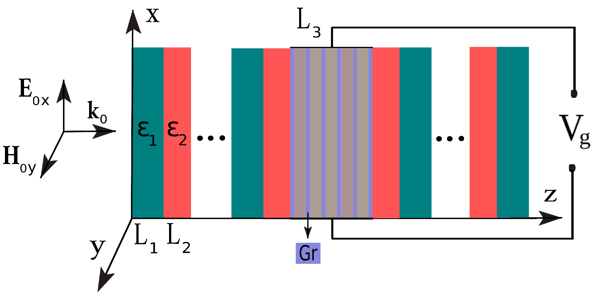
Let us consider a symmetric microresonator structure formed of two BMs and a resonator cavity separating them, designed to be filled with a controlled active structure (As can be seen
Figure 1).
We assume that the period of the BMs consists of two layers of isotropic dielectrics
and
with permittivities
and
, and with the same optical thicknesses
. Each of the Bragg mirrors consists of
a periods
. The cavity has a length
and permittivity
. We also assume that the permittivity of the coating medium and substrate
. For a microresonator with a free cavity, the transfer matrix that relates the wave field at the input and output of the structure has the form:
where the transfer matrices of individual layers has the form:
where
,
are propagation constants in the respective layers,
and
and
c are the frequency and speed of the wave in a vacuum, respectively. The transmission and reflection amplitude coefficients for the entire MCR structure are determined in terms of the matrix elements of the transfer matrix:
The energy transmission and reflection coefficients in the case of a symmetrical environment (we assume that the structure is in a vacuum) have the form , . When the absorption in the layers is taken into account, the fraction of the energy absorbed by the structure is determined by the quantity . The negativity of absorption should indicate the presence of amplification in the structure.
To reveal the spectral features of an MCR that arises when a cavity is filled with an effective medium, we first consider the distribution of the wave field in a structure with an unfilled cavity.
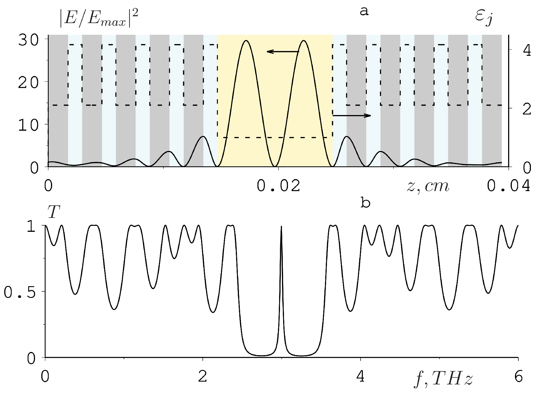
Figure 2 shows the distribution of the dielectric permittivity and the squared modulus of the electric field strength of the TM wave (solid and dashed lines) along the structure, and (bottom) shows the transmission spectrum for the considered resonator structure with the number of periods in BMs
. In the numerical analysis, the following values of the structure parameters are used:
and
, the optical thickness of the layers
m, the real thicknesses of the layers in the BMs
m and
m, period is
m, the cavity has a length
m, and permittivity
, the operating frequency
= 3 THz,
m. It can be seen that, for the chosen parameters, the amplitude of the electric field is minimal at the center of the cavity and reaches a maximum at its lateral boundaries.
The photonic band gap (PBG) exists in the transmission spectrum in the region of the operating frequency in the center of which a defect mode is observed—a narrow peak of almost complete transmission, associated with violation of the structure periodicity. In BMs, the transmission maximum corresponds to the center frequency of the non-transmission zone of a defect-free structure when the optical thicknesses of the layers are equal. The symmetry of the structure with respect to the location of the defect (in this case, the role of the defect is played by an unfilled cavity) leads to the maximum possible value of the transmittance in the defect mode. The spectral width of the defect mode essentially depends on the value of the layers’ permittivity in the region of the defect. The width of the transmission miniband for a structure with an increased permittivity in the region of a defect is much wider than for a structure with a reduced value. An increase in the number of periods a in BMs leads to sharper band gaps and the narrowing of the spectral line of the defect mode, but does not affect its position in the transmission spectrum and the magnitude of the maximum . In this case, the degree of field localization in the region of the defect significantly increases. Thus, with an increase in the number of periods in BMs by two (one each to the left and to the right of the cavity), the square of the field amplitude at the maximum doubles, i.e., .
Then, we will consider an MCR with a cavity filled with a periodic structure of alternating layers of dielectric (or semiconductor) and graphene monolayer with thicknesses
(or
) and
. The material parameters of each layer in the studied frequency range are scalar-tensor quantities: for the dielectric and graphene, the permittivities
and
; for semiconductor
, the magnetic permeability of all layers in the studied range can be considered equal to unity. Such a one-dimensional structure has the properties of a uniaxial crystal with a symmetry axis perpendicular to the layer interfaces (
axis). The transfer matrix of the insert has the form
, where
for dielectric and semiconductor layers, parameter b specifies the number of periods. In this case, the transfer matrices
and
have the form of a matrix (
2) with the corresponding permittivities.
For semiconductor layers in the case of an external magnetic field oriented along the
axis, the nonzero components of the semiconductor permittivity tensor
,
,
depend on frequency and field as follows [
34]:
where
and
are the plasma and cyclotron frequencies of the semiconductor,
is the lattice part of the permittivity,
e is the charge of an electron,
and
are the concentration and the effective mass of the carriers, respectively,
and
is a relaxation parameter. The eigenwaves of the semiconductor medium are
and
waves at the specified orientation of the magnetic field and the transverse propagation of the electromagnetic wave (
). Further analysis will be carried out for a
-type wave, since it is a wave of this type that is controlled by an external field. The propagation constant of this wave
, where
and
is the effective permittivity.
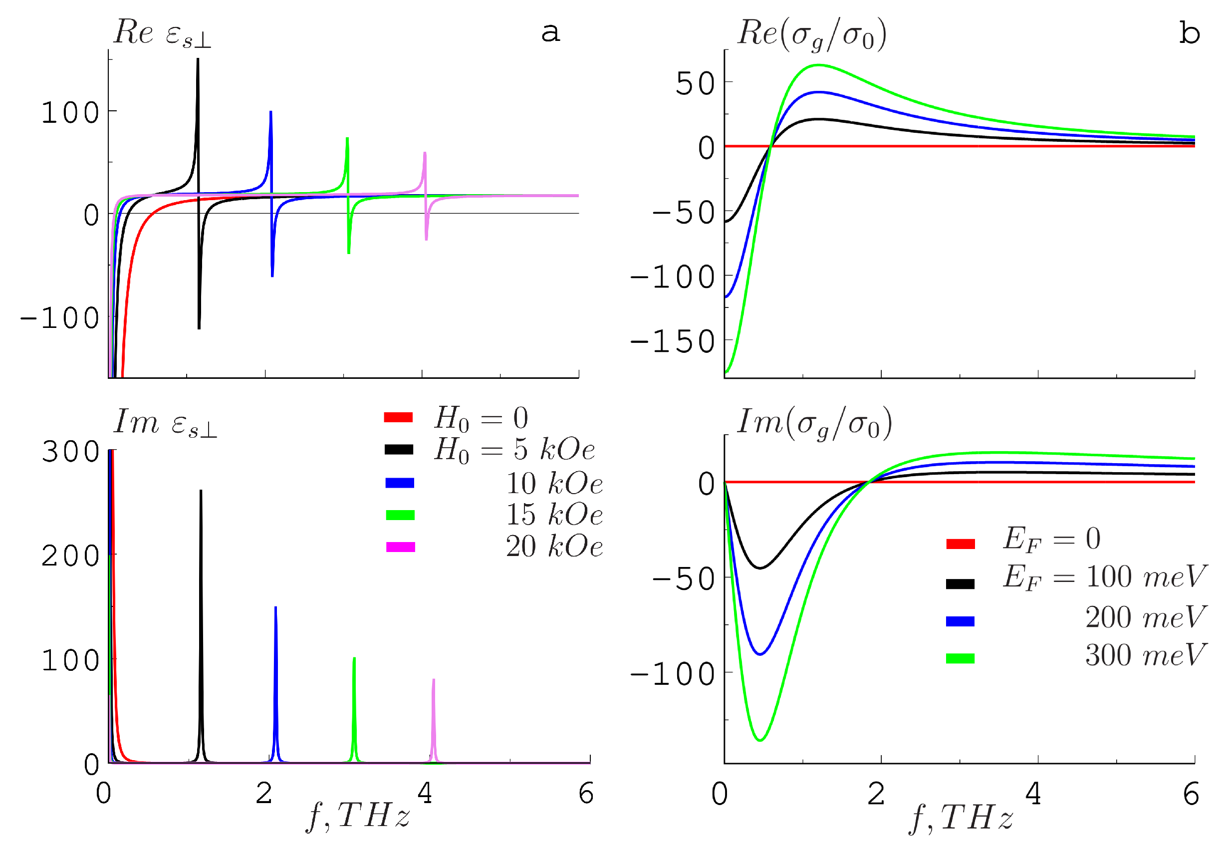
Figure 3a shows the frequency dependencies of the real and imaginary parts of the effective permittivity for the
semiconductor, obtained at
kOe (black, red, blue, green, violet curves, color online only) and the values of the parameters used in the numerical analysis:
,
,
= 10
cm
,
= 3.5 · 10
s
,
= 5 · 10
s
. We note the resonant character of these dependencies: for each value
in a narrow region near the frequency
, a sharp increase in the imaginary part of the effective permittivity is observed, which should lead to sharp dips in the transmission spectrum for the semiconductor layer at these frequencies. Increasing the magnetic field shifts the resonant peak to higher frequencies and lowers the height of the resonant peak. It can be seen that the magnetic field can be used to effectively control the permittivities of the semiconductor layers.
Graphene monolayers can be both in the unexcited and active states. In unexcited graphene, the Fermi energy (chemical potential) is at the Dirac point and is equal to zero. In this case, the valence band is completely filled, the conduction band is completely free, and the band gap is absent. The chemical potential can be shifted into the conduction band or valence band and thereby change the surface conductivity of the graphene sheet by applying a voltage of different polarity between the graphene monolayer and the substrate. A planar magnetic field does not affect the electronic subsystem of graphene due to its 2D geometry.
The terahertz response of graphene for frequencies below the electron–electron collision frequency is determined by its conductivity. The expression for the conductivity of graphene, which is valid for the region
f < 5 THz and obtained using the hydrodynamic approach when solving the equations of the electromagnetic field, the balance of momentum and energy of charge carriers, as well as the continuity equation, has the form [
32,
33]:
where
is the surface static conductivity,
e is the charge of an electron,
ℏ is Planck’s constant and
is the momentum relaxation time of charge carriers in the graphene monolayer,
,
u is the charge carrier drift velocity and the Fermi velocity in graphene
= 10
m/s,
is the Fermi energy (or chemical potential) in graphene. The following notation is also introduced:
,
,
,
,
. Graphene conductivity (5) in the hydrodynamic regime was obtained by solving the balance equations for the momentum and energy of charge carriers, as well as the continuity Equation [
29,
31]. To solve the hydrodynamic equations, they are linearized, and the charge carrier velocity, the effective mass density of the electron liquid, the charge density and the current density are expanded in the powers of the amplitude of the acting electric field, with only the stationary and linear expansion terms being preserved. The electron drift in graphene, as well as taking into account the pressure in the hydrodynamic electron fluid, leads to the appearance of a spatial dispersion of graphene conductivity. The application of the hydrodynamic approach for graphene at these frequencies is correct due to the strong electron–electron interaction.
Figure 3b shows the frequency dependence of the real and imaginary parts of the graphene conductivity obtained on the basis of (
5) for the values
= 0.2 ns,
,
= 10
m/s and
= 0, 100, 200, 300 meV (red, black, green, blue curves, color online only). It can be seen that the real part of the conductivity in the frequency range
f < 1 THz at values of the Fermi energy other than zero takes negative values. Since the high-frequency conductivity and permittivity are related by Maxwell’s equations, the dielectric conductivity of graphene can be written as
. This means that the imaginary part of the permittivity
at
can turn out to be negative, which indicates the possibility of amplifying electromagnetic radiation by a graphene monolayer in the specified range.
3. Spectra of a Microresonator with a Filled Cavity
Next, we will consider the transmission and reflection spectra for an MCR with a resonator cavity filled with a graphene-containing periodic structure. Initially, we will consider the “graphene-dielectric” structure as such a filling, the transfer matrix of which has the form
, where the number of periods
b hereinafter is taken equal to five. The matrices of individual layers have the form (
2), and the transfer matrix of a MCR with a filled cavity, which connects the wave field at the input and output of the structure, has the form (
1). The material of the dielectric layers is silicon dioxide
with a permittivity
, the thickness of the dielectric layers is
m, and the thickness of the graphene monolayer is
= 0.335 nm.
The two following figures show the frequency dependencies of the coefficients
T and
R for a microcavity structure with a different number of periods in BMs (
Figure 4,
left and right, respectively) and a cavity filled with an dielectric-graphene structure. It can be seen from the given dependencies that, when the cavity is filled with the indicated structure, a single peak of the defect mode observed in the center of the PBG of an empty MCR splits into two narrow and closely spaced transmission peaks of almost identical amplitude. This is due to the fact that when the cavity is filled with a structure with quantum wells (graphene monolayers), a regime of strong exciton–photon interaction between the cavity defect mode and quantum well excitons is realized. This leads to the splitting of the exciton and photon levels into two polariton states, which leads to a significant transformation of the transmission and reflection spectra [
35]. Since the imaginary part of the graphene conductivity (hence, the real part of its permittivity) increases in the PBG region, these peaks also shift towards a higher frequency (for
= 0, the position of the two peaks is determined by the frequencies
= 2.75 THz and
= 3.25 THz, while for
= 300 meV,
= 2.8 THz and
= 3.31 THz). Thus, due to the presence of graphene in the cavity, the effective permittivity of the entire insert changes with an increase in the Fermi energy and the frequencies of the two polariton states also change.
The energy state of graphene monolayers significantly affects the character of the transmission and reflection spectra not only in the PBG region, but also over the entire spectrum width. Thus, at a zero value of the Fermi energy, the coefficients T and R do not exceed unity. In the PBG region, the transmission peaks occurring at , are almost completely suppressed with increasing . With an increase in the Fermi energy in the region of a negative real part of the conductivity ( 0.6 THz), an amplification is observed and the coefficients T and R become significantly greater than unity. In this region, the most efficient control of the spectra and is also observed with the help of an electric field.
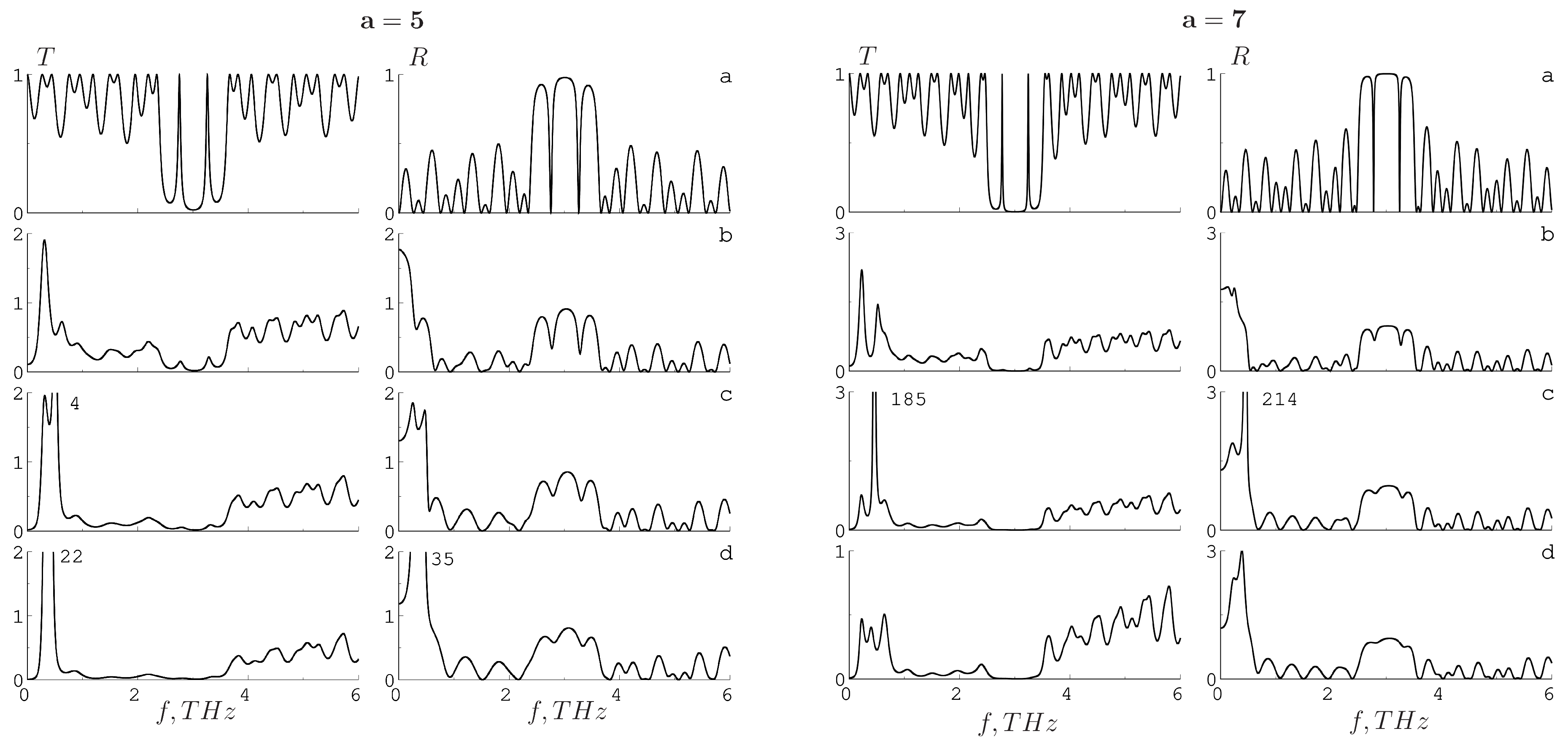
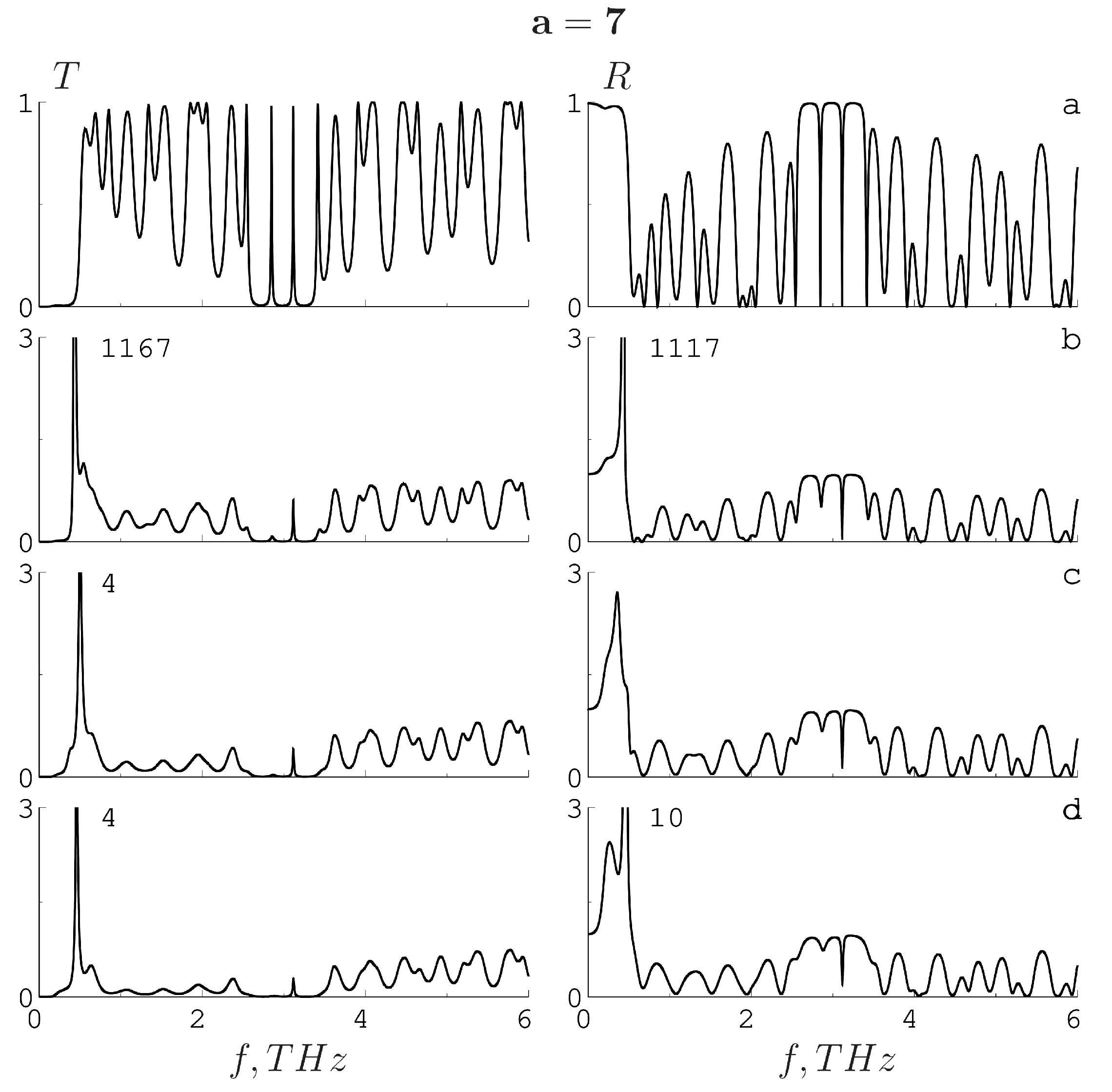
Figure 5 shows the transmission and reflection spectra for an MCR with a number of periods in the BMs
and a resonator cavity filled with a “semiconductor/graphene” structure with a transfer matrix
. The material of the semiconductor layers is n-InSb (its parameters are given in the description of
Figure 3). The spectra are plotted for the Fermi energies
= 0, 100, 200, 300 meV (a–d) in the absence of a magnetic field (
). The semiconductor used as barrier layers is a material with free charge carriers and with a higher permittivity value than
, partially modifying the spectra compared to those presented in
Figure 4b. Thus, in the considered MCR structure in the low-frequency region of the spectrum (below the plasma frequency), a region of almost complete non-transmission appears; there is a narrowing of the PBG and a complete suppression of the low-frequency and incomplete suppression of the high-frequency defective modes at
; the maximum amplification in the region
turns out to be significantly higher than when the cavity is filled with the “graphene/dielectric” structure.
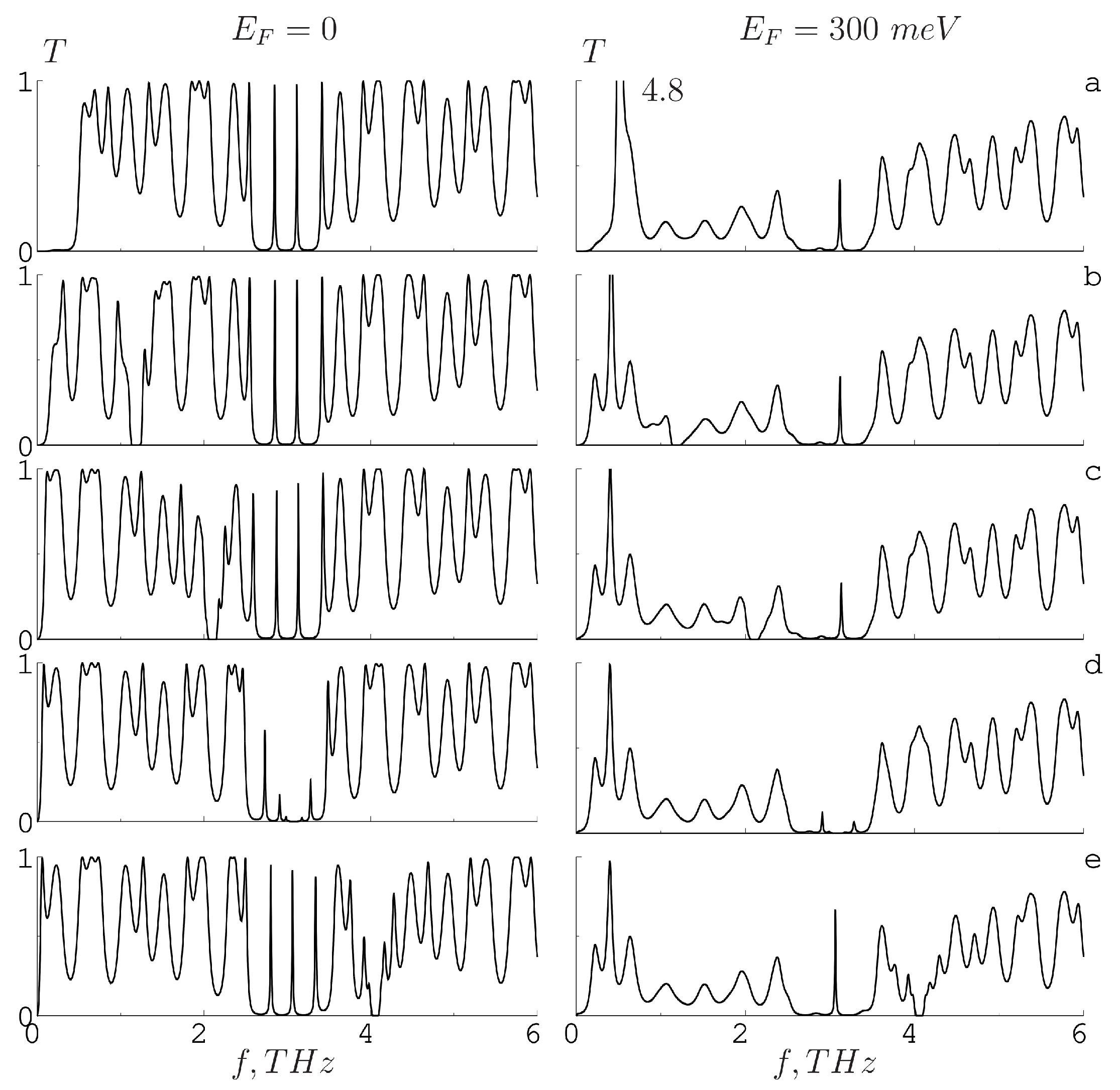
Figure 6 shows the transmission spectra of the same structure; however, with the value of the control parameters
= 0, 300 meV (graphs left, right) and
= 0, 5, 10, 15, 20 kOe (a–e). It can be seen that, for a MCR structure with unexcited graphene layers
, the value
does not exceed unity for all values of the magnetic field. It seems interesting that the width of the PBG increases with an increasing magnetic field due to the splitting of narrow lines from the gap boundaries. The amplification of the transmission spectra takes place for a microcavity structure with
in the region of negativity of the real part of the conductivity (
THz), i.e., in the region
THz, the coefficients
become greater than unity. In this case, the suppression of the transmission lines is observed inside the PBG. The influence of the magnetic field affects the spectra by suppressing a narrow section corresponding to each field value in the position of the cyclotron resonance line (see
Figure 3). As
increases, the transmission suppression region shifts towards higher frequencies.
4. Discussion
In the region of a weak external electric field
, the specific conductivity of the semiconductor does not depend on
, while at higher values of
, an exponential increase in the specific conductivity begins. The boundary value of the electric field strength between the region of weak and strong fields is called critical, the estimate of which is given by the expression
, where
ℓ is the mean free path of an electron and
is the Boltzmann constant. If we take
K,
m, the value of the critical field
V/m. Thus, at
, we can consider the specific conductivity and consequently, the dielectric constant of the semiconductor to be independent of the strength of the external electric field. The values
used in the work are determined by the chemical potential
(Fermi energy
) of the graphene monolayer. The dependence of the chemical potential of graphene on the external field
is determined by the expression [
19,
20]:
where
is the Fermi–Dirac distribution,
is the energy of the electron, the Fermi speed is
= 10
m/s and
is the permittivity of the substrate.
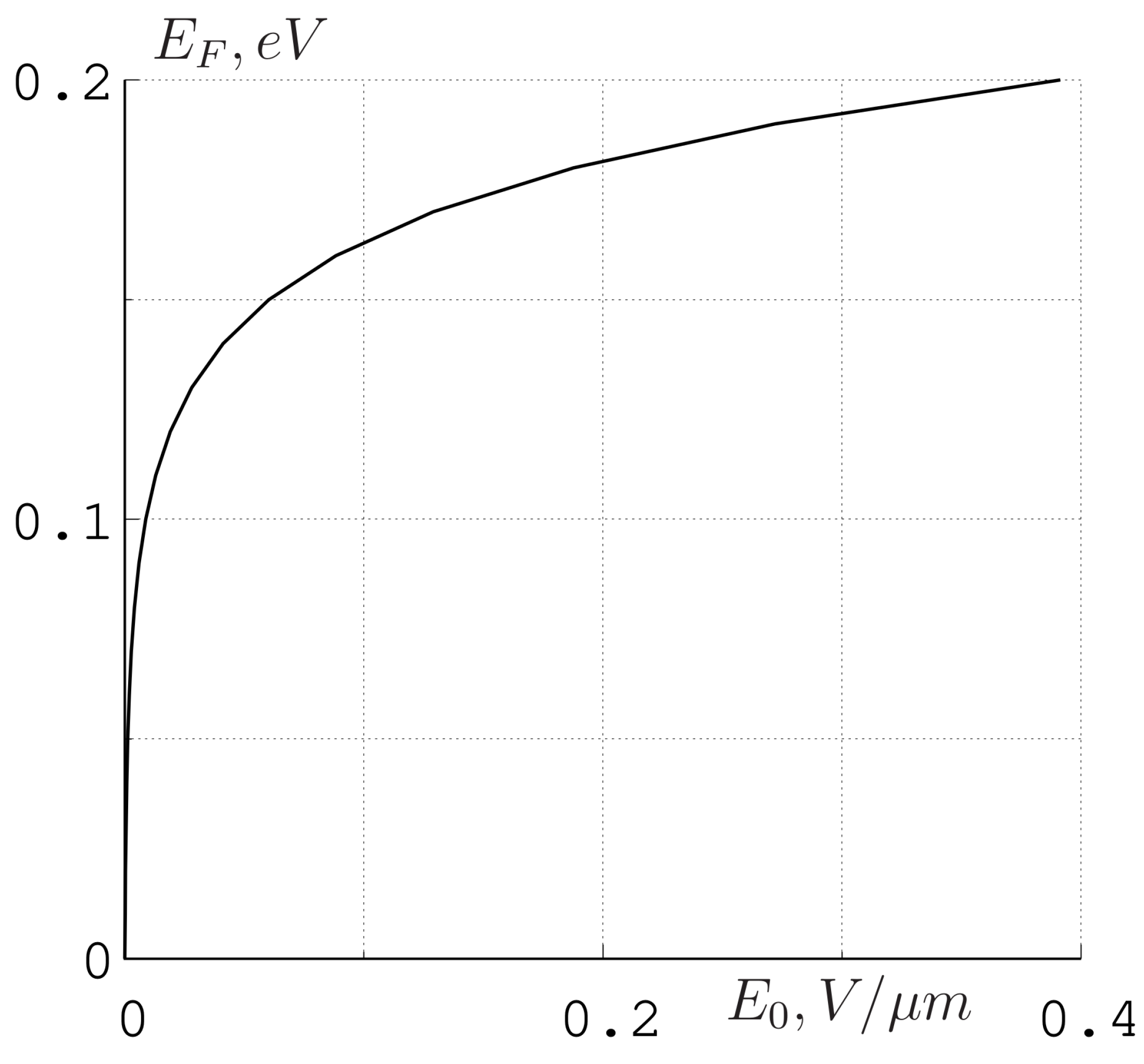
Figure 7 shows the dependence of the chemical potential of graphene on the electric field strength for the permittivity of the substrate
, obtained on the basis of (
6). It follows from the above dependence that, for the used values of the chemical potential, the strength values
vary within (10
–10
) V/m, which can be attributed to the region of weak fields. The influence of a magnetic field on the properties of a semiconductor is taken into account by the resonant dependence (
4) of the components of its permittivity on the magnetic field strength, which enters into the expression for the cyclotron frequency. The magnetic field applied in the plane of the graphene layers (namely that such a configuration is considered in the work) has no effect due to their transverse monoatomicity.
5. Conclusions
This paper presents the frequency dependencies of the transmission and reflection coefficients for a wave propagating in a symmetric MCR structure with dielectric BMs. The active layer, which is a periodic graphene-containing structure with the controlled material parameters of individual layers, completely fills the working cavity of the resonator. When the cavity is filled with a structure with quantum wells (graphene monolayers), a regime of strong exciton–photon interaction between the defective cavity mode and quantum well excitons is realized. This leads to the splitting of the exciton and photon levels into two polariton states and to a significant transformation of the transmission and reflection spectra.
It is shown that the transformation of the spectra in an MCR with the “dielectric/graphene” structure occurs due to a change in the conductivity of the graphene monolayers when their Fermi energy changes under the action of an external electric field, and in an MCR with the “semiconductor/graphene” structure, it also occurs due to a change in the permittivity of the semiconductor layers when exposed to the external magnetic field. The conductivity real part of the graphene layers, through which a direct electric current flows, can become negative in the range 2 THz, which leads to terahertz radiation amplification in a structure with graphene layers at the charge carrier drift velocities lower than the phase velocity of an electromagnetic wave. In the frequency range 0.5 THz, when modeling photon spectra, the method of transfer matrices was used to describe the optical properties of the BMs and the active layer. Numerical results show that the transmission and reflection spectra in the studied terahertz region can be effectively controlled and transformed both due to a change in the Fermi energy of graphene monolayers by an external electric field, and as a result of a change in an external magnetic field.
Such an MCR structure can find wide practical application, in particular, it can serve as an effective filter in the narrow frequency region of the defect mode, as well as a polarizer in the region where a wave of only one polarization is transmitted. The operating frequency range of the MCR can be changed over a fairly wide range by choosing the material of the layers, their thickness, the type and concentration of carriers, as well as by choosing the period of the BMs.


