1. Introduction
Additive manufacturing technologies such as 3D printing have been widely used in the fabrication of complex objects at low cost. Recently, the application of these technologies has been extended to the fabrication of metamaterials and metasurfaces, which are capable to modify the propagation of electromagnetic waves. These structures can be used to improve beam directivity, generate Gaussian and Bessel beams, increase antenna gain, and improve signal-to-noise ratio [
1,
2,
3,
4,
5,
6,
7].
Metasurfaces are artificial structures that are designed to modulate the propagation of electromagnetic waves at various frequencies. They are composed of a series of subwavelength elements that can be 3D printed using metal or thermoplastic, milled, and cut [
8,
9], making their fabrication relatively simple and inexpensive. Metasurfaces have numerous applications, such as for flat-focusing lenses [
7,
10], frequency-selective filters [
11], reflectors [
12], polarizers [
13], and broadband absorbers [
14].
One of the most promising applications of metasurfaces is in the field of telecommunications, specifically in 5G. With the increasing demand for higher data rates and wider network coverage, metasurfaces have the potential to significantly improve antenna efficiency and therefore, signal quality [
15,
16,
17]. Moreover, intelligent metasurfaces are a rapidly growing area, with applications in areas such as encryption [
18], mind–machine interfacing [
19], and diffractive computing [
20]. However, characterizing the spatially varying profile generated by both 5G-specific and intelligent metasurfaces is a significant challenge.
In this context, we present a low-cost instrument for the multidimensional characterization of advanced wireless communication devices, fully automated with four axes and capable of collecting more than 1.6 million measures of X–Y axis sweeping, translating in the Z axis, with approximately 5 µm of precision and rotating 360° with 1.8° of resolution for full image reconstruction and structure characterization. This paper also validates the suitability of this low-cost instrument by characterizing and verifying (with simulation results) a known component, e.g., a previously fabricated metasurface. It must be noted that surprisingly, neither automated instruments for microwave characterization nor metasurface characterization and image reconstruction are currently available in the literature. Usually, such experiments use a somewhat archaic and manual setup, making the device characterization process not only tiresome, but also error prone.
This paper is organized as fallows:
Section 2 presents the system overview, detailing its main components;
Section 3 reveals the details of the instrument hardware;
Section 4 describes the hardware integration;
Section 5 depicts a graphical user interface developed to control the instrument and the performance in terms of time, accuracy, and resolution;
Section 6 presents an application of the instrument, characterizing a 30 GHz metalens, and providing the results and a discussion, and
Section 7 presents the conclusions.
2. System Overview
All components of our instrument were primarily designed and constructed using 3D CAD software, specifically Autodesk Fusion 360 Academic License. These components were then fabricated using a GLC-1490 laser cutter from Glorystar Laser Technology Company and a GTMax 3D Core A1 3D printer, using acrylic and ABS materials, respectively. The instrument parts were assembled with different sizes of M3 screws and nuts.
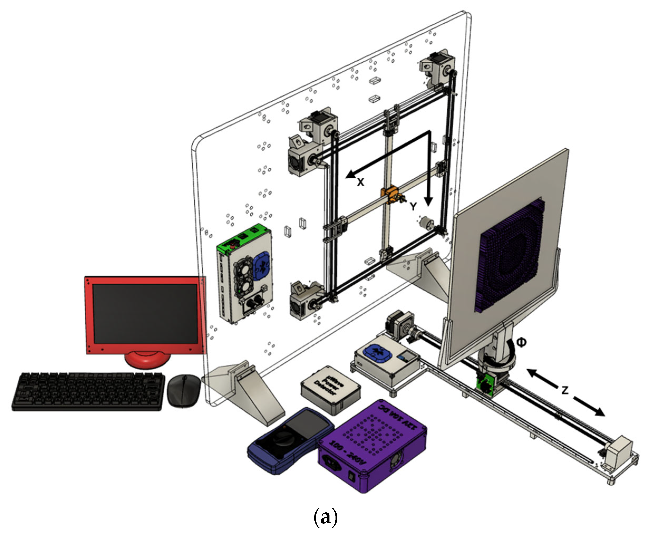
Figure 1a depicts the 3D design of the instrument, while
Figure 1b displays a photograph of the fully assembled instrument.
We used a Rohde & Schwarz (R&D) ZVA-40 vector network analyzer (VNA) as a signal generator and produced a signal with a power of +15 dBm and a frequency of 30 GHz. This equipment has the capability to produce signals within the frequency range of 10 MHz to 40 GHz. The signal power varies based on frequency, with the typical signal power range for frequencies of 20 GHz to 32 GHz being −40 dBm to +15 dBm [
21]. The signal was transmitted using a WR-34 horn antenna from Pasternack, which has a nominal gain of 20 dBi and a 17° (17.4°) vertical (horizontal) half-power beamwidth (HPBW) [
22]. A schematic representation of the system overview utilized to characterize metasurfaces using the instrument described in
Figure 1 is shown in
Figure 2.
After being transmitted by the metasurface, the signal is received by a helical antenna [
23]. This type of antenna was selected for the prototype due to its ease of design and fabrication and its reduced dimensions, which allow for a higher spatial resolution.
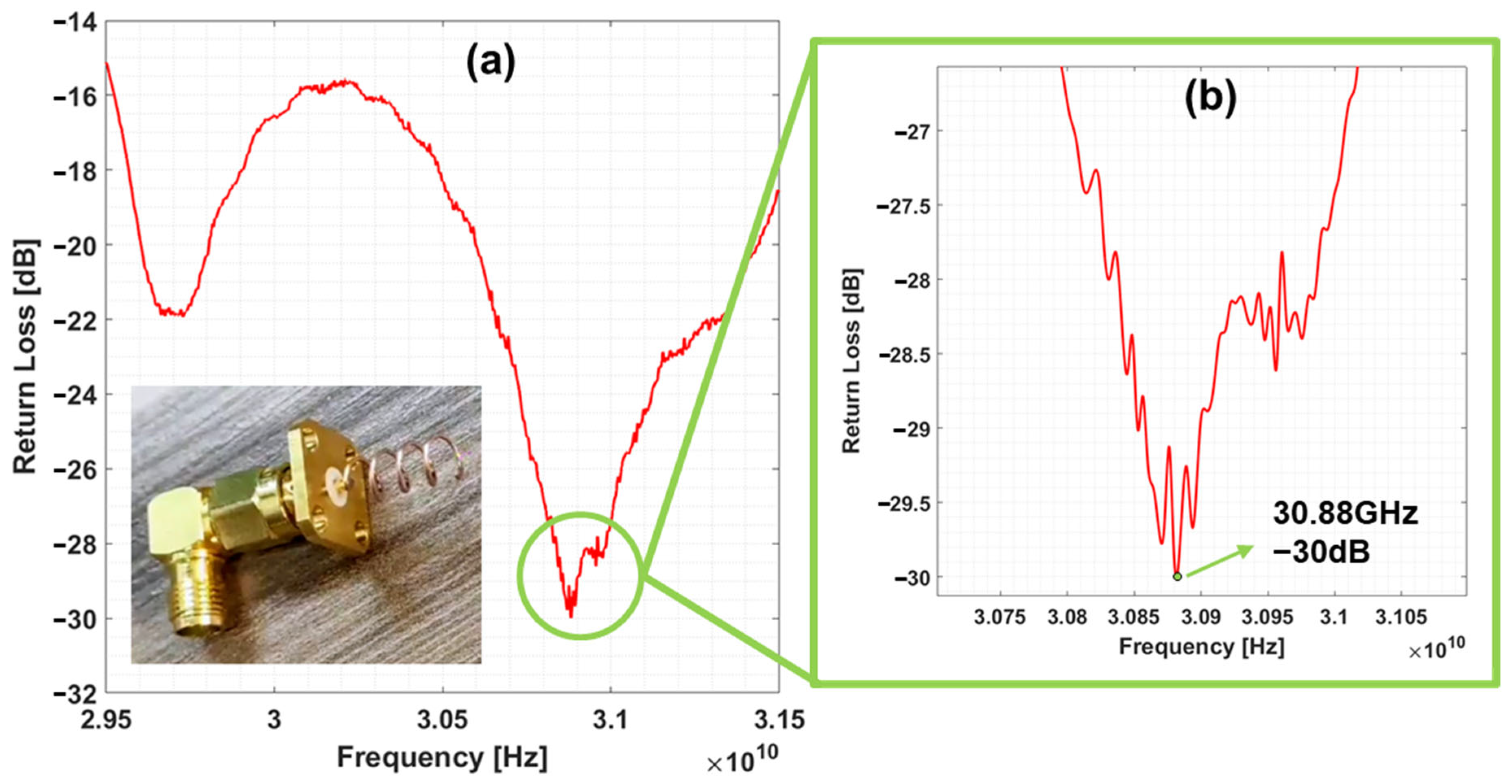
Figure 3 presents the design specifications for the helical antenna used in this research.
The fabricated antenna was designed to have low return loss at 30 GHz, with a length equal to the operating wavelength (10 mm), an inter-helix spacing (S) equal to λ/4, and a diameter (D) of 3.18 mm, as shown in
Figure 3. A photo of the antenna can be seen in the inset of
Figure 4a.
Figure 4a shows the measured return loss of the antenna as a function of the operating frequency obtained with the VNA. Note that the return loss minimum actually occurred at a slightly higher frequency of 30.88 GHz, as shown by
Figure 4b. This is probably due to small deviations in the fabricated antenna length.
3. Hardware
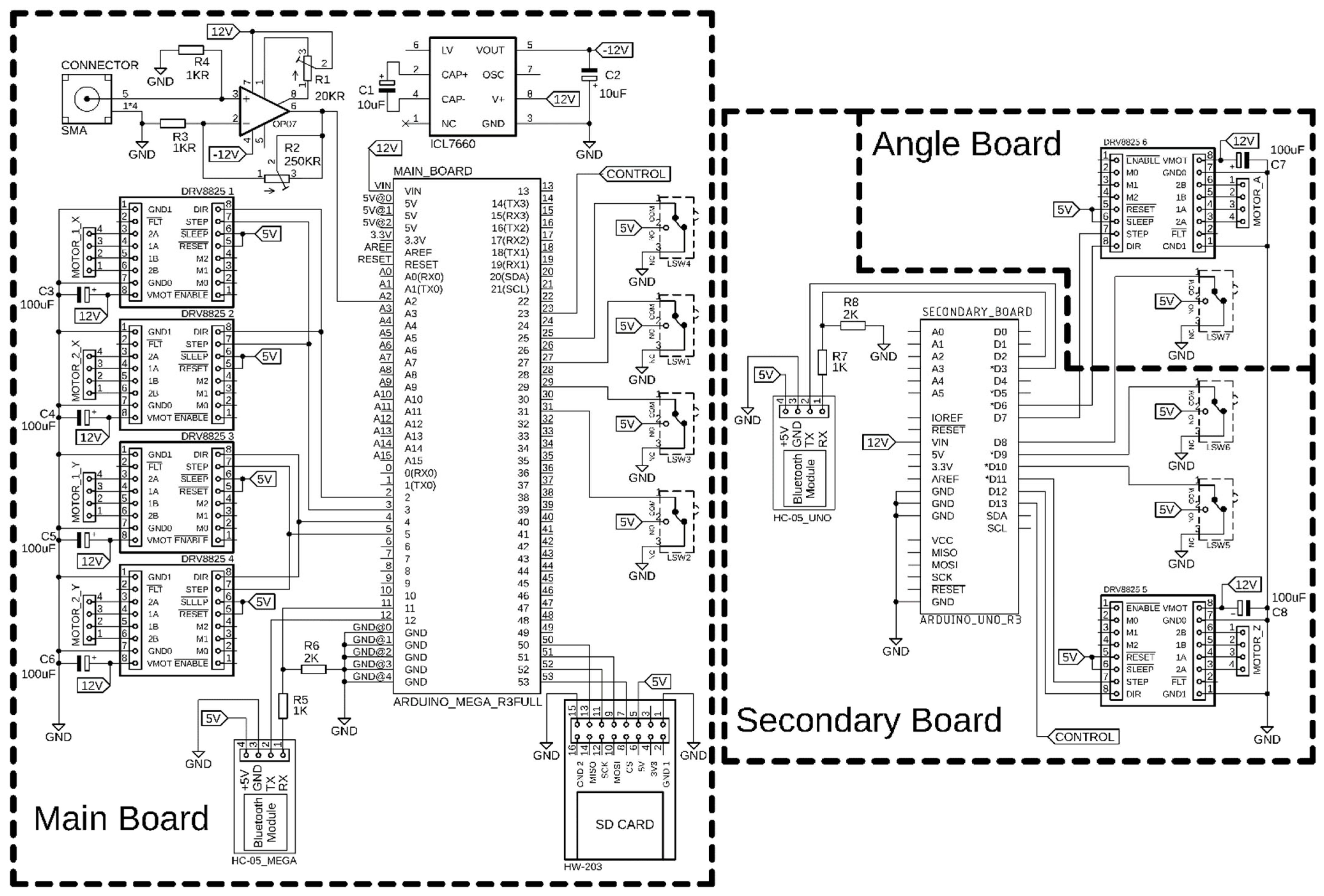
Figure 5 displays the hardware schematic of our assembled instrument, which consists of three printed circuit boards (PCBs) designed using Fusion 360 electronics design software. The PCBs were fabricated using the ProtoMat S103 PCB milling machine from LPKF Laser & Electronics. Additional files are available in the
Supplementary Materials.
The main board is equipped with an Arduino Mega 2560, which serves as the primary controller for the instrument. The Arduino Mega 2560 is a microcontroller-based board which has 54 digital input/output pins, 15 of which can be used as PWM outputs, 16 analog inputs, 4 UARTs (hardware serial ports), a 16 MHz crystal oscillator, a USB connection, a power connector, an ICSP connector, and a reset button. The microcontroller features 256 KB of flash memory, 8 KB of which is occupied by the board’s bootloader, 8 KB of SRAM memory, and 4 KB of EEPROM memory.
The secondary board features an, which is responsible for controlling the Z-axis translation and angle board rotation of the characterized metasurface in the instrument. The Arduino Uno is a microcontroller-based board with 14 digital input/output pins, 6 of which can be used as PWM outputs, 6 analog inputs, a 16 MHz ceramic resonator, a USB connection, a power connector, an ICSP connector, and a reset button. The microcontroller has 32 KB of Flash memory, 0.5 KB of which is occupied by the board’s bootloader, 2 KB of SRAM memory, and 1 KB of EEPROM memory.
The receiver antenna can move on the XY plane, whereas the metasurface can move in the
Z direction and rotate along the
Z axis, as can be seen in
Figure 1a. Each of these degrees of freedom is actuated by a Nema 17 HS4401 stepper motor that is driven by a DRV8825 driver. The translation is aided by a threaded shaft. Each stepper motor has a torque of 0.42 N∙m uses up to 1.7 A per phase, and has a resolution of 1.8° per step, with 200 steps per turn. The motors measure 42 × 42 × 40 mm and weigh 280 g. The DRV8825 features an adjustable SMD potentiometer for current limiting, overcurrent and overtemperature protection, and the ability to operate with up to six microstep resolutions (1, 1/2, 1/4, 1/8, 1/16, and 1/32 step). It operates from 8.2 V to 45 V and can deliver up to approximately 1.5 A per phase, without a heat sink or forced airflow. With proper heat dissipation, this driver can reach up to 2.2 A per coil.
The data collected is stored on a SD card using an SD card module HW-203 installed on the main board. The received RF signal is directed to a LTC5596 RMS power detector, which is mounted on a DC2158A evaluation board, from analog devices. The LTC5596 is a high-precision power detector that offers a wide RF input bandwidth from 100 MHz to 40 GHz, with a linear response in dB and a logarithmic slope of 29 mV/dB over a dynamic range of 35 dB, with accuracy typically better than ±1 dB. Note that in our setup, the frequency response of the helix antenna (see
Figure 4) is sufficient to filter out any other signal that is present in the environment. In the case of a noisy environment or when using broadband antennas, an RF filter stage can be added prior to the LTC5596 to assure that only the frequency of interest is being detected.
Figure 6 illustrates the instrument’s signal conversion system, which includes a 3D-printed case to shelter the components, connectors, and a power switch (a), a DC2158A evaluation board for LTC5596 IC and a voltage regulator circuit to convert 12 V in 3.3 V (b), and the zoomed-in image of DC2158A showing LTC5596 IC, RF in, and DC out (c).
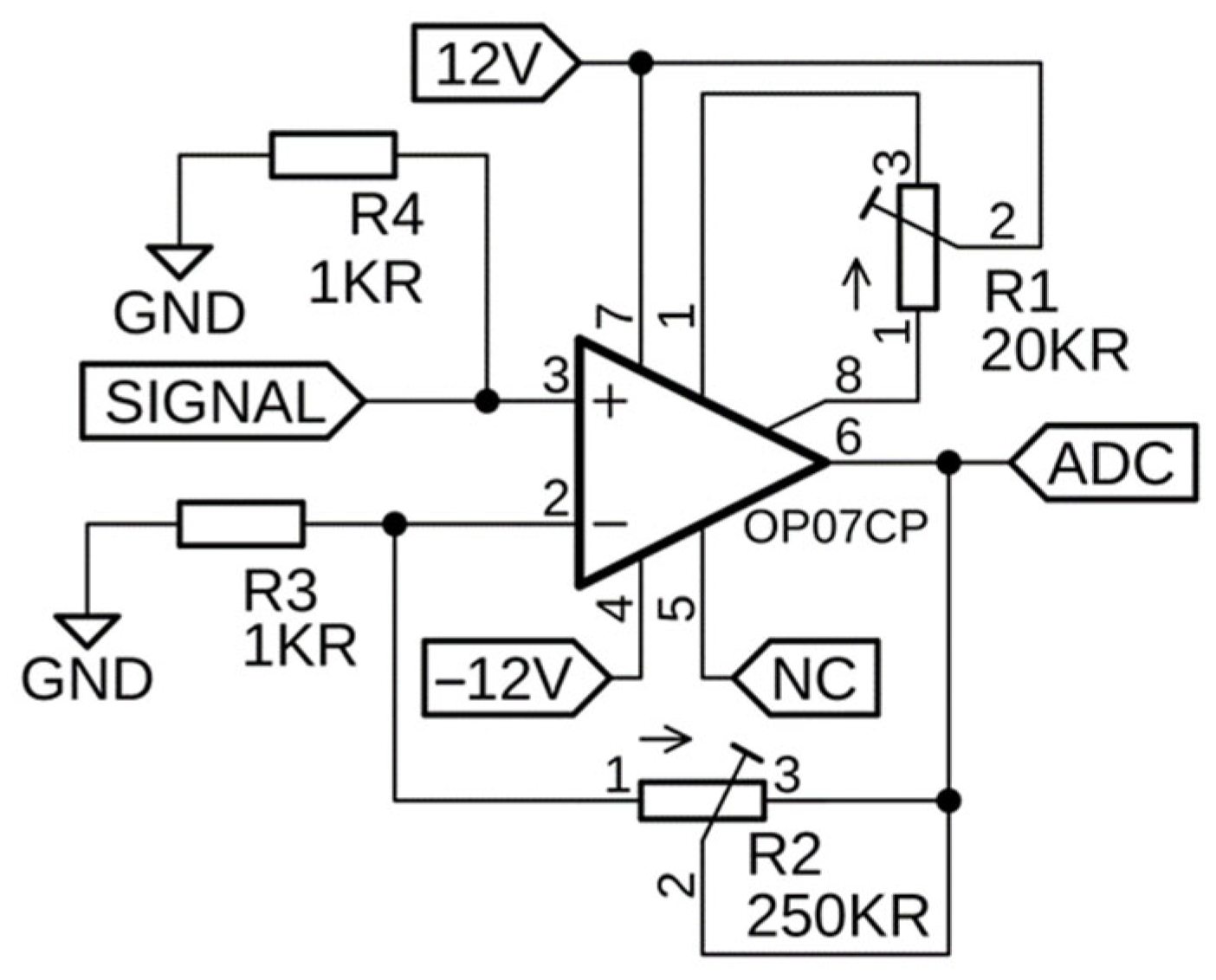
Following the DC conversion, the signal is directed to an operational amplifier (OP07) integrated within the main board of the instrument. The OP07 operates with a very low input offset voltage of 75μV, achieved by the trimming of the wafer stage, which eliminates the requirement for suppression by external components, in most cases. Additionally, the OP07 features a low input bias current of ±4 nA and a high open-loop gain of 200 V/mV. This combination of high open-loop gain and low offset voltage make the OP07 particularly useful for high-gain instrumentation applications. The amplifier was installed in a non-inverting configuration, as the power detector delivers a positive DC voltage. The OP07 negative feedback is provided by an ICL7660, which converts the supply voltage from positive to negative over an input range of 1.5 V to 12 V, resulting in complementary output voltages from −1.5 V to −12 V. Our instrument has been designed to accommodate a wide range of applications; thus, the amplifier gain is configurable.
Figure 7 illustrates that the amplifier gain can be modified according to the operator’s needs through the use of a 250 KΩ potentiometer (R2) and a 1 KΩ precision resistor (R3). Furthermore, R1, another potentiometer, is utilized for offset nulling, as described in [
24].
The instrument’s main and secondary controls communicate with a graphical user interface (GUI) developed on a Raspberry Pi 4 to receive initial measurement parameters, pause the measurement, or reset the microcontrollers to restart. This communication is facilitated through Bluetooth, using two HC-05 Bluetooth modules installed on the main control and secondary control shields. The HC-05 is a class 2 Bluetooth module with a serial port profile, capable of being configured as either a master or slave. The Bluetooth communication protocol used is v2.0+EDR, with a 2.4 GHz frequency in the ISM band and GFSK modulation.
4. Hardware Integration
The microcontroller on the instrument main board controls the movement of the stepper motors by sending direction and step signals to four DRV8825 drivers, which are also installed on the main board. These signals then drive the four Nema 17 motors, enabling movement on the X (horizontal) and Y (vertical) axes. Two motors are controlled by a step and direction signal for movement on the X axis, and the other two motors are controlled by a separate step and direction signal for movement on the Y axis, all while adhering to the parameters received via Bluetooth from the GUI running on a Raspberry Pi 4.
Data acquisition is primarily performed by the receiving antenna, which directs the signal through a Thorlabs RF cable model KMM36 to the LTC5596 power detector board. This board converts the RF signal into a DC signal, which is then sent to the OP07 operational amplifier on the main board’s shield. The analog input of the Arduino Mega microcontroller reads the DC signal and stores it on an SD card in matrix form. The antenna begins the measurement in the upper right corner of the instrument and moves from right to left, collecting data as configured in the GUI. After reaching the end of the course, it moves down and back from left to right, collecting more data until it reaches the bottom of the instrument. Finally, the antenna returns to the starting point in the upper left corner.
Upon completion of the matrix data collection, the Arduino Mega sends a control signal to the Arduino Uno on the secondary shield, which controls two Nema 17 motors to perform the
Z axis translation and rotation movement of the metasurface being characterized. After the
Z axis translation movement or rotation is complete, the Arduino Uno sends a control signal back to the Arduino Mega, and the process repeats.
Figure 8a shows the front of the main board cover case, with the fans to cool down the motor drivers and potentiometers to adjust the operational amplifier offset and gain; (b) shows the back of main board cover case, with the HC-05 Bluetooth module fixed; (c) shows the main board with the mounted Arduino Mega 2560,
X and
Y axis DRV8825 motor drivers, ICL7660 voltage converter, OP07 operational amplifier, and the HW-203 SD card module; (d) shows the front of the secondary board cover case, with a 3D-printed Bluetooth symbol that fixes the HC-05 Bluetooth module in the back of cover case (as well as for the main board case); (e) shows the secondary board with the mounted Arduino Uno and
Z axis DRV8825 motor driver; (f) shows the back of the secondary cover case, with the HC-05 Bluetooth module fixed; and (g) shows the angle board with the DRV8825 motor driver responsible for supplying and controlling the metasurface rotation stepper motor.
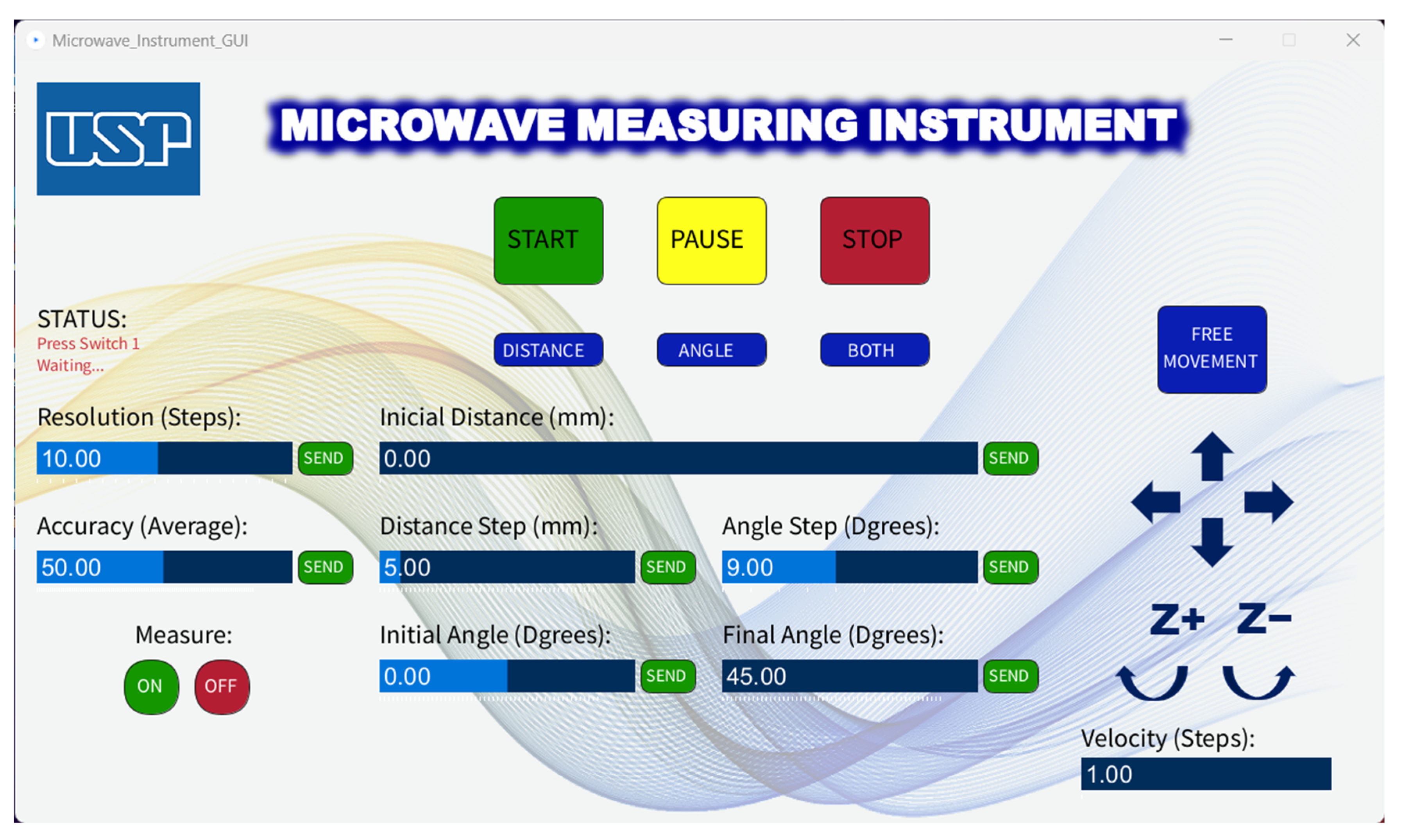
5. Graphical User Interface (GUI)
We used the Processing Development Environment, which is an open-source programming language, and the Integrated Development Environment (IDE) to develop an instrument graphical user interface (GUI).
Figure 9 depicts the GUI screen running on the Raspberry Pi 4.
At the top of the GUI, there are three buttons:—START, PAUSE, and STOP—as depicted in
Figure 9. The START button has multiple functions, primarily to activate the instrument. This button is used to trigger the start signal to the Arduino Mega Microcontroller, to advance the OP07 operational amplifier gain configuration, and to resume measurements if the PAUSE button has been pressed. The PAUSE button is used to pause the motors and measurement collection, and the instrument remains paused until either the START or STOP button is pressed. The STOP button resets the microcontrollers, sending a reset command and restarting the entire characterization process.
The sequence of actions to be taken on the GUI to configure the instrument parameters is displayed to the operator as a text message in the “STATUS” field, located below and to the left of the START, PAUSE, and STOP buttons, as shown in
Figure 9.
After configuring the operational amplifier gain and offset, it is necessary to define the resolution of the matrix data to be collected. This is done through the RESOLUTION slider, which sets the number of steps that the motors will rotate in each measurement. The operator sets the slider position and then clicks the SEND button next to the slider. A smaller number of steps results in a higher resolution matrix, with the time to complete a measurement being inversely proportional to the square of the resolution. The highest configurable resolution is 1 step, which corresponds to a matrix with 1200 × 1200 pixels, and the lowest resolution is 20 steps, which corresponds to a matrix with 60 × 60 pixels, as shown in
Figure 10.
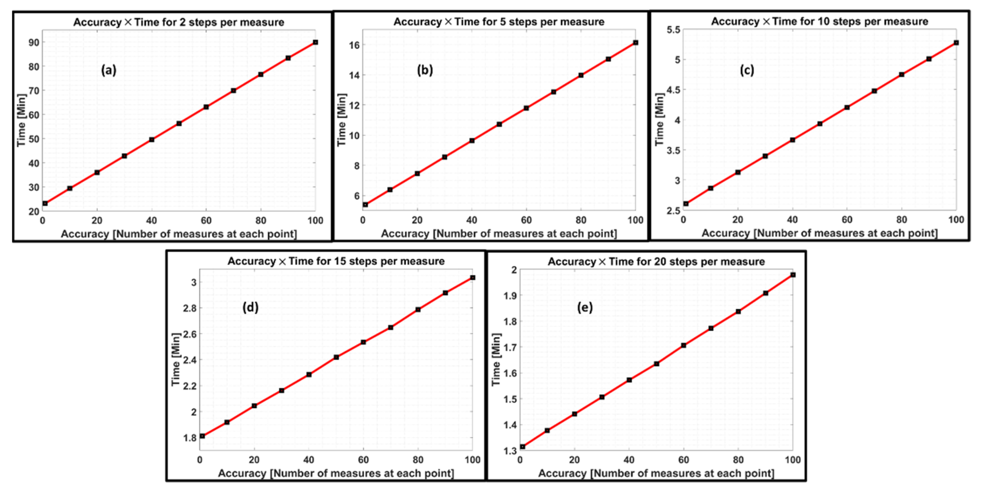
The average of N (1 ≤ N ≤ 100) measurements stored per pixel is used to increase the signal-to-noise ratio of the measurement. This property is adjusted with the help of the ACCURACY slide on the GUI. It is important to note that a higher accuracy will result in a longer time for the instrument to complete a measurement matrix, following a linear trend, as can be seen in
Figure 11.
Once the accuracy and resolution settings are set, the instrument will position the receiving antenna at the starting point of the measurements, and the operator must then choose the type of characterization to be performed.
Figure 9 depicts three buttons on the GUI: DISTANCE, ANGLE, and BOTH. The DISTANCE option is used when the operator wants to execute measurements by only varying the distance between the metasurface and the receiving antenna. The ANGLE button is used to perform measurements by only varying the angle between the metasurface and the receiving antenna, with a fixed distance. The BOTH option is used to execute measurements by both varying the angle and distance between the metasurface and the receiving antenna, first the angle variation and then the translation in the
Z axis.
The operator must first specify the initial parameters for the distance between the metasurface and the receiving antenna by adjusting the value of the DISTANCE slider. This value determines the starting point of the measurements. If the operator selects either the DISTANCE or BOTH characterization option, it is mandatory to provide information regarding the object’s movement in the Z-axis during each measurement cycle, which must always be away from the receiving antenna. This is achieved by adjusting the DISTANCE STEP slider.
The subsequent step involves setting the angle parameters between the metasurface and the receiving antenna. The operator first specifies the initial angle by adjusting the value of the INITIAL ANGLE slider, within a range of −45° to 45°, with 0° being the point at which the metasurface is perpendicular to the receiving antenna. The operator then sets the final angle for the measurements by adjusting the FINAL ANGLE slider. It is important to note that the difference between the absolute value of the initial and final angles must always be greater than the value set in the ANGLE STEP slider. If the FINAL ANGLE and ANGLE STEP sliders are configured to values that are not permissible, the GUI will display an error message and block the SEND buttons for these two settings.
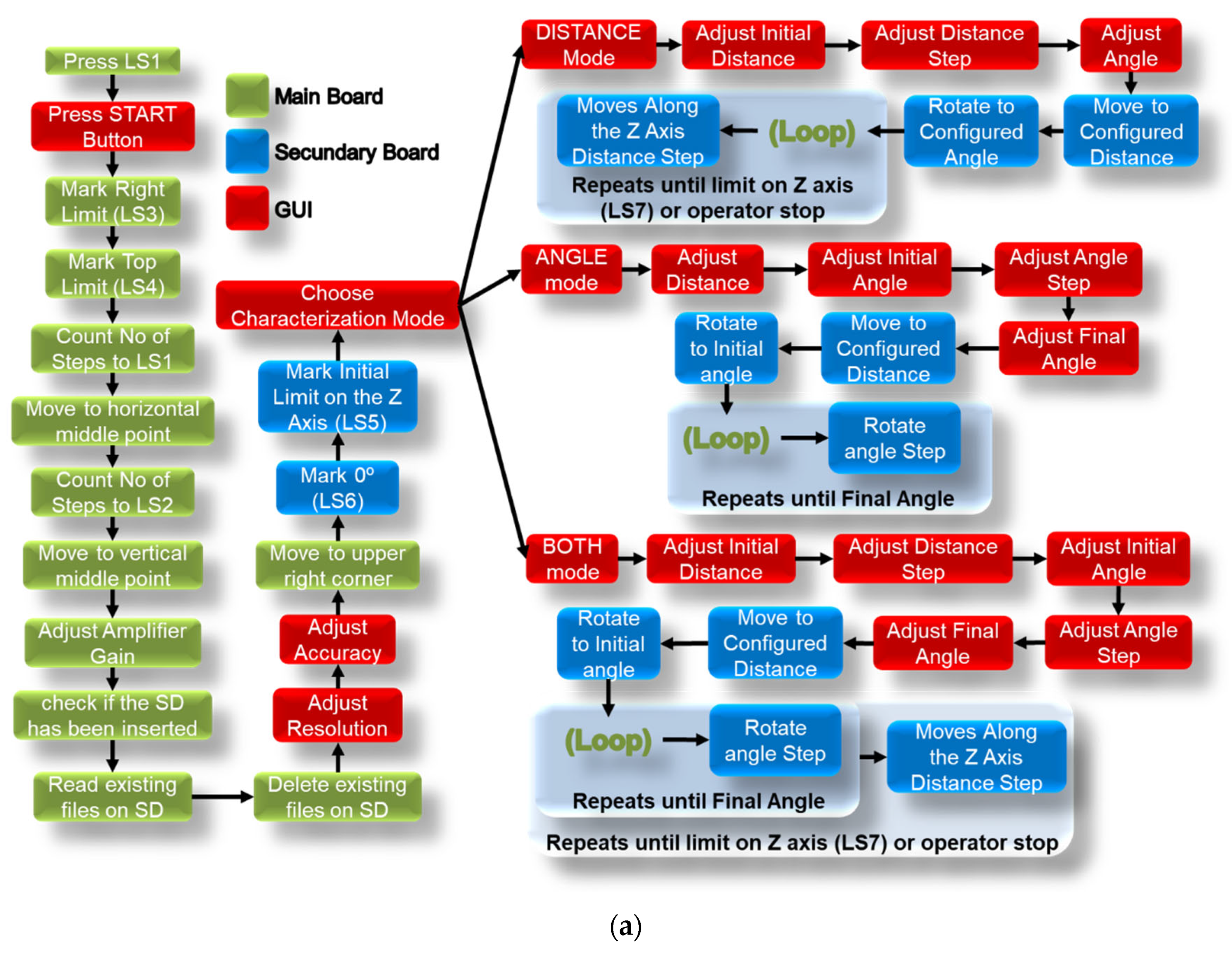
Figure 12 depicts the system operation. Functions performed by the microcontroller of the main board (Mega) are represented in green, functions performed by the secondary board (Uno) are represented in blue, and functions performed in the GUI (Raspberry Pi 4), in which the operator performs the equipment configurations, are represented in red.
Figure 12b is the loop part (in green) that appears in
Figure 12a within the three modes of equipment operation. They are separated to provide a clearer demonstration of how the instrument operates.
6. Results and Discussion
In order to assess the practical utility of our equipment, the device was employed in the characterization of a 3D-printed metalens, fabricated with thermoplastic polylactic acid (PLA). The PLA plastic microwave permittivity was extracted according to the methods used in [
25]. The results obtained from the instrument were then compared to those obtained from computer simulations.
The metalens design used a hyperbolic phase profile with a 20 cm focal length, adjusted to operate at 30 GHz [
26]. It has a square area with sides measuring 15 cm. The phase control is made with 3D printed prisms with varying side lengths, which act as truncated waveguides [
7,
27]. The unit cell size is 6 mm, and the posts are 18 mm tall. The phase profile was sampled using eight phase levels, which required the same amount of different structures in the design. More details can be found in [
7].
Figure 13 illustrates the fabrication processes involved in metalens manufacturing.
First, we simulated the metalens transmitted fields using the scalar angular spectrum formalism method [
28] and using the local post approximation [
29].
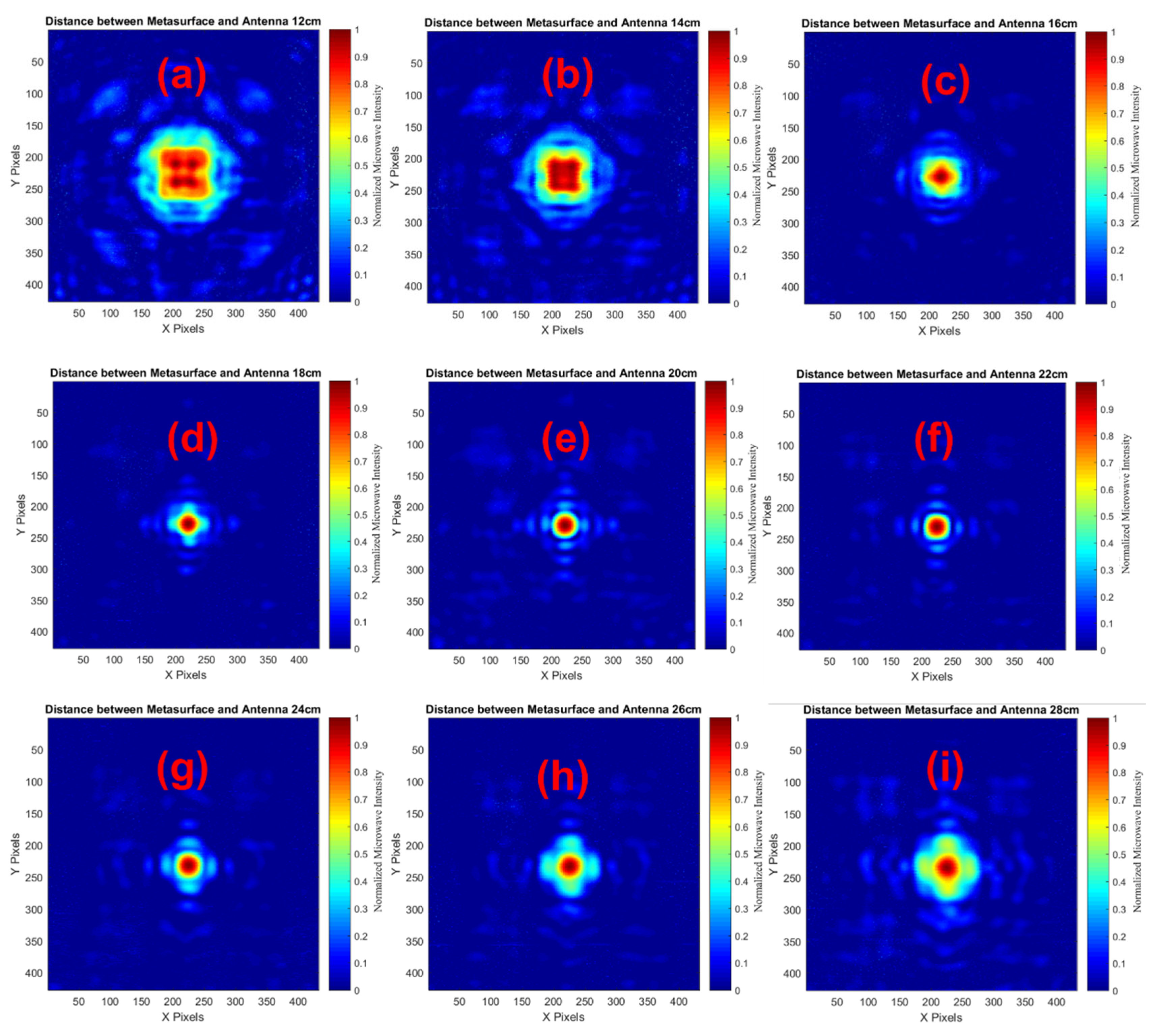
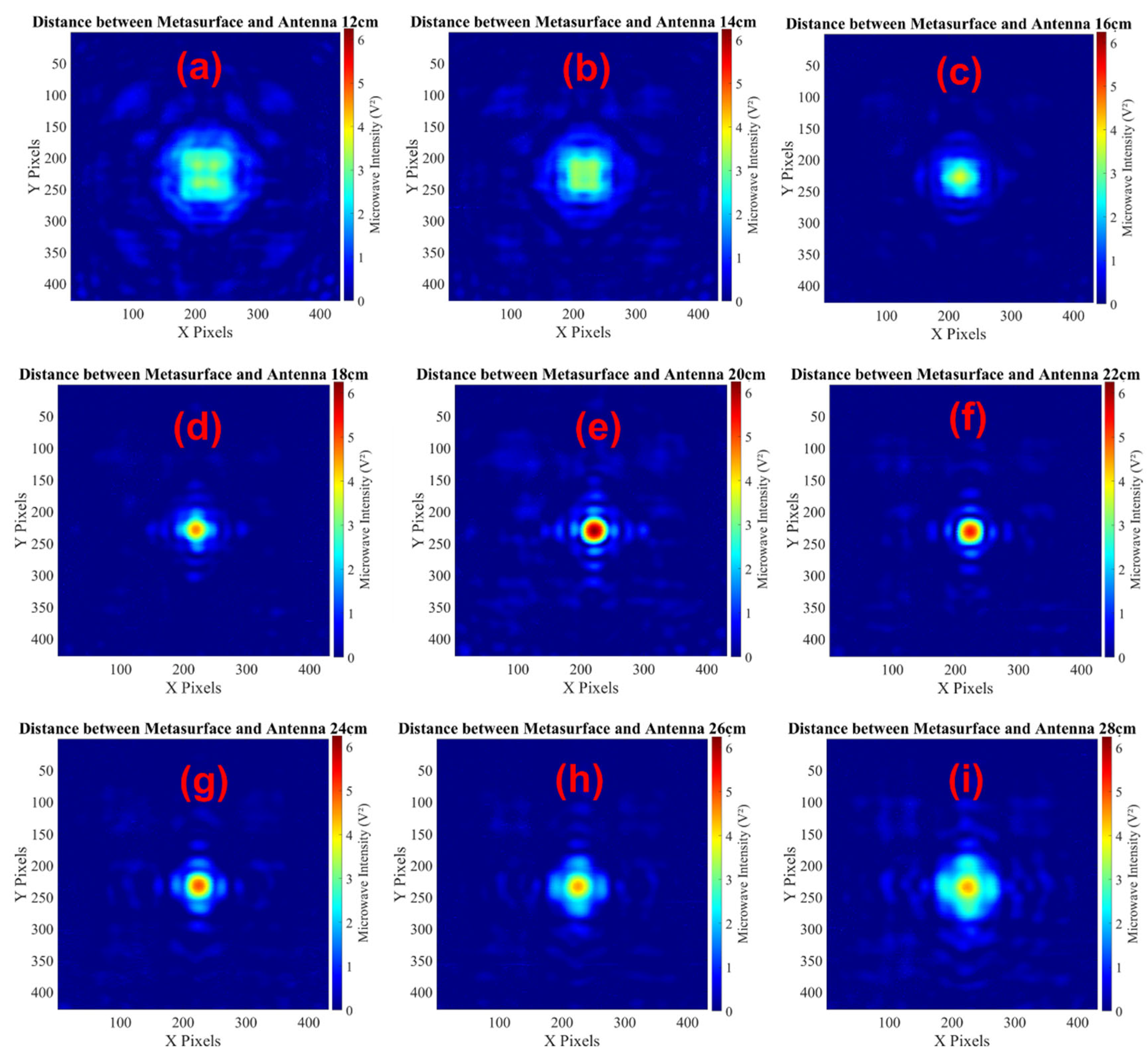
Figure 14 shows the normalized intensity distribution when increasing the distances from the metalens by 2 cm of increment, starting at 12 cm (
Figure 14a) and finishing at 28 cm (
Figure 14i). The intensity normalization in these reconstructions was performed considering the maximum and the minimum intensity of each distance matrix separately.
Figure 15 shows the normalized measured intensity distribution transmitted by the metalens, where (a–i) shows the intensity field at 12 cm to 28 cm, respectively, with steps of 2 cm. The intensity normalization was performed similar to the metalens simulation to maintain consistency in the comparison. These reconstructions provide a comprehensive view of the intensity distribution transmitted by the metalens at various distances from the receiving antenna, and they match quite well with the simulated intensity profiles shown in
Figure 14. The instrument GUI was configured with the following parameters to obtain the fields depicted in
Figure 15: a resolution of 3 steps per measurement and 50 measurements (accuracy) at each point. These settings resulted in the production of images with a size of 400 by 400 pixels. The good agreement between the simulation and the measurements highlights the high accuracy of the instrument and the quality of the fabricated metalens. This validation is crucial to ensure the accuracy and reliability of the results obtained from the use of the instrument for other future purposes.
Upon analysis of
Figure 14 and
Figure 15, a definitive determination of the actual focal length, previously stated as 20 cm, cannot be achieved. Thus, to establish the correspondence of the metalens behavior with the intended design,
Figure 16 exhibits the intensity fields, encompassing all the extracted measurements, where (a–i) shows the intensity field at a distance of 12 cm to 28 cm, respectively, with steps of 2 cm, similar to the images shown in
Figure 14 and
Figure 15.
Figure 16e exhibits conspicuously more intense measurements than the other figures, reaching a maximum intensity of 6.25 V
2, attesting to the consistency of the focal length with the originally intended specifications.
The instrument’s effectiveness has been demonstrated through the comparison of results obtained by measuring metalens intensity profiles with those obtained by computational simulation. This validation enables further exploration of the primary functionality of our developed instrument, which is the 3D reconstruction of the transmitted metalens intensity profile surface.
Figure 17 illustrates these measured reconstructions, showcasing the ability of the instrument to accurately measure the three-dimensional intensity profiles produced by the metalens. It was necessary to crop 1/4 of the 3D reconstruction in
Figure 17 to observe the innermost layers of the fields produced by the metalens. Note that the signal intensity increases as it approaches the focal length of the lens, reaching its maximum at 20 cm, which is the designed focal distance.
We used the previous measurements to characterize the metalens quantitatively with the 3 dB depth-of-focus (DOF) and the full width at half maximum (FWHM), located 20 cm away from receiving antenna.
Figure 18 presents the 3D reconstructions of the measured intensity surfaces until the 3 dB decay. Therefore, we measured an 11 cm 3 dB DOF and a 2.17 cm FWHM, as can be seen in
Figure 18a and
Figure 18b, respectively.
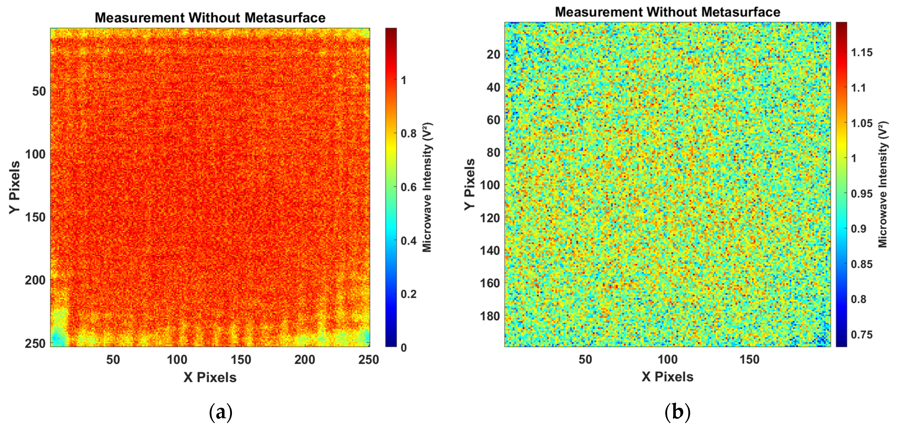
Thus, another parameter characterized and extracted from our manufactured metalens was the gain. A measurement cycle without the metalens positioned between the transmitting and receiving antennas was conducted to measure the signal intensity, without modulation from the metalens. The results can be seen in
Figure 19a.
It is noticeable that there is a pronounced signal oscillation at the edges of the matrix, caused by the presence of metal bearings, shafts, sensors, and motors at the edges. Therefore, it is appropriate to analyze the central part of the matrix shown in
Figure 19b, discarding the edges. To extract the gain of the metalens, it was necessary to compare the intensity measured by the instrument at the focal distance with the intensity measured when without a metalens between the antennas.
Figure 16e shows the matrix extracted at the focal distance, reaching a maximum intensity of 6.25 V
2. The average intensity collected in the scan without the metalens was 0.98 V
2, and comparing the two results, a ratio of 6.25/0.98 yields 6.38. Applying the logarithm: 10log(6.38) results in a gain of 8.05 dB.
7. Conclusions
In summary, we presented an innovative, low-cost instrument developed specifically for the precise characterization of microwave metasurfaces, particularly in the Ka band spectrum. This instrument is designed to offer an in-depth understanding of complex metasurfaces, such as a metalens, by allowing a thorough analysis of the point spread function in relation to the critical parameters. These include depth of focus (DOF), full width at half maximum (FWHM), and gain—quantified in our study as 11 cm, 2.17 cm, and 8.05 dB, respectively. This systematic characterization is pivotal for understanding the intricate design and functionality of metasurfaces.
A distinguishing feature of our proposed instrument is its capacity to generate data for 3D reconstruction of the metalens intensity distribution. This capability offers a comprehensive view of the metasurface properties, thus providing more robust analytical insights that go beyond conventional characterization methods.
The integration of these features in a single, cost-effective tool represents a significant advancement in the field of microwave metasurface characterization. With its broad application potential, this instrument promises to revolutionize metasurface investigations, opening new avenues for advancements in telecommunications and beyond.
Table 1 in our paper provides a detailed overview of the components of our instrument, itemizing each part, along with its respective cost, thereby demonstrating the affordability of our proposed tool. We believe this comprehensive cost breakdown will be beneficial for researchers aiming to replicate or build upon our design.
Overall, these findings and their consequent implications underscore the substantial value of our proposed instrument in enabling precise and comprehensive metasurface characterization across a myriad of potential applications.
Supplementary Materials
The following supporting information can be downloaded at:
https://www.mdpi.com/article/10.3390/app13116581/s1, The Supplementary Materials include all code files (instrument control firmwares and softwares), as well as all STL, DXF, and Gerber files to build the instrument. They can be downloaded at the article website.
Author Contributions
Conceptualization, R.G., A.M. and V.P.; methodology, R.G., A.M. and V.P.; software, R.G.; validation, R.G.; formal analysis, R.G.; investigation, R.G.; resources, R.G. and A.M.; data curation, R.G.; writing—original draft preparation, R.G.; writing—review and editing, R.G. and J.P.C.; visualization, R.G., B.-H.V.B. and J.P.C.; supervision, J.P.C.; project administration, J.P.C.; funding acquisition, B.-H.V.B. and J.P.C. All authors have read and agreed to the published version of the manuscript.
Funding
This research work was supported by the National Council for Scientific and Technological Development (CNPq), which is a foundation linked to the Ministry of Science and Technology (MCT) to support Brazilian research. The CNPq process number is 303562/2017-0. Rodrigo Gounella was supported by a Coordination for the Improvement of Higher Education Personnel (CAPES) scholarship, with process number: 88887.4829072020-00. Professor João Paulo Carmo was support by a PQ scholarship with the reference CNPq 304312/2020-7.
Institutional Review Board Statement
Not applicable.
Informed Consent Statement
Not applicable.
Data Availability Statement
Not applicable.
Acknowledgments
We would like to express our sincere gratitude to the Electrical and Computer Engineering Department (SEL) of the São Carlos School of Engineering (EESC) at the University of São Paulo (USP). We would also like to acknowledge the research funding agencies CNPq and CAPES for their support of this work.
Conflicts of Interest
The authors declare no conflict of interest. The funders had no role in the design of the study; in the collection, analyses, or interpretation of data; in the writing of the manuscript; or in the decision to publish the results.
References
- Shrestha, S.; Baba, A.A.; Abbas, S.M.; Asadnia, M.; Hashmi, R.M. A Horn Antenna Covered with a 3D-Printed Metasurface for Gain Enhancement. Electronics 2021, 10, 119. [Google Scholar] [CrossRef]
- Shrestha, S.; Zahra, H.; Abbasi, M.A.B.; Asadnia, M.; Abbas, S.M. Increasing the Directivity of Resonant Cavity Antennas with Nearfield Transformation Meta-Structure Realized with Stereolithograpy. Electronics 2021, 10, 333. [Google Scholar] [CrossRef]
- Liu, C.; Hu, C.; Wei, D.; Chen, M.; Shi, J.; Wang, H.; Xie, C.; Zhang, X. Generating Convergent Laguerre-Gaussian Beams Based on an Arrayed Convex Spiral Phaser Fabricated by 3D Printing. Micromachines 2020, 11, 771. [Google Scholar] [CrossRef] [PubMed]
- Gan, Y.; Meng, H.; Chen, Y.; Zhang, X.; Dou, W. Generation of Bessel Beams with 3D-Printed Lens. Int. J. RF Microw. Comput. -Aided Eng. 2020, 30, e22029. [Google Scholar] [CrossRef]
- Viskadourakis, Z.; Tamiolakis, E.; Tsilipakos, O.; Tasolamprou, A.C.; Economou, E.N.; Kenanakis, G. 3d-Printed Metasurface Units for Potential Energy Harvesting Applications at the 2.4 Ghz Frequency Band. Crystals 2021, 11, 1089. [Google Scholar] [CrossRef]
- Liu, Y.Q.; Sun, J.; Qi, K.; Che, Y.; Li, L.; Yin, H. High-Numerical-Aperture(NA) Microwave Metasurface Lens(Metalens) and Its Applications in High-Gain Antenna. In Proceedings of the 2021 19th International Conference on Optical Communications and Networks, ICOCN 2021, Qufu, China, 23–27 August 2021; Institute of Electrical and Electronics Engineers Inc.: Piscataway, NJ, USA, 2021. [Google Scholar]
- Pepino, V.M.; Da Mota, A.F.; Martins, A.; Borges, B.H.V. 3-D-Printed Dielectric Metasurfaces for Antenna Gain Improvement in the Ka-Band. IEEE Antennas Wirel. Propag. Lett. 2018, 17, 2133–2136. [Google Scholar] [CrossRef]
- Alex-Amor, A.; Palomares-Caballero, Á.; Molero, C. 3-D Metamaterials: Trends on Applied Designs, Computational Methods and Fabrication Techniques. Electronics 2022, 11, 410. [Google Scholar] [CrossRef]
- Bukhari, S.S.; Vardaxoglou, J.; Whittow, W. A Metasurfaces Review: Definitions and Applications. Appl. Sci. 2019, 9, 2727. [Google Scholar] [CrossRef]
- Kang, M.; Ra’Di, Y.; Farfan, D.; Alù, A. Efficient Focusing with Large Numerical Aperture Using a Hybrid Metalens. Phys. Rev. Appl. 2020, 13, 044016. [Google Scholar] [CrossRef]
- Jilani, S.F.; Falade, O.P.; Wildsmith, T.; Reip, P.; Alomainy, A. A 60-GHz Ultra-Thin and Flexible Metasurface for Frequency-Selective Wireless Applications. Appl. Sci. 2019, 9, 945. [Google Scholar] [CrossRef]
- Martínez-Llinàs, J.; Henry, C.; Andrén, D.; Verre, R.; Käll, M.; Tassin, P. A Gaussian Reflective Metasurface for Advanced Wavefront Manipulation. Opt Express 2019, 27, 21069. [Google Scholar] [CrossRef]
- Wang, X.; Wu, J.; Wang, R.; Li, L.; Jiang, Y. Reconstructing Polarization Multiplexing Terahertz Holographic Images with Transmissive Metasurface. Appl. Sci. 2023, 13, 2528. [Google Scholar] [CrossRef]
- Pung, A.J.; Goldflam, M.D.; Burckel, D.B.; Brener, I.; Sinclair, M.B.; Campione, S. Enhancing Absorption Bandwidth through Vertically Oriented Metamaterials. Appl. Sci. 2019, 9, 2223. [Google Scholar] [CrossRef]
- Tishchenko, A.; Ali, A.; Botham, P.; Burton, F.; Khalily, M.; Tafazolli, R. Reflective Metasurface for 5G MmWave Coverage Enhancement. In Proceedings of the 2022 International Symposium on Antennas and Propagation, ISAP 2022, Sydney, Australia, 31 October–3 November 2022; Institute of Electrical and Electronics Engineers Inc.: Piscataway, NJ, USA, 2022; pp. 507–508. [Google Scholar]
- Chen, Z.N.; Li, T.; Li, S.; Xue, C.; Lou, Q.; Liu, W.E.I. Microwave Metalens Antennas for 5G Network. In Proceedings of the 2021 15th European Conference on Antennas and Propagation (EuCAP), Dusseldorf, Germany, 22–26 March 2021. [Google Scholar]
- Rahamim, E.; Rotshild, D.; Abramovich, A. Performance Enhancement of Reconfigurable Metamaterial Reflector Antenna by Decreasing the Absorption of the Reflected Beam. Appl. Sci. 2021, 11, 8999. [Google Scholar] [CrossRef]
- Chen, L.; Ma, Q.; Luo, S.S.; Ye, F.J.; Cui, H.Y.; Cui, T.J. Touch-Programmable Metasurface for Various Electromagnetic Manipulations and Encryptions. Small 2022, 18, 2203871. [Google Scholar] [CrossRef] [PubMed]
- Luo, X. Directly Wireless Communication of Human Minds via Mind-Controlled Programming Metasurface. Light Sci. Appl. 2022, 11, 182. [Google Scholar] [CrossRef]
- Liu, C.; Ma, Q.; Luo, Z.J.; Hong, Q.R.; Xiao, Q.; Zhang, H.C.; Miao, L.; Yu, W.M.; Cheng, Q.; Li, L.; et al. A Programmable Diffractive Deep Neural Network Based on a Digital-Coding Metasurface Array. Nat. Electron. 2022, 5, 113–122. [Google Scholar] [CrossRef]
- Rohde & Schwarz R&S®ZVA Vector Network Analyzer Specifications. 2015.
- PE9851-2F-20; Pasternack WR-34 Standard Gain Antenna. Pasternack Inc.: Irvine, CA, USA, 2013.
- Kraus, J.D. The Helical Antenna. Proc. IRE 1949, 37, 263–272. [Google Scholar] [CrossRef]
- Analog Devices Ultralow Offset Voltage Operational Amplifier. 2011.
- Picha, T.; Papezova, S.; Picha, S. Evaluation of Relative Permittivity and Loss Factor of 3D Printing Materials for Use in RF Electronic Applications. Processes 2022, 10, 1881. [Google Scholar] [CrossRef]
- Yin, X.; Zhu, H.; Guo, H.; Deng, M.; Xu, T.; Gong, Z.; Li, X.; Hang, Z.H.; Wu, C.; Li, H.; et al. Hyperbolic Metamaterial Devices for Wavefront Manipulation. Laser Photon Rev. 2018, 13, 1800081. [Google Scholar] [CrossRef]
- Guo, B.; Jiang, L.; Hua, Y.; Zhan, N.; Jia, J.; Chu, K.; Lu, Y. Beam Manipulation Mechanisms of Dielectric Metasurfaces. ACS Omega 2019, 4, 7467–7473. [Google Scholar] [CrossRef] [PubMed]
- Novotny, L.; Hecht, B. Principles of Nano-Optics; Cambridge University Press: Cambridge, UK, 2012; ISBN 9781107005464. [Google Scholar]
- Martins, A.; Li, J.; da Mota, A.F.; Wang, Y.; Neto, L.G.; do Carmo, J.P.; Teixeira, F.L.; Martins, E.R.; Borges, B.-H.V. Highly Efficient Holograms Based on C-Si Metasurfaces in the Visible Range. Opt. Express 2018, 26, 9573. [Google Scholar] [CrossRef] [PubMed]
Figure 1.
(a) The three-dimensional design of the instrument created in Autodesk Fusion 360 Academic License. (b) A photograph of the assembled instrument and its components.
Figure 1.
(a) The three-dimensional design of the instrument created in Autodesk Fusion 360 Academic License. (b) A photograph of the assembled instrument and its components.
Figure 2.
Entire system overview, with the representation of all main components. The VNA ZVA40 works as a 30 GHz signal generator, connected with the WR-34 horn antenna emitting the signal. The signal generated and emitted passes through the metasurface, interacting with the manufactured structures, and reaching the helical antenna installed in the instrument. The received signal is then processed, and the intensity in XYZ is stored for later analysis.
Figure 3.
Helical Antenna Design. The helical antenna was fabricated with a copper wire and welded in a SMA connector base. This antenna was designed to operate at a frequency of 30 GHz. It consists of four turns, measuring one wavelength in length, with a spacing of one-quarter wavelength between the turns. The diameter of the helices measures 3.18 mm.
Figure 4.
(a,b) show the measured return loss of the fabricated helical antenna (a photo can be seen in the inset of (a)) at different frequency ranges. The measurement was performed with the VNA.
Figure 4.
(a,b) show the measured return loss of the fabricated helical antenna (a photo can be seen in the inset of (a)) at different frequency ranges. The measurement was performed with the VNA.
Figure 5.
Instrument hardware schematic.
Figure 5.
Instrument hardware schematic.
Figure 6.
Signal conversion system. (a) 3D-printed case. (b) DC2158A evaluation board and voltage regulator circuit. (c) LTC5596 IC, RF in, and DC out.
Figure 6.
Signal conversion system. (a) 3D-printed case. (b) DC2158A evaluation board and voltage regulator circuit. (c) LTC5596 IC, RF in, and DC out.
Figure 7.
Schematic circuit of the operational amplifier OP07 installed in the instrument.
Figure 7.
Schematic circuit of the operational amplifier OP07 installed in the instrument.
Figure 8.
Photograph of instrument hardware integration: (a) front of the main board cover case; (b) back of main board cover case; (c) main board; (d) front of secondary board cover case; (e) secondary board; (f) back of secondary cover case; (g) angle board.
Figure 8.
Photograph of instrument hardware integration: (a) front of the main board cover case; (b) back of main board cover case; (c) main board; (d) front of secondary board cover case; (e) secondary board; (f) back of secondary cover case; (g) angle board.
Figure 9.
Developed instrument GUI running in Raspberry Pi 4.
Figure 9.
Developed instrument GUI running in Raspberry Pi 4.
Figure 10.
Graph depicting the time taken to complete one measurement cycle as a function of resolution, which is the number of steps the motors rotate at each measurement point. It is possible to observe a decay inversely proportional to the square of the resolution, indicating the relationship between the variables of resolution and time to complete a measurement cycle. As the pixel resolution in increases, meaning that the number of steps the XY motors rotate at each measurement point decreases, the time to complete the measurement cycle also increases.
Figure 11.
Graphs representing the time elapsed to finish a measurement cycle as a function of accuracy, that is, the number of measurements that the microcontroller performs at each point, for (a) 2-step resolution, (b) 5-step resolution, (c) 10-step resolution, (d) 15-step resolution, and (e) 20-step resolution.
Figure 12.
Schematic with step-by-step illustrations showing how the instrument works: (a) the entire schematic; (b) loop part only.
Figure 12.
Schematic with step-by-step illustrations showing how the instrument works: (a) the entire schematic; (b) loop part only.
Figure 13.
Step-by-step illustrations describing metalens fabrication.
Figure 13.
Step-by-step illustrations describing metalens fabrication.
Figure 14.
Simulated and normalized intensity profiles on planes placed at different distances subsequent to the metalens obtained with simulations; (a–i) show the results on planes that are 1 cm, 14 cm, …, 26 cm, and 28 cm away, respectively. The operating frequency is 30 GHz.
Figure 14.
Simulated and normalized intensity profiles on planes placed at different distances subsequent to the metalens obtained with simulations; (a–i) show the results on planes that are 1 cm, 14 cm, …, 26 cm, and 28 cm away, respectively. The operating frequency is 30 GHz.
Figure 15.
Measured and normalized intensity profiles on planes placed at different distances subsequent to the metalens; (a–i) show the results on planes that are 12 cm, 14 cm, …, 26 cm, and 28 cm away, respectively. The operating frequency is 30 GHz.
Figure 15.
Measured and normalized intensity profiles on planes placed at different distances subsequent to the metalens; (a–i) show the results on planes that are 12 cm, 14 cm, …, 26 cm, and 28 cm away, respectively. The operating frequency is 30 GHz.
Figure 16.
Measured intensity profiles, considering all the extracted intensity measurements on planes placed at different distances subsequent to the metalens; (a–i) show the results on planes that are 12 cm, 14 cm, …, 26 cm, and 28 cm away, respectively. The operating frequency is 30 GHz.
Figure 16.
Measured intensity profiles, considering all the extracted intensity measurements on planes placed at different distances subsequent to the metalens; (a–i) show the results on planes that are 12 cm, 14 cm, …, 26 cm, and 28 cm away, respectively. The operating frequency is 30 GHz.
Figure 17.
The 3D reconstruction of the measured intensity fields produced by the metalens.
Figure 17.
The 3D reconstruction of the measured intensity fields produced by the metalens.
Figure 18.
The 3D reconstructions of the measured intensity surfaces until the 3 dB decay: (a) 3 dB DOF limits and (b) zoomed-in view of the focal plane showing the focal FWHM.
Figure 18.
The 3D reconstructions of the measured intensity surfaces until the 3 dB decay: (a) 3 dB DOF limits and (b) zoomed-in view of the focal plane showing the focal FWHM.
Figure 19.
The measurement cycle without the metalens positioned between the transmitting and receiving antennas: (a) the complete matrix extracted from the measurements; (b) the central part of the matrix, excluding 50 pixels on each side.
Figure 19.
The measurement cycle without the metalens positioned between the transmitting and receiving antennas: (a) the complete matrix extracted from the measurements; (b) the central part of the matrix, excluding 50 pixels on each side.
Table 1.
Cost of each component of our instrument and the final total cost.
Table 1.
Cost of each component of our instrument and the final total cost.
| Component | Quantity | Cost |
|---|
| Stepper Motor Nema 17 HS4401 | 6 units | USD 81.22 |
| Micro Switch KW11-3Z-2 | 7 units | USD 3.87 |
| Raspberry Pi 4 8 Gb RAM | 1 unit | USD 305.15 |
| Kit Keyboard and Mouse MK220 | 1 unit | USD 22.88 |
| Display 10 (HSD100IFW1) in. and Controller Board (M.NT68676.2) | 1 unit | USD 54.47 |
| Arduino Mega 2560 R3 | 1 unit | USD 43.56 |
| Arduino Uno R3 | 1 unit | USD 24.84 |
| DRV8825 Motor Driver | 6 units | USD 25.65 |
| Main Board PCB Single Layer FR4 | 1 unit | USD 1.90 |
| Secondary Board PCB Single Layer FR4 | 1 unit | USD 0.40 |
| Angle Board PCB Single Layer FR4 | 1 unit | USD 0.40 |
| Power Supply 12 V 10 A (S-120-12) | 1 unit | USD 7.63 |
| HC-05 Bluetooth Module | 2 units | USD 10.68 |
| Cooler Fan 40 × 40 × 10 mm AD0412HB-G76-LF | 5 units | USD 13.92 |
| HW-203 SD Card Module | 1 unit | USD 4.18 |
| DC2158A Board | 1 unit | USD 543.62 |
| KMM36 RF Cable ThorLabs | 1 unit | USD 157.50 |
| Antenna (SMA Connector 1-1478968-0) | 1 unit | USD 3.82 |
| Flexible Coupler 5 × 6 mm (AC-1925AL) | 1 unit | USD 3.43 |
| GT2 Timing Pulley | 4 units | USD 11.07 |
| GT2 Bearing | 4 units | USD 15.05 |
| Timing Belt GT2 | 3.17 m | USD 6.02 |
| Threaded Bar | 0.51 m | USD 2.33 |
| Acrylic 12 mm | 0.487 m2 | USD 92.08 |
| Acrylic 6 mm | 0.172 m2 | USD 16.28 |
| Acrylic 3 mm | 0.006 m2 | USD 0.30 |
| ABS Plastic | 5.75 Kg | USD 98.68 |
| | Total | USD 1550.93 |
| Disclaimer/Publisher’s Note: The statements, opinions and data contained in all publications are solely those of the individual author(s) and contributor(s) and not of MDPI and/or the editor(s). MDPI and/or the editor(s) disclaim responsibility for any injury to people or property resulting from any ideas, methods, instructions or products referred to in the content. |
© 2023 by the authors. Licensee MDPI, Basel, Switzerland. This article is an open access article distributed under the terms and conditions of the Creative Commons Attribution (CC BY) license (https://creativecommons.org/licenses/by/4.0/).


 ,
, 


