Article

Exploitation of an Industrial Low-Bandwidth Communication Line for Modulation-Level Synchronization of Voltage Source Converters

Department of Engineering and Architecture, University of Parma, 43124 Parma, Italy
*
Author to whom correspondence should be addressed.
Appl. Sci. 2023, 13(1), 230; https://doi.org/10.3390/app13010230
Submission received: 29 October 2022 / Revised: 21 December 2022 / Accepted: 22 December 2022 / Published: 24 December 2022

Abstract

:
Parallelization of power electronic converter units is a way to meet the high current requirements of modern electrification applications. In case of voltage source converters, parallel operation can be attained only if the voltages of all the units are equal. In the current state of the art, this voltage synchronization can be achieved at the fundamental frequency, but not at modulation frequency, hence requiring bulky filters to limit circulating currents; this lowers the system performance in terms of cost, volume, weight and sustainability. In this paper, the authors propose a novel approach to synchronization, acting directly at the modulation frequency level, thus removing the need for any filter. This technique relies on the natural parasitic inductance and resistance of the wiring among parallel units. Specifically, this paper presents the first of two synchronization stages required to reach the sub-nanosecond synchronization necessary to completely remove the filters. At start-up, a low-bandwidth industrial communication line, based on the CAN protocol, is exploited to guarantee that the error in the synchronization of PWM signals among all the parallel units is lower than 0.1%. This limits the initial circulating current, supporting the subsequent control stage that achieves sub-nanosecond synchronization. The proposed concept is validated by experiments using a commercial MCU unit with an unadorned CAN peripheral.

1. Introduction

Parallelization of voltage source converters is becoming a widely used practice [1,2,3,4,5]. With the constantly increasing power systems size [6], parallelization becomes a landmark for feeding power systems because like the multi-levels structures, it enables the use of smaller power devices with smaller power losses, reduces the total harmonic distortion [2], and achieves higher overall efficiency because the switching frequency can be increased [7]. Other advantages are the reliability of arbitrary redundancy [1,4,8,9,10] and the standardization of power devices, because the power systems specifications are met by the number of parallel units and not by the devices themselves.
In the literature, a lot of papers propose studies about parallelization of power converters. Parallel operation is used in the renewable energy conversion field, in particular [1] proposes a way to connect wind turbines to the grid by using AC-DC-AC topology with parallel operation of both rectifiers and inverters. In [11], the authors present a parallel DC-AC switched mode power converter that connects a small power generator (<1 MW) to the grid, using two smaller units connected in parallel through master–slave logic. In the automotive field, ref. [3] proposes an electric vehicle fast charger based on two parallel three-level DC-DC converters, where the parallelization is achieved through an integrated inductor at each converter output in order to minimize the circulating current and reduce the output current ripple.
In case of voltage source converters (VSCs), there are different ways to deploy parallel operation in order to avoid circulating current among units, which causes undesired voltage drops, power losses and stress on the common DC link (in case of parallel input topology). This reduction can be achieved using particular modulations: the authors in [8,12] use SVPWM (Space Vector PWM). Other researchers in [7] propose a cascade null vector control system together with a three-phase Harmonic Elimination PWM (HEPWM) modulator in order to reduce the zero sequence circulating current.
Other techniques [13,14,15,16,17,18,19] perform synchronization at a fundamental frequency by using two different approaches: galvanic isolation using multiple winding line frequency transformers or including an impedance at the output of each VSC. This can be achieved either by using a single phase harmonic filter inductor or using magnetic coupled inductors between corresponding phases of each parallel VSC.
Authors in [14] propose criteria to evaluate frequency line inductors at VSCs output in three study cases: single unit connected to the bus, two units with different DC link and two units that share the same DC link. The latter case results in significant circulating currents between units, that can be mitigated by inserting a high impedance path with common mode coils placed between corresponding phases of different VSCs. In [19], a total flux minimization control method based on Discontinuous PWM (DPWM) is presented in order to reduce the coupled inductors size.
All of the works reviewed above use some filters, usually inductors, to keep any recirculating currents under control. In [20], the authors propose a novel parallelizing method acting directly at the modulation frequency level, relying only on the natural parasitic inductance and resistance of the wiring among parallel units. This would allow the complete removal of any filter, so that a complete parallel converter would be truly modular, composed only of the sum of the parallelized converters.
The proposed synchronization method is based on a sequence of two stages: an initial coarse synchronization supported by a slow communication interface like CAN bus, followed by a high speed closed-loop control on each converter that compensates for slightly different clock frequencies and residual delay errors left by the initial synchronization.
The main contribution of this paper is the design and test of a practical technique for the initial (coarse) synchronization of parallel converters referred to in [20], using identical microcontroller units (MCUs) connected through a CAN bus interface to a master unit managing the entire system. Although the authors estimated that the initial (coarse) synchronization is required to yield a <1% synchronization error in order for the secondary (fine) synchronization to do its job, experiments show that the proposed solution guarantees a <0.1% error on the starting times of the modulating signals of three parallel units.

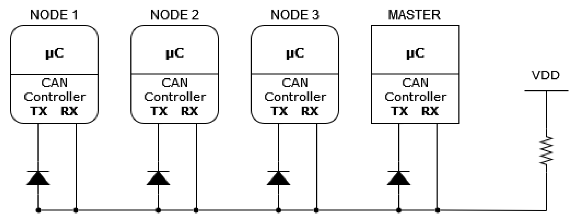
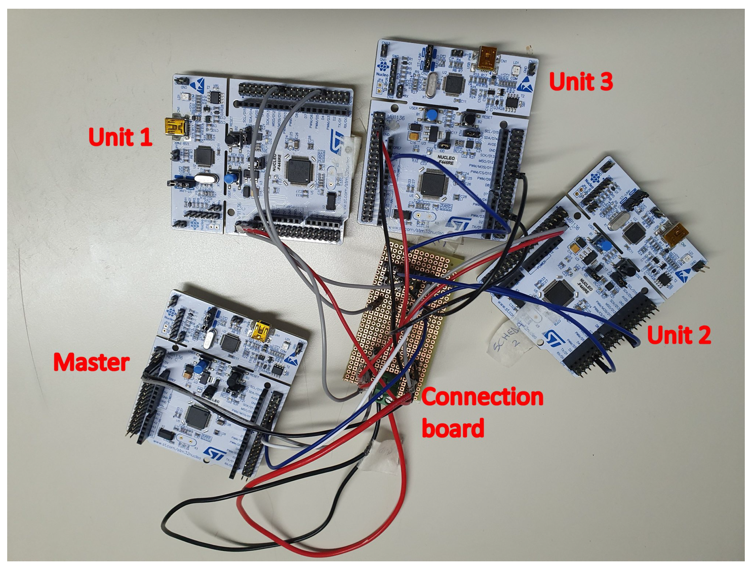
2. Materials and Methods

Unless additional impedance elements are used to connect the outputs of power converters in parallel, limiting the recirculating currents has to be achieved using only the natural resistance and inductance of the connections among the units. In particular, given the intrinsically transient operation of high frequency switch mode converters, the arising of recirculating currents is delayed only by the stray inductance, that for typical cable lengths of tens of centimeters can be estimated as a few hundred nanohenries [21]. Such a small inductance requires the PWM outputs of parallel converters to be synchronized at the picosecond level, which justifies the proposed two-stage approach. This is true even considering the damping effect of the stray resistance, mostly related to the on-state resistance of the power switches rather than to the one of copper traces and wires [22].
The initial synchronization has to minimize the delay error between parallel units in order to reduce the circulating currents after startup. Experimental validation has been done on identical MCU evaluation boards connected through CAN bus interface to a higher level control unit (master) managing the system. The hardware used for the units and the master is the ST NUCLEO-F446RE evaluation board with the STM32F446RE MCU. This hardware provides CAN peripherals and advanced controls timers embedded in the MCU for PWM generation with complementary outputs and dead time insertion, suitable for inverter control. The MCU is an ARM® Cortex® M4 with embedded FLASH, SRAM and 32 bit FPU that, combined with 12-bit ADCs, can also support the secondary fine synchronization control stage; this is not discussed in this paper.
Figure 1 is a diagram of the test bench used for this work. As can be seen, CAN tranceivers are not used to adapt the voltage levels to those required by the CAN protocol because the tests are done with short connections to avoid any disturbance problems. The diodes are used for monitoring purposes during tests, since they allow us to discriminate which unit is transmitting a dominant bit on the bus. The physical experimental setup is shown in Figure 2.

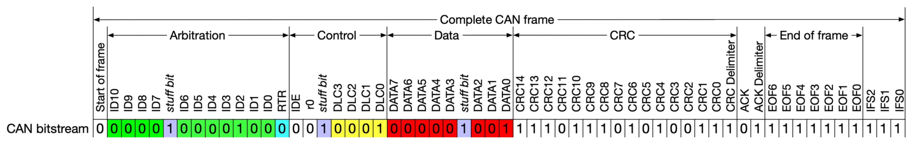
2.1. CAN Peripheral Synchronization Method

The CAN bus protocol is widely used in automotive and industrial embedded applications because of its robustness towards electromagnetic interference (EMI), which makes it suitable for communications between voltage source converters. To understand how the strategy works, it is necessary to introduce the bit timing properties of CAN bus. As will be clear in the following, the bit rate of the CAN network affects the precision achievable through the proposed technique (the faster the better). A bit rate is usually chosen based on the interference level and maximum distance between nodes in the final application; in this work a comparatively slow speed communication (100 kbit/s) was chosen in order to assess the level of synchronization obtainable in slow communications scenarios. The peripherals connected to CAN bus use a particular synchronization method based on division of total bit time into fixed-length time units called time quanta. There are different segments in a bit time:
  • Synchronization segment: where an edge is expected to be.
  • Propagation segment: used to compensate line and drivers delay.
  • Phase segments 1 and 2: dynamic length segments used to perform synchronization.
Two processes are involved in synchronization: hard synchronization, which is done at the beginning of each message to align segment slots between all nodes and soft synchronization, and soft synchronization, which is done by each node, lengthening phase segment 1 or shortening phase segment 2 by an integer number of time quanta, in order to compensate lagging or leading edges.

2.2. Oscillators Tolerance

The boards used in tests mount an external 8 MHz crystal oscillator. Due to temperature, voltage, capacitor tolerance and long term state of wear, frequency drift between units is unavoidable. As a consequence, CAN controllers on different units show frequency drift as well, which brings different peripherals to sample the same bit at different times. One of the goals of this work is to prove that synchronizing units on a common bus event leads to a residual PWM starting delay that depends on system frequency drift and not on the CAN bus resynchronization process.
Oscillator tolerance is obtained by an indirect measurement of alignment time of PWM signals, nominally identical, generated by the nodes. Due to different periods (clock frequency drift), a progressive time shift is found between corresponding rising/falling edges, so, by measuring the interval between two consecutive alignments of the rising edge ( T S Y ), the frequency drift can be derived as follows. Considering two PWM signals generated by different oscillators with periods T 1 and T 2 , respectively, during an interval T S Y , a number of N 1 periods are counted for the first PWM generator and N 2 are counted for the second, with T S Y = N 1 T 1 = N 2 T 2 . Considering T 1 > T 2 leads to:
N 1 = N , N 2 = N 1 + 1 = N + 1
T 1 = T S Y N , T 2 = T S Y N + 1
Normalizing periods difference to nominal switching period T s w and using Equations (1) and (2):
Δ T n o r m = T 1 T 2 T s w = 1 N ( N + 1 ) T S Y T s w
Considering that T s w is approximately equal to the average of the periods of the two units ( T s w T 1 + T 2 2 ) and using (2):
Δ T n o r m 1 N ( N + 1 ) T S Y T 1 + T 2 2 = 2 2 N + 1
Since T S Y T s w :
N T S Y T s w
A PWM frequency of 10 kHz nominal was generated for the experimental measurement of realignment times. As an example, the realignment of converter 2 and converter 1 took an average of 20.61 s over 303 measurements (Table 1). This value of T S Y translates into a number of cycles N before realignment of about 206,100.

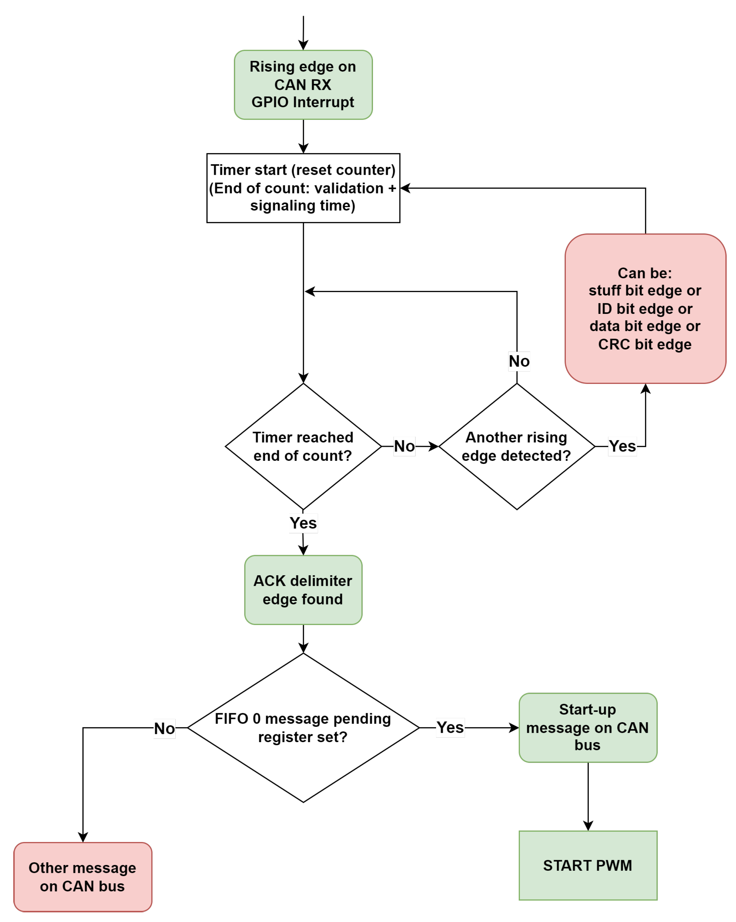
2.3. CAN Peripheral Interrupt Synchronization

Two different converter synchronization techniques have been tried in this work. The first one relies on the response of the CAN communication peripheral to a specific converter start-up message issued by the master controller. Robustness and versatility of the CAN protocol coexist with a big limitation in applications with very strong real time constraints, like in parallelization of VSCs without filters, where precise initial synchronization is needed to ensure the system integrity. CAN ensures a synchronization process at level 1 of the ISO/OSI stack that is used to compensate for the natural drift of local oscillators. This resynchronization process can lengthen or shorten the bit time at fixed steps determined by peripheral clock frequency, that in most cases is much lower than the system clock frequency. The CAN controller used in these tests, for example, can work at 45 MHz maximum frequency so that, with the limitation of phase segments length, bit time can be shortened or lengthened by 22 n s . In many cases due to noisy environment, the peripheral cannot work at this maximum speed so, the sampling process of bits in the CAN packet, improves uncertainty at lower speed like as demonstrated in this test.
The on board CAN peripheral (bxCAN) offers an hardware HLP (Higher Layer Protocol) at the data link level of the ISO/OSI stack managing:
  • Transmission and reception of incoming messages;
  • Construction of bit time (Time Quanta, Sync and Phase segments);
  • Interrupt management registers;
  • Diagnostic information.
The reception can be done using an input filter to store particular message IDs (in this case the converter start-up message) in particular FIFO stacks of the CAN peripheral. The presence of a message in a FIFO can cause a message pending (MP) interrupt, signaling the MCU that an incoming message should be read and causing a jump to the appropriate interrupt service routine (ISR). The ISR, in turn, starts the PWM, configured to generate a 100 μ s period.
The master unit periodically sends a starting message so that repeated tests of residual delay on first rising PWM edges can be done.
Due to the bit stuffing property of the CAN protocol, a valid message cannot have more than five consecutive bits with the same logical value except for the end of frame (EOF) field, which is composed by seven recessive bits. This makes it easy to recognize the acknowledge (ACK) that can be used as a common synchronization point for the PWM generation. The time period between the last rising edge of the CAN packet (ACK) (Figure 3) and the first rising edge of the PWM can be divided into four different subperiods:
  • Validation;
  • Peripheral FIFO register signaling;
  • Interrupt management (ends with first instruction of ISR);
  • PWM starting sequence.
It is clear that the first subperiod is bit-rate-dependent, because the message is valid for the receivers, if there is no error until the last but one bit of the EOF [23]. The last two subperiods are inserted by the MCU that is peripheral-frequency-independent, so it is logical to consider the sum of these periods fixed and deterministic because all units are subjected to the same calculation load.

2.4. GPIO Interrupt Synchronization

Leaving the synchronization to the CAN peripheral interrupt brings uncertainties especially when the time quantum (TQ) is large, as shown in the results section. Therefore, a second strategy was tested, in which the synchronization is performed using the general-purpose input–output (GPIO) peripheral of the MCU. With this strategy, one line of the CAN bus is also routed to a GPIO pin set up as an input, while the CAN peripheral is used to recognize the start-up message. The GPIO pin raises an interrupt whenever a rising edge is detected in a CAN packet. This happens regardless of the message that has been sent, so a particular algorithm (Figure 4) is used to discriminate the start-up event.
Each time a new GPIO interrupt event occurs, a timer starts counting up from zero. The timer is set to raise an interrupt event after an interval that is the sum of the validation and peripheral signaling subperiods previously defined. This delay ensures the CAN peripheral has enough time to store an incoming message in the FIFO and set the corresponding register. Crucially, the delay is also longer than the longest possible stream of bits of the same value, so the timeout will only occur after the last edge of a CAN packet, that is the ACK delimiter edge. At this time, the algorithm knows that a CAN message has been fully transmitted and correctly received, but it still needs to check if the message was indeed a start-up message from the master node. The timer ISR, therefore, instructs the MCU to poll the CAN peripheral FIFO: if a start-up message is found, the PWM is finally started. This solution ensures that all the units are synchronized on a common event (ACK) caused by the slowest node. The timer count is clock drift dependent, but not CAN peripheral synchronization dependent.

3. Results

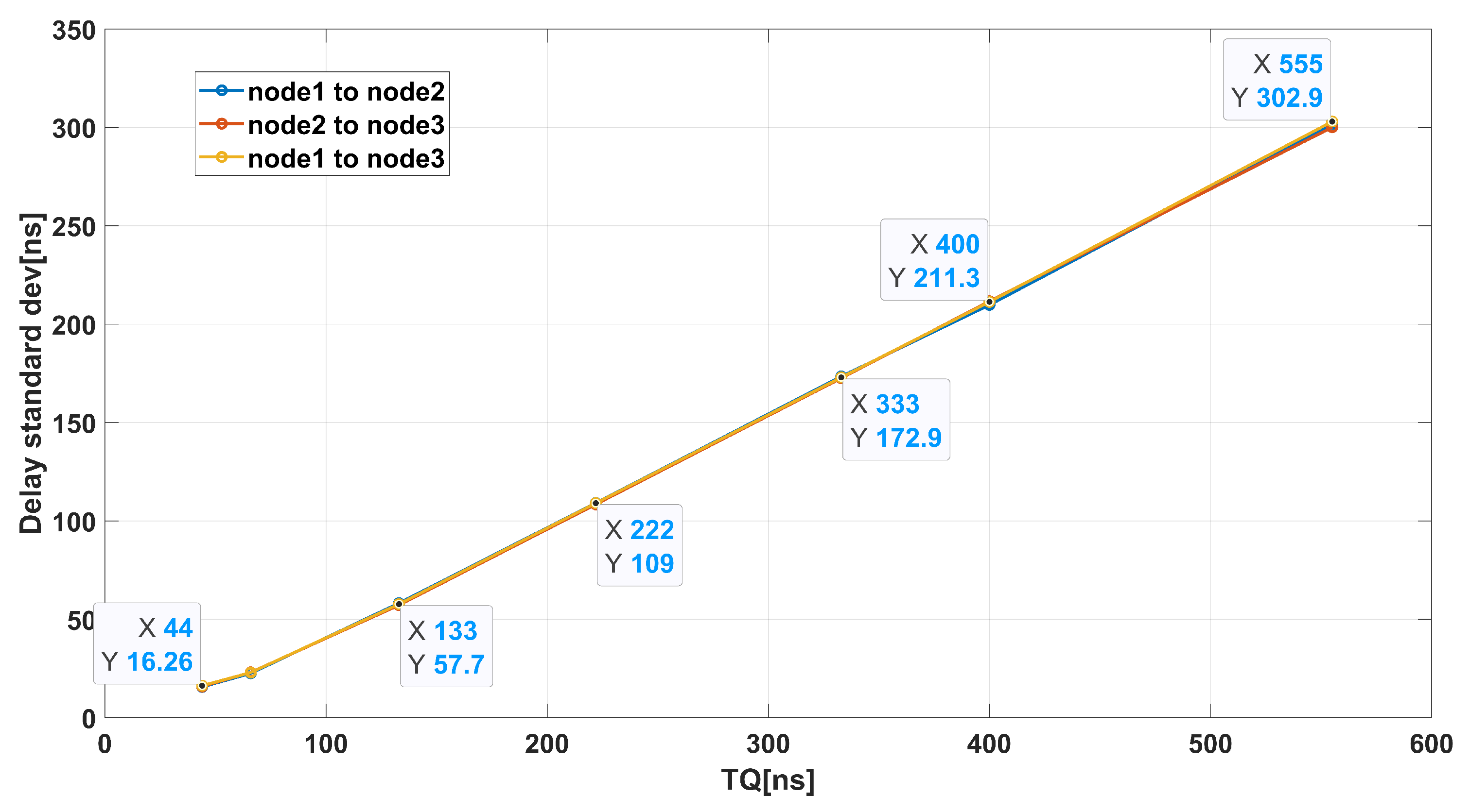
3.1. Frequency Drift

Measurements of the realignment time ( T S Y ) between each pair of nodes are reported in Table 1, where 2 1 indicates the realignment time between the PWM signals of converter 2 and converter 1, and similarly for the other pairs of units. Data was captured using the statistical functions of a digital storage oscilloscope (Figure 5).
Combining the results of Table 1 and Table 2 confirms the intuitive idea that increasing realignment time results in a smaller oscillator mismatch, i.e., frequencies are better matched. The values in Table 2 confirm that, even if all the microcontrollers are clocked by quartz oscillators of the same nominal value, the actual clock frequencies are randomly dispersed. This frequency mismatch, although small, if left uncontrolled, can quickly lead to arbitrarily large phase differences, which justifies the need for a closed loop control (not described in this paper) to strictly maintain the required phase match after the initial alignment.
Considering Equations (4) and (5), it is possible to estimate the relative oscillator tolerance between units. These tolerances are reported in Table 2.

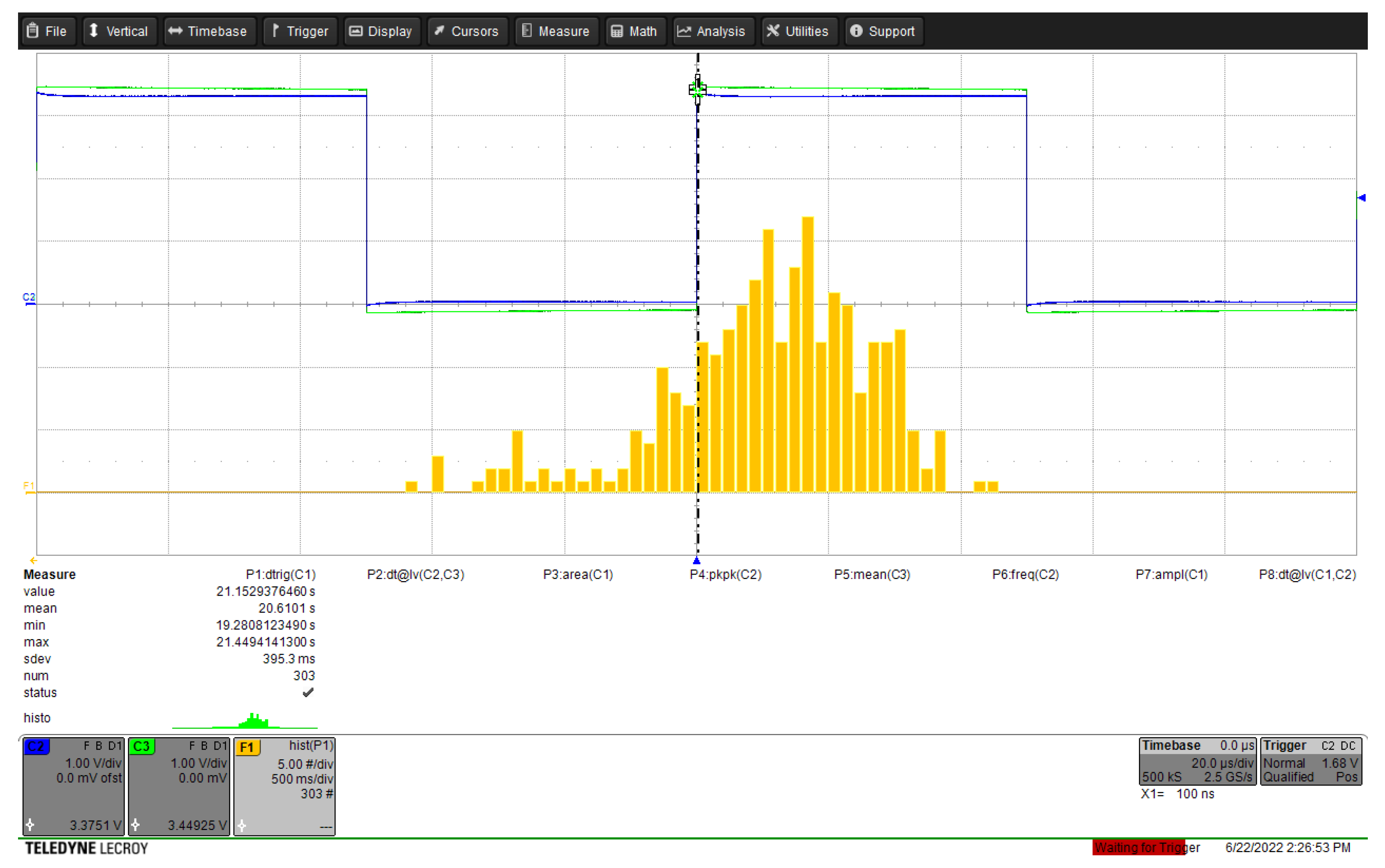
3.2. CAN Peripheral Interrupt Synchronization

Tests on residual PWM delays inserted by preliminary synchronization using CAN peripheral interrupt are shown in Figure 6. Tests were performed between pairs of units, whereas one unit was sending the start-up message and both were trying to synchronize their PWM generators based upon the arrival of the message in the CAN buffer. It can be seen that the standard deviations of the three relative delays change monotonically with an increase of TQ.
The monotonical increasing trend confirms that, with larger TQ, the CAN peripheral can make larger bit-time jumps to synchronize units, resulting in a less precise overall synchronization.
Different bit rates can be obtained using the same TQ by modifying the phase segments length during CAN initialization. The results in Table 3 show that increasing the bit rate with the same TQ does not result in a better synchronization, so it is clear that synchronization precision depends more on TQ than on the CAN bit rate.

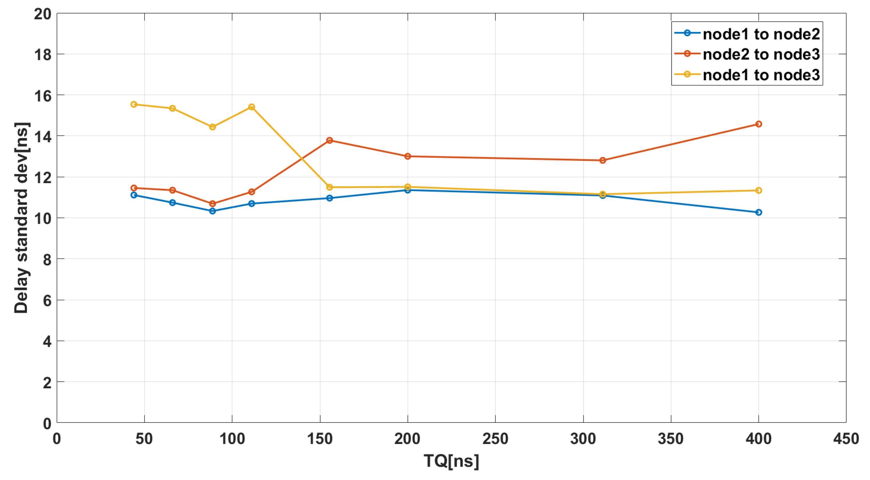
3.3. GPIO Interrupt Synchronization

This test was performed on pairs of units, similarly to the CAN peripheral synchronization test. In this case, the CAN signal was routed in parallel to a GPIO input and the algorithm of Figure 4 was used to synchronize the start of the PWM generation. The results are reported in Figure 7.
The results show that this synchronization method is TQ independent because the parallel units have a common synchronization point (the last rising edge of the message) and then the uncertainty is given only by the timer peripheral, which is strongly related with oscillator tolerance. The independence from TQ yields a synchronization precision over an order of magnitude better for this second method compared with the first one with large TQ.

4. Conclusions

The goal of a less than 1 % synchronization error between parallel converters PWM signals can be achieved using both methods presented in this paper. The difference is that the CAN peripheral interrupt method is strongly related to the CAN peripheral behavior; using, for example, a 550 ns TQ results in a synchronization uncertainty that is more than the required 1 % . It is clear that the results in Figure 6 represent the standard deviation of the delay, but some bad cases have been recorded during tests, where the delay was higher than 1   μ s so that, with a 100   μ s PWM period, the specification was not met.
The GPIO interrupt method is intrinsically CAN peripheral independent and tests have shown a less than 0.1 % synchronization error, one order of magnitude better than the requirements, even in the worst case.
This work paves the way for the second phase (fine synchronization) that is required to parallelize converters without any reactive filters.

Author Contributions

Conceptualization, A.S. and C.C.; methodology, A.S.; software, G.L.R.; validation, A.S., C.C. and M.B.; formal analysis, A.S. and G.L.R.; investigation, A.S., C.C. and G.L.R.; writing—original draft preparation, G.L.R.; writing—review and editing, C.C., A.S. and M.B.; visualization, G.L.R. and M.B.; supervision, A.S. and C.C.; project administration, A.S.; funding acquisition, A.S. All authors have read and agreed to the published version of the manuscript.

Funding

This research has financially been supported by the Programme “FIL-Quota Incentivante” of University of Parma and co-sponsored by Fondazione Cariparma, under the project REBASED (REduced-BAllast distributed power converters for Safety, Efficiency and power Density).

Data Availability Statement

Not applicable.

Conflicts of Interest

The authors declare no conflict of interest.

References

  1. Zhang, J.; Li, Y.; Wang, H.; Cai, X.; Igarashi, S.; Wang, Z. Thermal smooth control based on orthogonal circulating current for multi-MW parallel wind power converter. In Proceedings of the 2014 International Power Electronics and Application Conference and Exposition, Shanghai, China, 5–8 November 2014; IEEE: Shanghai, China, 2014; pp. 146–151. [Google Scholar] [CrossRef]
  2. Li, W.; Zhang, X.; Zhuang, Y.; Zhang, G.; Wang, G.; Xu, D. A Five-Level Space Vector Modulation Scheme for Parallel Operated Three-Level Inverters With Reduced Line Current Distortion. IEEE Trans. Power Electron. 2020, 35, 11235–11249. [Google Scholar] [CrossRef]
  3. Tan, L.; Zhu, N.; Wu, B. An Integrated Inductor for Eliminating Circulating Current of Parallel Three-Level DC–DC Converter-Based EV Fast Charger. IEEE Trans. Ind. Electron. 2016, 63, 1362–1371. [Google Scholar] [CrossRef]
  4. Rodriguez-Amenedo, J.L.; Arnaltes-Gomez, S.; Aragues-Penalba, M.; Gomis-Bellmunt, O. Control of the Parallel Operation of VSC-HVDC Links Connected to an Offshore Wind Farm. IEEE Trans. Power Deliv. 2019, 34, 32–41. [Google Scholar] [CrossRef] [Green Version]
  5. Kim, S.A.; Han, S.W.; Byun, S.I.; Cho, Y.H. Improved parallel operation mode control of parallel connected 12-pulse thyristor dual converter for urban railway power substations. In Proceedings of the 2016 IEEE 17th Workshop on Control and Modeling for Power Electronics (COMPEL), Trondheim, Norway, 27–30 June 2016; IEEE: Trondheim, Norway, 2016; pp. 1–6. [Google Scholar] [CrossRef]
  6. Arnaudov, D.D.; Vuchev, S.A. Investigation of Resonant Converters Parallel Operation to a Common Load. In Proceedings of the 2018 IEEE XXVII International Scientific Conference Electronics-ET, Sozopol, Bulgaria, 13–15 September 2018; IEEE: Sozopol, Bulgaria, 2018; pp. 1–4. [Google Scholar] [CrossRef]
  7. Chen, T.P. Zero-Sequence Circulating Current Reduction Method for Parallel HEPWM Inverters Between AC Bus and DC Bus. IEEE Trans. Ind. Electron. 2012, 59, 290–300. [Google Scholar] [CrossRef]
  8. Xueguang, Z.; Wenjie, Z.; Jiaming, C.; Dianguo, X. Deadbeat Control Strategy of Circulating Currents in Parallel Connection System of Three-Phase PWM Converter. IEEE Trans. Energy Convers. 2014, 29, 406–417. [Google Scholar] [CrossRef]
  9. Yu, H.; Tao, Y.; Li, G.J.; Yin, S.; Zhuang, J.; Sun, C. Control Strategy for Parallel Operation of Converters Based on Adaptive Virtual Inductance. In Proceedings of the 2021 International Conference on Wireless Communications and Smart Grid (ICWCSG), Hangzhou, China, 13–15 August 2021; IEEE: Hangzhou, China, 2021; pp. 444–448. [Google Scholar] [CrossRef]
  10. Li, D.; Huang, X.; Nie, C.; Niu, J.; Chen, R.; Lin, M.; Ji, S.; Wang, F.; Tolbert, L.M.; Giewont, W. Paralleling Operation of 10 kV SiC MOSFET-Based Modular Multi-Level Converters (MMCs) for Scalable Asynchronous Microgrid Power Conditioning System. In Proceedings of the 2021 IEEE Applied Power Electronics Conference and Exposition (APEC), Phoenix, AZ, USA, 14–17 June 2021; IEEE: Phoenix, AZ, USA, 2021; pp. 1444–1450. [Google Scholar] [CrossRef]
  11. Choo, K.L. Parallel connection of DC/AC switched mode power converter in utility distribution system. In Proceedings of the 2008 IEEE 2nd International Power and Energy Conference, Johor Bahru, Malaysia, 1–3 December 2008; IEEE: Johor Bahru, Malaysia, 2008; pp. 1369–1372. [Google Scholar] [CrossRef]
  12. Gan, J.; Yin, Q.; Chen, T.; Zhao, L.; Deng, C.; Liu, Z. Reasearch on the circulating current suppression for parallel T-type three-level PCS based on on-line synchronization and average current. In Proceedings of the 2019 IEEE 3rd Advanced Information Management, Communicates, Electronic and Automation Control Conference (IMCEC), Chongqing, China, 11–13 October 2019; IEEE: Chongqing, China, 2019; pp. 773–776. [Google Scholar] [CrossRef]
  13. Gohil, G.; Bede, L.; Teodorescu, R.; Kerekes, T.; Blaabjerg, F. Evaluation of circulating current suppression methods for parallel interleaved inverters. In Proceedings of the 2016 IEEE Energy Conversion Congress and Exposition (ECCE), Milwaukee, WI, USA, 18–22 September 2016; IEEE: Milwaukee, WI, USA, 2016; pp. 1–8. [Google Scholar] [CrossRef]
  14. Asiminoaei, L.; Aeloiza, E.; Kim, J.; Enjeti, P.; Blaabjerg, F.; Moran, L.; Sul, S. Parallel Interleaved Inverters for Reactive Power and Harmonic Compensation. In Proceedings of the 37th IEEE Power Electronics Specialists Conference, Jeju, Republic of Korea, 18–22 June 2006; IEEE: Jeju, Republic of Korea, 2006; pp. 1–7. [Google Scholar] [CrossRef]
  15. Rannestad, B.; Munk-Nielsen, S.; Gadgaard, K. Discontinuous interleaving of parallel inverters for efficiency improvement. In Proceedings of the 2017 19th European Conference on Power Electronics and Applications (EPE’17 ECCE Europe), Warsaw, Poland, 11–14 September 2017; IEEE: Warsaw, Poland, 2017; pp. P.1–P.10. [Google Scholar] [CrossRef]
  16. Gohil, G.; Bede, L.; Teodorescu, R.; Kerekes, T.; Blaabjerg, F. An Integrated Inductor for Parallel Interleaved Three-Phase Voltage Source Converters. IEEE Trans. Power Electron. 2016, 31, 3400–3414. [Google Scholar] [CrossRef] [Green Version]
  17. Trintis, I.; Gohil, G.; Wurzer, M.; Franzen, M.; Pallesgaard, S.L.; Munk-Nielsen, S.; Carne Kjaer, P. Line reactor for parallel-interleaved high power inverters. In Proceedings of the 2017 19th European Conference on Power Electronics and Applications (EPE’17 ECCE Europe), Warsaw, Poland, 11–14 September 2017; IEEE: Warsaw, Poland, 2017; pp. P.1–P.10. [Google Scholar] [CrossRef]
  18. Gohil, G.; Bede, L.; Teodorescu, R.; Kerekes, T.; Blaabjerg, F. Magnetic Integration for Parallel Interleaved VSCs Connected in a Whiffletree Configuration. IEEE Trans. Power Electron. 2016, 31, 7797–7808. [Google Scholar] [CrossRef] [Green Version]
  19. Zhang, D.; Wang, F.; Burgos, R.; Boroyevich, D. Total Flux Minimization Control for Integrated Inter-Phase Inductors in Paralleled, Interleaved Three-Phase Two-Level Voltage-Source Converters With Discontinuous Space-Vector Modulation. IEEE Trans. Power Electron. 2012, 27, 1679–1688. [Google Scholar] [CrossRef]
  20. Soldati, A.; Undre, V.; Concari, C.; Alsayid, B.A.; Dradi, M.H. Parallel Operation of Voltage Source Converters without Filter Inductors: Control of the Circulating Current. In Proceedings of the 2020 2nd IEEE International Conference on Industrial Electronics for Sustainable Energy Systems (IESES), Cagliari, Italy, 1–3 September 2020; IEEE: Cagliari, Italy, 2020; pp. 125–130. [Google Scholar] [CrossRef]
  21. Rumble, J. CRC Handbook of Chemistry and Physics: A Ready-Reference Book of Chemical and Physical Data, 102nd ed.; CRC Press: Boca Raton, FL, USA, 2021. [Google Scholar]
  22. Reatti, A.; Corti, F.; Tesi, A.; Torlai, A.; Kazimierczuk, M.K. Effect of Parasitic Components on Dynamic Performance of Power Stages of DC-DC PWM Buck and Boost Converters in CCM. In Proceedings of the 2019 IEEE International Symposium on Circuits and Systems (ISCAS), Sapporo, Japan, 26–29 May 2019; IEEE: Sapporo, Japan, 2019; pp. 1–5. [Google Scholar] [CrossRef]
  23. ISO 11898; CAN Specification Version 2.0. Bosch: Gailingen, Germany, 1991; pp. 1–72.
Figure 1. Principle diagram of the test bench. The master triggers three slave nodes, which synchronize themselves following the technique proposed in this paper. The CAN line is configured for wired and operation.
Applsci 13 00230 g001
Figure 2. Photo of the test setup.
Applsci 13 00230 g002
Figure 3. Example of CAN bus frame. Green bits make up the message ID field, yellow bits are DLC (data length code), red are data bits, violet are stuff bits. Image courtesy of Ken Tindell, Canis Automotive Labs Ltd, through Wikipedia.
Applsci 13 00230 g003
Figure 4. Start message detection algorithm.
Applsci 13 00230 g004
Figure 5. Experimental determination of realignment time statistics between the PWM signals of converter 2 and converter 1.
Applsci 13 00230 g005
Figure 6. CAN peripheral synchronization: standard deviations of delays as a function of time quantum.
Applsci 13 00230 g006
Figure 7. GPIO peripheral synchronization: standard deviations of delays as a function of the time quantum.
Applsci 13 00230 g007
Table 1. Alignment test results.
Units under TestN (Number of Tests)Average [s]Std. Dev. [ms]Minimum [s]Maximum [s]
2 1 303 20.61 395.3 19.28 21.15
3 1 338 7.79 161.5 7.49 8.24
3 2 314 5.59 79.91 5.39 5.78
Table 2. Oscillator mismatch between each pair of units.
Units under TestOscillator Mismatch [ppm]
2 1 4.85
3 1 12.83
3 2 17.89
Table 3. Standard deviations of three delays with different bit rates.
Delay Sigma 200 kbit s @ TQ = 200 ns 1 Mbit s @ TQ = 200 ns
2 1 [ σ 21 ] 96.23   n s 110.1   n s
3 1 [ σ 31 ] 115.6   n s 135.2   n s
3 2 [ σ 32 ] 95.40   n s 112.1   n s
Disclaimer/Publisher’s Note: The statements, opinions and data contained in all publications are solely those of the individual author(s) and contributor(s) and not of MDPI and/or the editor(s). MDPI and/or the editor(s) disclaim responsibility for any injury to people or property resulting from any ideas, methods, instructions or products referred to in the content.

