Article

On the Absorption and Photoluminescence Properties of Pure ZnSe and Co-Doped ZnSe:Eu3+/Yb3+ Crystals

by
Behnaz Abbasgholi-NA
1,
Osamah A. Aldaghri
2,
Khalid Hassan Ibnouf
2,
Nawal Madkhali
2,* and
Humberto Cabrera
1,*
1
Optics Lab, STI Unit, The Abdus Salam International Centre for Theoretical Physics, Strada Costiera 11, 34151 Trieste, Italy
2
Physics Department, College of Sciences, Imam Mohammad Ibn Saud Islamic University (IMSIU), Riyadh 13318, Saudi Arabia
*
Authors to whom correspondence should be addressed.
Appl. Sci. 2022, 12(9), 4248; https://doi.org/10.3390/app12094248
Submission received: 27 February 2022 / Revised: 14 April 2022 / Accepted: 20 April 2022 / Published: 22 April 2022
(This article belongs to the Special Issue Investigation and Design of Novel Materials for Photonic Applications)

Abstract

:
Co-doped Zinc selenide (ZnSe) is a promising material because of a high photoluminescence efficiency and wide spectral range emission in the visible region. In this work, ZnSe and Eu3+/Yb3+ co-doped ZnSe crystals were grown by the chemical vapour transport method. Photoluminescence and optical measurements revealed the effect of trivalent rare earth Eu3+/Yb3+ ions on the emission of new lines with enhancement intensity. In the photoluminescence spectrum, some sharp and intense lines were observed that allow for the possibility of covering a broad emission range. Moreover, the optical measurement showed a lower bandgap compared to that of pure ZnSe bulk crystal. This material is suitable for developing optoelectronic devices, which can emit light in the visible and near infrared range with an improved emission efficiency and wide tunability.

1. Introduction

New materials, hetero-structures, hetero-junctions, and doped single crystal have been the subject of numerous studies to produce optoelectronics devices emitting from blue to near-IR region [1]. Recent applications such as high-density optical memories, display devices, and biological applications require solid-state semiconductor laser and light emitting diodes (LED) emitting in the blue and green wavelengths. Others, for example, the LED of high efficiency for illumination, require high as well as low wavelengths to illuminate inner spaces. The possible semiconductors that emit light in these wavelengths are the ones of the II–VI semiconductor family. These materials have direct gap edge of energy capable of emitting photons with a wavelength less than 500 nm.
Investigations for laser devices with materials such as GaN and ZnSe have had a tremendous progress in the last thirty years. In 1991, a ZnCdSe/ZnSe quantum well laser diode successfully demonstrated a pulsed operation at room temperature [2]. The first solid-state semiconductor blue-green laser and light emitting diode (LED) were built in 1991–1992 using wide band gap II–VI semiconductors with a ZnSe-based single quantum well structure [3,4]. A GaN/AlGaN double-heterostructure has shown optically a pumped lasing in the UV region at room temperature [5]. High efficiency InGaN/GaN double-heterostructure LEDs have also been obtained [6]. Other materials and technologies to produce compact diode-pumped Nd: LuVO4 solid state lasers have been studied [7] as well as the high-efficiency nitride semiconductor blue lasers and light emitting diodes [8].
ZnSe is chemically stable metal chalcogenide, which possesses many advantages, making it an important optoelectronic material. It has useful electronic properties such as a wide and direct bandgap, low electrical resistivity, and n-type conductivity. Regarding optical properties, it has a broad transparency from visible to mid infrared wavelengths, high refractive index, low dispersion, and high photosensitivity. From the other side, the trivalent rare earth ions are particularly useful because they produce additional lines and enhance the intensity of the emission spectra because f-electron absorption transitions are much weaker than those of the d electrons. This allows for the use of much higher active ion concentrations without complications from extensive self-absorption or excitation depletion.
Recently several papers have reported on the luminescence of II–VI semiconductors doped with Tb3+, Sm2+, Eu3+/Eu2+, or Er [8,9] particularly on the luminescence of ZnSe:Eu3+ and ZnSe:Yb [10,11]. Moreover, the co-doping with two rare earths gives the possibility of optical pumping between the f electron quantum levels of one rare earth to the other. Additionally, Yb3+ has a relatively simple energy diagram presented by one excited state 2F5/2 and a ground 2F7/2 state lying ≈ 1.2 eV below, absence of the line widening, and absorption on the excited state [12]. Therefore, the energy level configuration of ZnSe: Eu3+/Yb3+ may generate transitions, which allow for a wider range of wavelengths in the photoluminescence spectrum. However, there have not been any reports on the photoluminescence properties of ZnSe co-doped with Eu3+ and Yb3+.
In this work, high quality single crystals were doped and co-doped with Eu3+/Yb3+ rare earths in order to obtain semiconductors with very high photoluminescence in the visible and near infrared region. The luminescence spectra of these materials give multiple intense and sharp emission lines. The material was characterized using photoluminescence and UV–Vis techniques in order to obtain their photoluminescence and absorption properties. This material exhibited new and more intense emission lines in the visible and near infrared spectral region, thus giving the possibility of developing high efficacy and tunable light emitting devices.

2. Materials and Methods

The samples were prepared by chemical vapour transport method using iodine as a transporting agent following the procedure reported elsewhere [13]. Pure ZnSe (purity was 99.99%) single crystal and the other samples doped with a single rare earth and co-doped with two rare earths Eu3+/Yb3+ were grown by this method. The binary compounds were synthesized first from the high purity elements by direct flame heating in quartz ampoules under vacuum. Then, the very high quality samples were produced after mixing in appropriate proportions with the concentration of the doping impurity. ZnSe crystals were doped with 1 mol % Eu3+ or co-doped with 1 mol % Eu3+ and 1 mol % Yb3+.
X-ray diffraction (XRD, Rigaku, Tokyo, Japan) with a monochromatic Cu kα target in 2 theta geometry was used to determine the crystal structure of the samples.
The crystallinity of the pure ZnSe single crystal was confirmed using grazing incidence X-ray diffraction with a grazing angle of 1° and 2θ in the range of 10°–80°, as shown in Figure 1. The results show a polycrystalline structure and a cubic zinc blende crystal structure with orientation mainly toward the (111) axis perpendicular to the surface.
The absorption spectra were taken for each sample as a function of temperature between 20 K to room temperature from 350 nm to 1100 nm. The experimental setup consisted of a closed cycle helium cooling system, with controlled temperature using a Cary 17D spectrophotometer.
Photoluminescence (PL) measurement is crucial for the registration of the emission spectra of new materials in order to calculate their efficiency and tunability [14,15]. In this direction, the spectra were recorded using a one-meter Spex monochromator equipped with a GaAs photomultiplier and the excitation source from an argon ion laser (Innova 300C series, Coherent USA) at 488 nm or 457.9 nm wavelengths operated at 10 mW power. The photoluminescence spectra were recorded using Labview data acquisition software as a function of temperature from 20 K to room temperature.
The basic algorithm procedure for the fitted experimental data is as follows. First, the data were normalized to minimize the computational processing time. Second, an error function based on a square mean error between the experimental data and the physical model was defined. Third, the parameters of the error function were optimized by genetic algorithms adapted to each particular situation. Finally, the parameters of the fitting function were obtained. The experimental data were fitted to theoretical models using the genetic algorithm routines briefly described above.

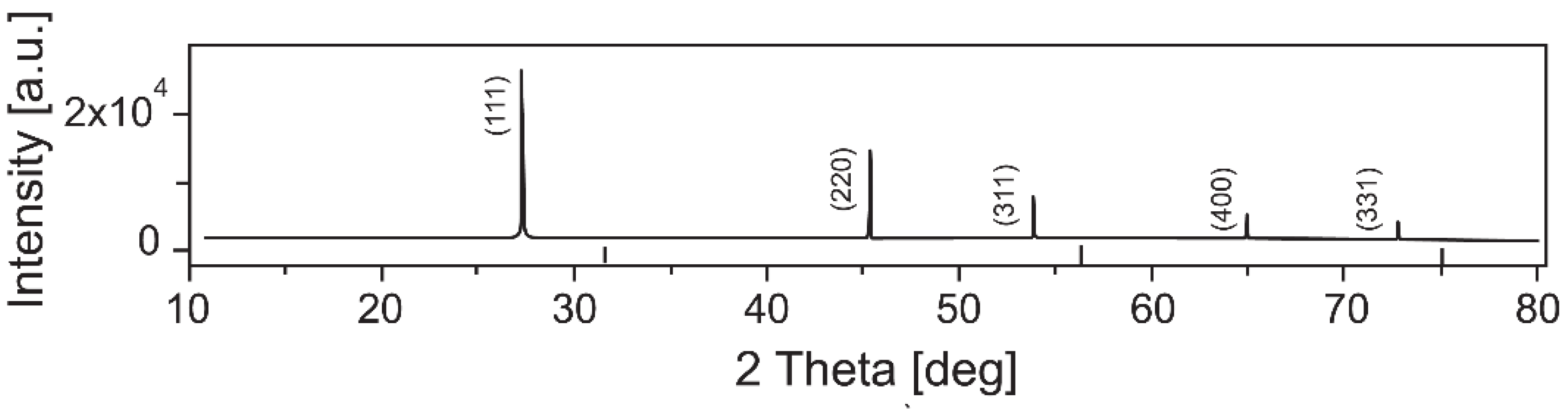
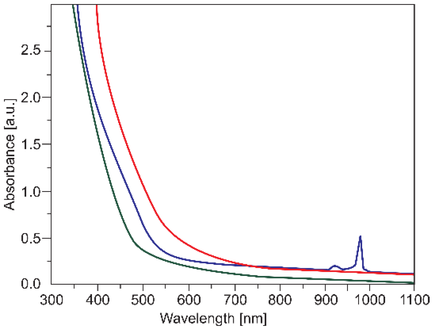
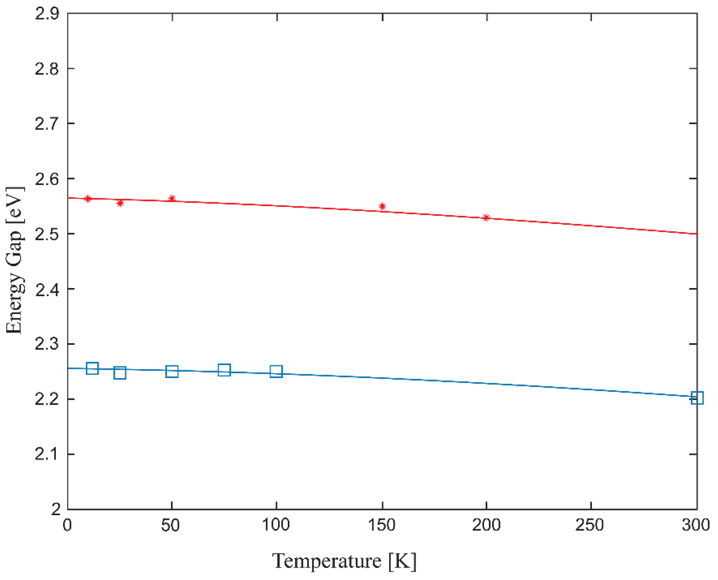
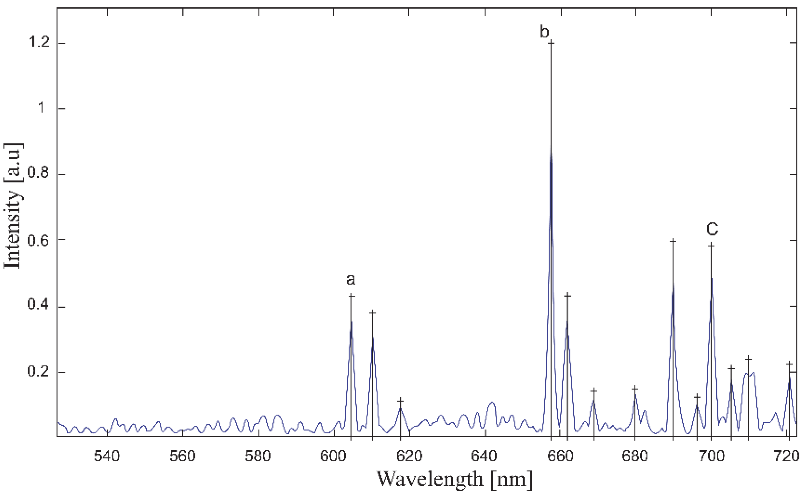
3. Results and Discussion

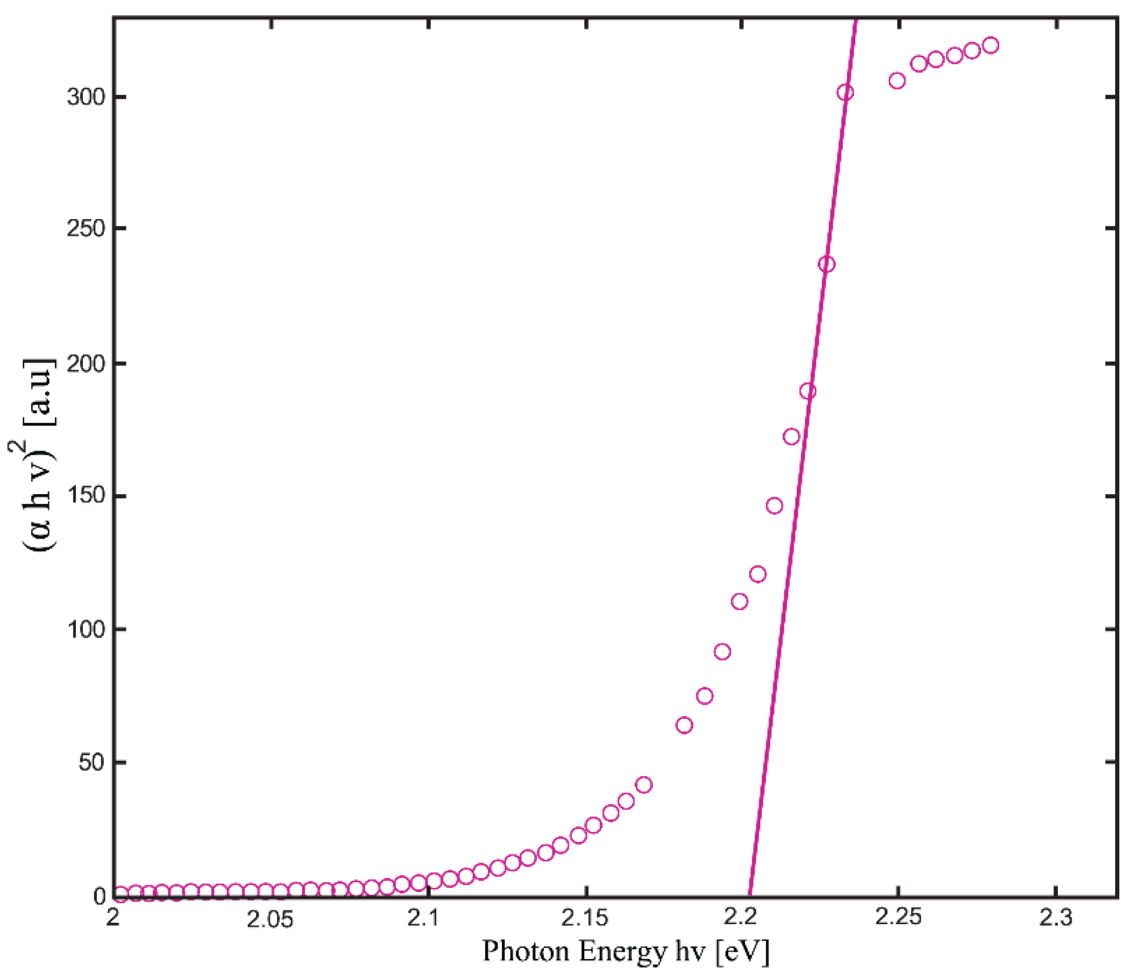
3.1. Absorption Measurement Energy Band Gap Determination

Theoretical analysis of the absorption coefficients α for the ZnSe pure materials and the doped ones show that they obey the following relations [16]:
α = A h ν h ν E g
where A is a parameter; Eg is the band gap of allowed transitions (eV); h is Planck’s constant (6.63 × 10⁻³⁴ Js); and υ is the frequency of the light (s−1). The values of band gaps were obtained from the absorption spectra at room temperature using a UV–Vis spectrophotometer (Figure 2). In all samples, the absorption edge was very sharp and was located at about 465 nm, 496 nm, and 563 nm for ZnSe, ZnSe:Eu3+Yb3+, and ZnSe:Eu3+, respectively. The obtained values were in quite good agreement with the literature reports [17,18]. In order to determine the values of the band gaps for the examined samples, we plotted the graph of [ α h υ ] 2 as a function of photon energy E = h υ . Extrapolation of the linear part of the graph gives the values of the band gap as the intercept with the abscissa axis, for which [ α h υ ] 2 = 0 . The determined values of band gaps for all examined samples are presented in Table 1 and the procedure is shown for the ZnSe:Eu3+ sample in Figure 3.
From the results presented in Table 1, it is clear that the bandgap energy of the doped and co-doped semiconductors decreased compared with the host matrix ZnSe (2.67 eV). It is well known that impurities generate additional donor and acceptor levels in the host material, which can produce drastic changes in the optical behaviour and reduce the band-gap energy.
The Varshni semi empirical relation [19] describes the energy band gap variation as a function of temperature for a doped semiconductor with different rare earths:
E ( T ) = E 0 ( 0 ) γ T 2 β + T
where E0(0) is the energy band gap value at T = 0 K; γ is a parameter related to the electron-phonon interaction; T is the absolute temperature; and β is a parameter related to the Debye temperature. A routine to fit the experimental data to the Varshni semi empirical relation was developed using a genetic algorithm. All Varshni semi empirical relation parameters were obtained using the developed routine, and are listed in Table 2. The energy band gap dependence with the temperature for ZnSe:Eu3+ and ZnSe:Eu3+/Yb3+ is shown in Figure 4.

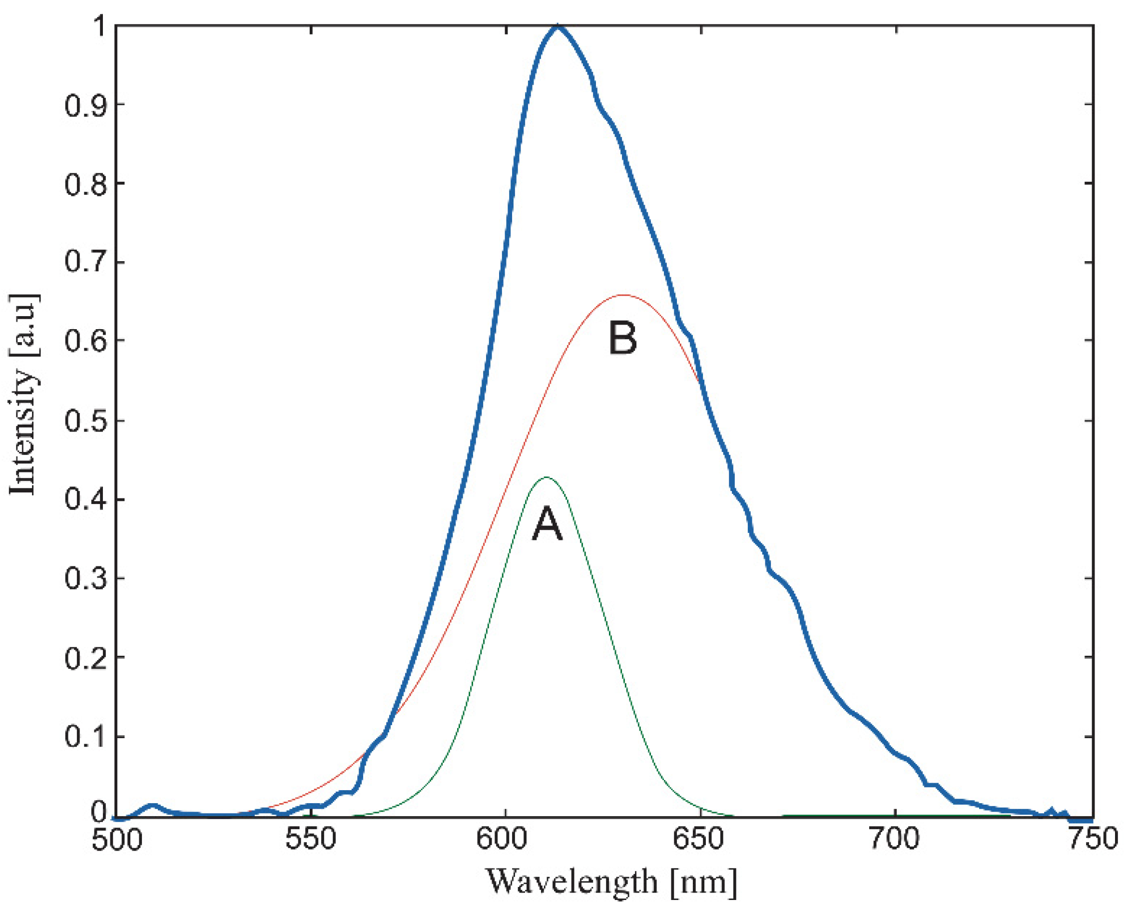
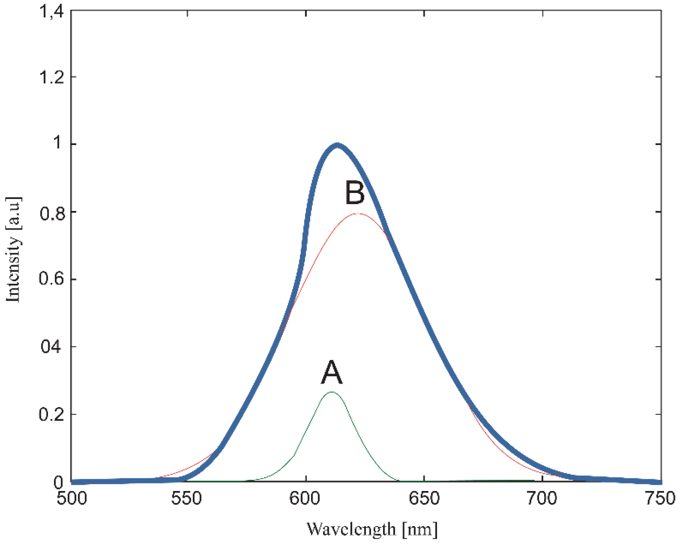
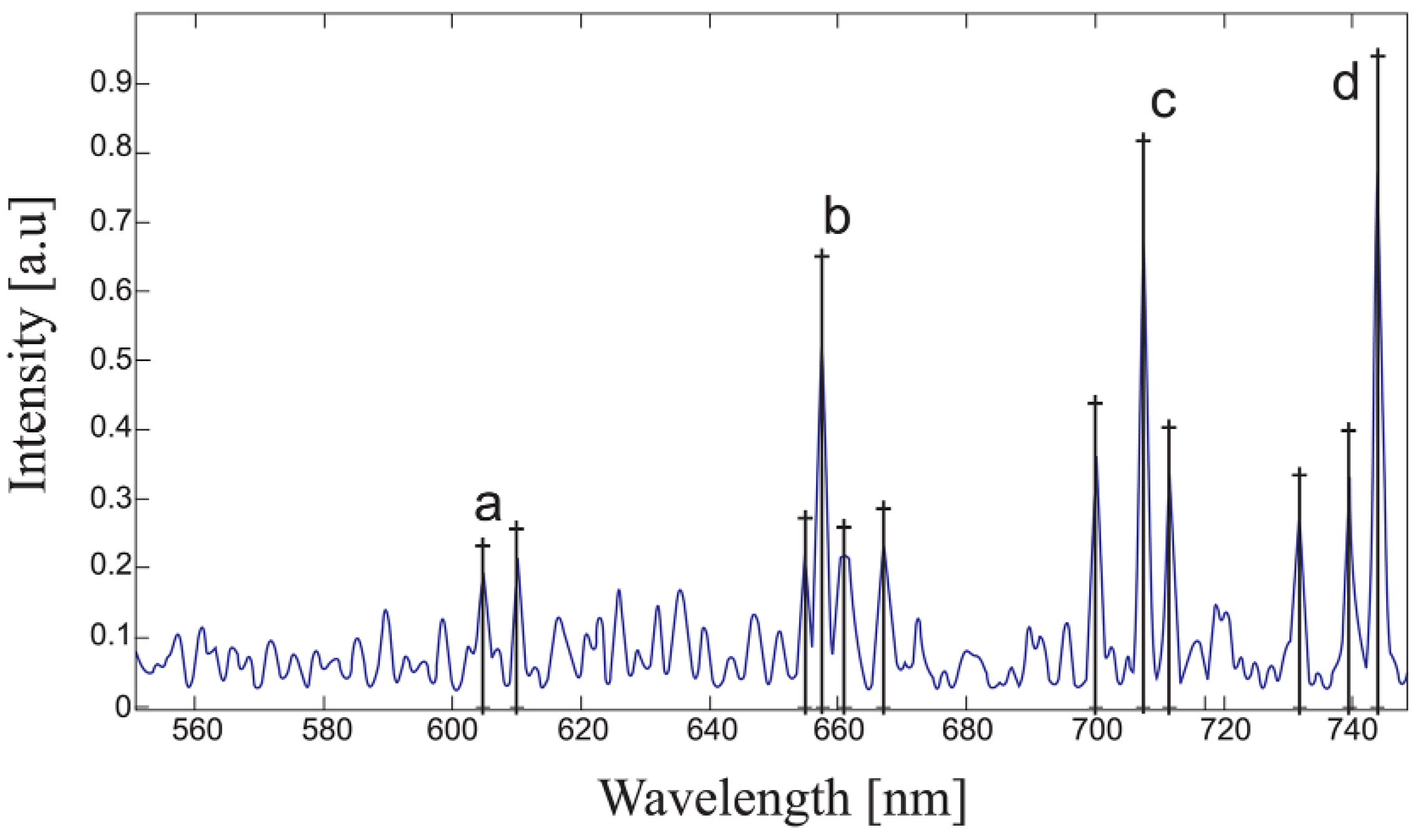
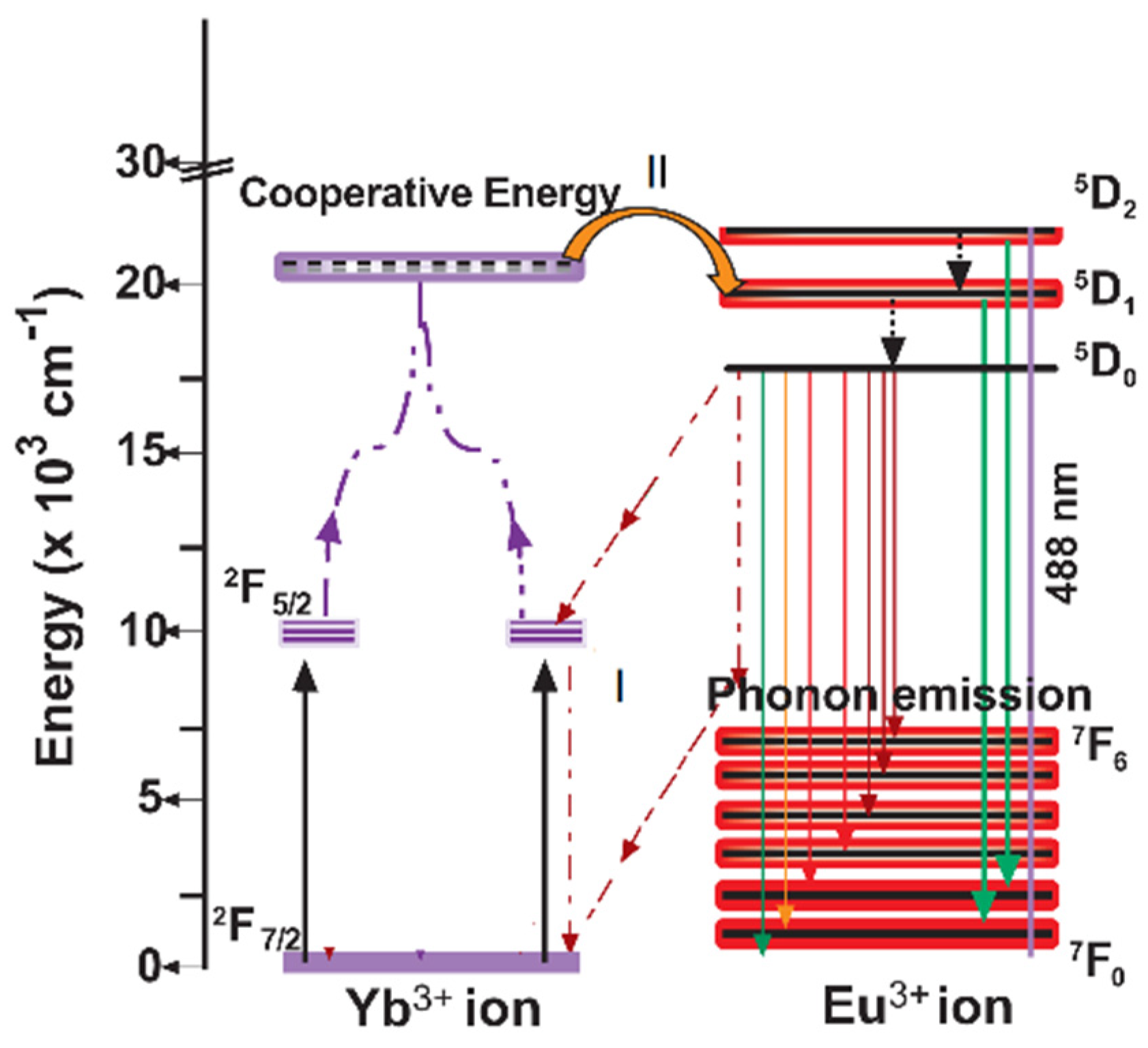
3.2. Photoluminescence Measurements

The photoluminescence emission spectrum for pure ZnSe is shown in Figure 5. Two bands A and B are seen in the figure. The B band was centred around 610 nm at low temperatures and showed a slight shift to the lower wavelengths decreasing with temperature, as shown in Table 3. The band A was centred at 637 nm at low temperature. The theoretical fitting of these curves as a function of temperature for the two bands gives the following equations, respectively:
λ A = 610.6 0.0247 T   ( nm )
λ B = 636 + 0.09 T 0.001 T 2   ( nm )
Figure 6 shows the photoluminescence emission when the ZnSe semiconductor was doped with a single rare earth Eu3+. The emission spectrum was the same as pure ZnSe (Figure 5), but band B was more intense. Moreover, the temperature at which the photoluminescence was detectable was higher (250 K), as shown in Table 4. This is an expected result because of the additional photon energy supplied by donor–acceptor levels created with the inclusion of Eu3+ ions in the crystal, which enables more efficient pumping.
Eu shows two valence states, trivalent (Eu3+) and divalent (Eu2+), in certain compounds. However, the co-existence of (Eu3+) and (Eu2+) is hard to deduce from the absorption measurements directly. In fact, the conduction band absorption edge was much more intense than the Eu absorption peaks, which makes the identification of Eu bands a very difficult task. Nevertheless, the variation in the valence states of the Eu ions tends to influence the emission properties. In this regard, the photoluminescence spectrum carries useful information on the valence state of Eu ions. In general, the emission spectrum should include a broad emission band and several sharp emission lines throughout the visible light region if the sample is excited at 310 nm. We observed only the sharp emission lines that peaked around 622 nm, which were attributed to the 5D07F2 transition emissions of Eu3 ions incorporated in the ZnSe lattice. The samples were excited at 488 nm, and because of that, we did not observe the broad emission band positioned at 445 nm, which can be assigned to the 5d–4f transition emission of Eu2+ ions. Therefore, we cannot completely discard the eventual presence of Eu2+ in addition to Eu3+.
Interestingly, when this semiconductor was co-doped with the two rare earths (Eu3+ and Yb3+), the spectrum presented new narrow emissions (b, c, d) and more intense lines, as shown in Figure 7, Figure 8 and Figure 9.
The emission spectrum of ZnSe co-doped Eu3+/Yb3 at 20 K is shown in Figure 7, which had characteristic bands belonging to the ZnSe and superimposed the narrow emission bands of the rare earths. Eliminating the ZnSe bands from the emission spectrum, the pure emission spectra of co-doped rare earths at the temperature of 20 K is shown in Figure 8 and at 200 K in Figure 9, respectively. The temperature dependence of the photoluminescence peak emission is shown in Table 5.
It is clear from the figures and Table 5 that the position of the bands remained fixed with temperature; however, their intensity was a function of temperature. The spectra exhibited narrow emission bands assigned according to Table 5. It can be seen from the results presented in this table that co-doping of the ZnSe semiconductor led to an enrichment of the photoluminescence spectrum. Moreover, the spectrum at low temperature clearly showed more emission peaks and at 20 K, was shifted to longer wavelengths (peak d in Figure 8). The peak b intensity increased with temperature, while in contrast, the peak c intensity decreased with temperature, as can be noted from Figure 8 and Figure 9.
The energy value for the theoretical transitions shown in the photoluminescence spectrum can be described by the Hamiltonian equation for electrons with the 4fN configuration. Two important assumptions were made: first, the electronic states were well separated from the other electronic states of the matrix; and second, the non-spherical crystal field contribution due to the matrix that surrounds the rare earth ion can be treated as a perturbation of the 4fN ion configuration. Then, we can use the following Hamiltonian [20]:
H = H F + H C F = i = 2 , 4 , 6 F i f i + ξ i A s o + η L ( L + 1 ) + β G ( G 2 ) + γ G ( G 7 ) + i = 2 , 3 , 4 , 6 , 8 T i t i + i = 0 , 2 , 4 M i m i + i = 2 , 4 , 6 P i p i + H C F
The first part of the Hamiltonian HF contains the contribution of the electrostatic repulsion between the 4fN electrons in the trivalent ion configuration and the spin orbit couplings. This term represents the atomic (or free ion) contribution and HCF the crystal field interactions. Fi and ξi are the electrostatic and spin–orbit integrals; fi and ASO are the angular parts of the electrostatic and spin–orbit interactions. η, β, and γ are parameters associated with the two body correction terms. G(G2) and G(G7) are Casimir’s operators for the G2 and G7 groups, and L is the total orbital angular momentum [20].
Judd proposed the three particle configuration interaction terms [21], which arose from the perturbation effects of those configurations that differed from fN in the quantum numbers of a simple electron. These terms can be represented as tiTi, where Ti are the parameters and ti are three particle operators, and Mi represents the spin–spin and spin–other–orbit relativistic corrections. The parameters Pi represent electrostatically correlated spin–orbit perturbation, which involves the excitation of an f electron into a higher-lying f shell. The operators mi and pi are associated with the magnetically correlated corrections.
The corrections of the free ion including the crystal field were conducted using the crystal field theory [22]. The theoretical results and transition assignment, along with the experimental values, are given in Table 5. A good correlation between the experimental and theoretical values was found.
The rare earth ion Eu+3 has a regular 7F (7F07F6) multiplet as the ground level, followed by a 5D multiplet 5D05D2. The ground level was split in seven levels 7F07F6 by the crystal field, as shown in Figure 10. The 5D was also split into four levels by the crystal field and only three levels were observed due to the wavelength of the excitation laser. These splitting levels have new splitting levels, as reported in Figure 10. Dieke [23] provides a complete list of levels for known Stark levels for the anhydrous chloride and ethylsulfate crystals. The values reported in this work were in good agreement with the values reported by Dieke using a different matrix, but the same rare earth ions.
The values assigned with asterisks (Table 5) correspond to the excited ion level to crystal field splitting levels of the ground state. Figure 10 shows that the experimental values corresponded to the exited ion levels to the eight-splitted 3H ground state.
Our results demonstrated that because of the Yb3+ co-doping, the semiconductor was able to generate emission lines with higher intensity. The mechanism involved in the energy transfer between Yb3+ and Eu3+ ions is still unclear and needs further theoretical analysis and calculations. However, one possible emission mechanism in the Eu3+/Yb3+ doped ZnSe semiconductor is presented in Figure 10. Yb3+ is often used as a co-doping ion since it has a single excited state 2F5/2 with an energy difference to the ground state 2F7/2 of 10,000 cm−1 (1000 nm), which matched the phonon energy of the Eu3+ ion (>10,000 cm−1) (Figure 10). In the so-called cross-relaxation process (I), Eu3+ ion, after being excited by 488 nm radiation, in the 5D0 excited state, can transfer its energy to two Yb3+ ions mediated by phonons, as indicated in the Figure 10 [24]. However, the population of Eu3+ excited levels can be recovered again because of the cooperative energy transfer process (II) mediated by the pair of previously excited Yb3+ ions [25] according to the following relation:
2 × Yb3+(2F5/2) + Eu3+(7F0) = 2 × Yb3+(2F5/2) + Eu3+(5D1)
The probability of this mechanism is very low; therefore, a second most probable enhancement emission mechanism could be related to the charge transferring between the Yb3+ and Eu3+ ions. In addition, the excitation wavelength (488 nm-2.54 eV) may also give rise to interband transitions (Eg~2.5 eV). Thus, energy transfer from the matrix itself should not be discarded. Collectively our results suggest that co-doping with Yb3+ enables one to enhance the emission efficiency, thus representing an important advantage if we compare it with other similar compounds that only contain Eu3+ [26,27,28].

4. Conclusions

In this study, we prepared and characterized a co-doped II–VI semiconductor ZnSe with one and two rare earths simultaneously. The values of optical band gaps and photoluminescence spectra were measured at different temperatures. The correlation between the theory and the experimental results was in good agreement. One important experimental fact is that the power of the laser used in the photoluminescence measurements was 10 mw, which indicated the quality of the single crystals, good quantum efficiency and show potential applications in the future. According to the presented results, the emission spectra of these materials give new narrow and very intense lines in the visible and near infrared region, and this fact could be used for the future development of efficient diode lasers and LEDs. The energy transfer mechanism from the Yb3+ to the Eu3+ ion in the ZnSe matrix is unclear and needs further analysis.

Author Contributions

Conceptualization and review, O.A.A. and K.H.I.; Methodology, H.C. and N.M.; Writing—original draft preparation, H.C.; Writing—review and editing, H.C., B.A.-N. and N.M.; Funding acquisition, N.M. and O.A.A.; Data curation, B.A.-N. and K.H.I.; Supervision, H.C. All authors have read and agreed to the published version of the manuscript.

Funding

The authors extend their appreciation to the Deanship of Scientific Research at Imam Mo-hammad Ibn Saud Islamic University for funding this work through Research Group no. RG-21-09-53.

Institutional Review Board Statement

Not applicable.

Informed Consent Statement

Not applicable.

Data Availability Statement

The data presented in this study are available on request from the corresponding author.

Acknowledgments

We acknowledge the funding received from the Deanship of Scientific Research at Imam Mohammad Ibn Saud Islamic University. The authors gratefully acknowledge Ahmed Alsadig (University of Trieste) for his kind assistance throughout this work.

Conflicts of Interest

The authors declare no conflict of interest.

References

  1. Georgobiani, A.N. The construction of light emitting diodes on the base of wide gap II–VI semiconductor compounds. J. Lumin. 1991, 48, 839–844. [Google Scholar] [CrossRef]
  2. Tetsuichiro, O.; Kawaguchi, Y.; Ohki, A.; Matsuoka, T. ZnCdSe/ZnSe Quantum-Well Laser Diode on a (711)A GaAs Substrate. Jpn. J. Appl. Phys. 1994, 33, 5766. [Google Scholar]
  3. Haase, M.A.; Qiu, J.; DePuydt, J.M.; Cheng, H. Blue-green laser diodes. Appl. Phys. Lett. 1991, 59, 1272–1274. [Google Scholar] [CrossRef]
  4. Xie, W.; Grillo, D.C.; Gunshor, R.L.; Kobayashi, M.; Jaon, H.; Ding, J.; Nurmikko, A.V.; Hua, G.C.; Otauka, N. Room temperature blue light emitting p-n diodes from Zn(S,Se)-based multiple quantum well structures. Appl. Phys. Lett. 1992, 60, 1999–2001. [Google Scholar] [CrossRef]
  5. Aggarwal, R.L.; Maki, P.A.; Molnar, R.J.; Liau, Z.L.; Melngailis, I. Optically pumped GaN/Al0.1Ga0.9N double-heterostructure ultraviolet laser. J. Appl. Phys. 1995, 79, 2148–2150. [Google Scholar] [CrossRef]
  6. Nakamura, S.; Senoh, M.; Mukai, T. High-power lnGaN/GaN double-heterostructure violet light emitting diodes. Appl. Phys. Lett. 1993, 62, 2390–2392. [Google Scholar] [CrossRef]
  7. Zhang, L.; Zhang, C.Y.; Wei, Z.Y.; Zhang, C.; Long, Y.B.; Zhang, Z.G.; Zhang, H.J.; Wang, J.Y. Compact Diode-Pumped Continuous-Wave Nd:LuVO4 Lasers Operated at 916 nm and 458 nm. Chin. Phys. Lett. 2006, 23, 1192. [Google Scholar]
  8. Ponce, F.A.; Bour, D.P. Nitride-based semiconductors for blue and green light-emitting devices. Nature 1997, 386, 351–359. [Google Scholar] [CrossRef]
  9. Schmidt, T.; Muller, G.; Spanhel, L. Activation of 1.54 µm Er3+ Fluorescence in Concentrated II-VI Semiconductor Cluster Environments. Chem. Mater. 1998, 10, 65–71. [Google Scholar] [CrossRef]
  10. Ivashchenko, M.M.; Opanasyuk, A.S.; Buryk, I.P.; Lutsenko, V.A.; Shevchenko, A.V. Optical Properties of Pure and Eu Doped ZnSe Films Deposited by CSVS Technique. J. Nano-Electron. Phys. 2017, 9, 01011-1–01011-5. [Google Scholar] [CrossRef]
  11. Radevici, I.; Sushkevich, K.; Sirkeli, V.; Huhtinen, H.; Nedeogl, D.; Paturi, P. Luminescent properties of the ZnSe:Yb crystals in the visible spectral range. J. Lumin. 2013, 143, 275–279. [Google Scholar] [CrossRef]
  12. Brown, M.R.; Cox, A.F.J.; Shand, W.A.; Williams, J.M. Defect configuration for rare earth ions in zinc selenide. J. Phys. C Solid State Phys. 1971, 4, 2550. [Google Scholar] [CrossRef]
  13. Triboulet, R.; Rabago, F.; Legros, R.; Lozykowski, H.; Didier, D. Low-temperature growth of ZnSe crystals. J. Cryst. Growth. 1982, 59, 172–177. [Google Scholar] [CrossRef]
  14. Nasiri, S.; Hosseinnezhad, M.; Rabiei, M.; Palevicius, A.; Janusas, G. The effect of calcination temperature on the photophysical and mechanical properties of copper iodide (5 mol%)–doped hydroxyapatite. Opt. Mater. 2021, 121, 111559. [Google Scholar] [CrossRef]
  15. Nasiri, S.; Dashti, A.; Hosseinnezhad, M.; Rabiei, M.; Palevicius, A.; Doustmohammadi, A.; Janusas, G. Mechanochromic and thermally activated delayed fluorescence dyes obtained from D–A–D′ type, consisted of xanthen and carbazole derivatives as an emitter layer in organic light emitting diodes. Chem. Eng. 2022, 430, 131877. [Google Scholar] [CrossRef]
  16. Murphy, A.B. Band-gap determination from diffuse reflectance measurements of semiconductor films, and application to photoelectrochemical water-splitting. Sol. Energy Mater. Sol. Cells 2007, 91, 1326–1337. [Google Scholar] [CrossRef]
  17. Allegretti, F.; Carrara, A.; Pizzini, S. Growth and characterization of ZnSe for low temperature calorimetry applications. J. Crystal Growth 1993, 128, 646–649. [Google Scholar] [CrossRef]
  18. Hile, D.D.; Swart, H.C.; Motloung, S.V.; Motaung, T.E.; Kroon, R.E.; Egbo, K.O.; Pawade, V.B.; Koao, L.F. Synthesis and characterization of europium doped zinc selenide thin films prepared by photo-assisted chemical bath technique for luminescence application. Mater. Chem. Phys. 2021, 262, 124303. [Google Scholar] [CrossRef]
  19. Varshni, Y.P. Temperature dependence of the energy gap in semiconductors. Physica 1967, 34, 149–154. [Google Scholar] [CrossRef]
  20. Carnall, W.T.; Goodman, G.L.; Rajnak, K.; Rana, R.S. A systematic analysis of the spectra of the lanthanides doped into single crystal LaF3. J. Chem. Phys. 1989, 90, 3443–3457. [Google Scholar] [CrossRef]
  21. Judd, B.R. Three-particle operators for equivalent electrons. Phys. Chem. Rev. 1966, 141, 4–14. [Google Scholar] [CrossRef] [Green Version]
  22. Hufner, S. Optical Spectra of Transparent Rare Earths Compounds; Academic Press: New York, NY, USA, 1978. [Google Scholar]
  23. Dieke, G.H. Spectra and Energy Levels of Rare Earth Ions in Crystals; Crosswhite, H.M., Ed.; Wiley: New York, NY, USA, 1968. [Google Scholar]
  24. Nato, Y.; Shigeo, S.; Takashi, K. Phonon-assisted energy transfer between trivalent Rare Earth ions. J. Phys. Soc. Jap. 1972, 32, 1577. [Google Scholar]
  25. Loiko, P.A.; Rachkovskaya, G.E.; Zakharevich, G.B.; Kornienko, A.A.; Dunina, E.B.; Yasukevich, A.S.; Yumashev, K.V. Cooperative up−conversion in Eu3+,Yb3+ doped SiO2–PbO–PbF2–CdF2 oxyfluoride glass. J. Non-Cryst. Solids 2014, 392, 39–44. [Google Scholar] [CrossRef]
  26. Ekambarama, S.; Maaza, M. Combustion synthesis and luminescent properties of Eu3+-activated cheap red phosphors. J. Alloys Compd. 2005, 395, 132–134. [Google Scholar] [CrossRef]
  27. Mohamed, H.E.A.; Hkiri, K.; Khenfouch, M.; Dhlamini, S.; Henini, M.; Maaza, M. Optical properties of biosynthesized nanoscaled Eu2O3 for red luminescence applications. JOSA B 2020, 37, C73–C79. [Google Scholar] [CrossRef] [PubMed]
  28. Ekambaram, S.; Patil, K.C.; Maaza, M. Synthesis of lamp phosphors: Facile combustion approach. J. Alloys Compd. 2005, 393, 81–92. [Google Scholar] [CrossRef] [Green Version]
Figure 1. XRD pattern of pure ZnSe.
Applsci 12 04248 g001
Figure 2. Absorbance spectra of ZnSe (green line), ZnSe:Eu3+/Yb3+ (blue line), and ZnSe:Eu3+ (red line) at 300 K.
Applsci 12 04248 g002
Figure 3. Energy gap calculation plot for ZnSe:Eu3+ at 300 K. The circles represents the experimental values and the line is the extrapolation of the linear part.
Applsci 12 04248 g003
Figure 4. Energy band gap variation as a function of temperature for ZnSe:Eu3+ (green squares) and ZnSe:Eu3+/Yb3+ (red dots). The line represents a theoretical fitting with Equation (2).
Applsci 12 04248 g004
Figure 5. Photoluminescence spectrum of pure ZnSe. A, B are the emission bands, the blue line represents the sum of bands A plus B. The excitation was performed at 457.9 nm.
Applsci 12 04248 g005
Figure 6. Photoluminescence bands of ZnSe doped with Eu3+. A, B are the emission bands, the blue line represents the sum of bands A and B.
Applsci 12 04248 g006
Figure 7. Photoluminescence spectrum of ZnSe co-doped with Eu3+/Yb3+ at 20 K. a is the emission line of pure ZnSe and b, c, d are the new emission lines due to dopants.
Applsci 12 04248 g007
Figure 8. Photoluminescence spectrum of ZnSe co-doped with Eu3+/Yb3+ at 20 K without the ZnSe contribution. a is the emission line of pure ZnSe and b, c, d are the new emission lines due to dopants.
Applsci 12 04248 g008
Figure 9. Photoluminescence spectrum of ZnSe co-doped with Eu3+/Yb3+ at 200 K after eliminating the ZnSe bands. a is the emission line of pure ZnSe and b, C are the new emission lines due to dopants.
Applsci 12 04248 g009
Figure 10. Energy level diagram for Eu3+/Yb3+ co-doped ZnSe semiconductors showing activity transitions and ground state field splitting.
Applsci 12 04248 g010
Table 1. Values of the direct band gaps of samples at different temperatures by UV–Vis spectrophotometry and Kubelka–Munk theory.
Temperature, KZn:Se:Eu3+, eVZn:Se:Eu3+/Yb3+, eV
152.2252.562
252.2162.554
502.2282.562
752.2502.551
1002.2492.549
1502.2342.548
2002.2112.515
3002.2012.492
Table 2. Values of the Varshni parameters obtained from the fitting of Equation (2).
SampleE0(0), eVγ (×10−6), eV/Kβ, K
ZnSe:Eu3+2.25264160.89
Zn:Se:Eu3+/Yb3+2.5626082.75
Table 3. Temperature dependence of the bands for ZnSe.
Temperature
18 K25 K50 K75 K100 K150 K200 KBand
λ (nm)
610B609609609613608B
637A638636627626625A
Table 4. Temperature dependence of the bands for ZnSe:Eu3+.
Temperature
18 K25 K50 K75 K100 K150 K200 K250 KBand
λ (nm)
613.5612.7612.5612.4612.3612.3612.3 B
625.2624.5624.0623.7623.4623.1623.0622.1A
Table 5. Photoluminescence spectra and transition assignment for the ZnSe:Eu3+/Yb3+ semiconductor. *, ** cubic crystal field splitting.
TemperatureTransition
20 K50 K75 K100 K150 K300 K
λ (nm) ν (cm−1)
743.9 13.4435D07F5 *
739.6 13.521*
733.9 13.626*
720.6720.7720.9720.9720.9 13.872*
711.7710.4711.4711.5711.2711.114.061
707.3708.8709.3709.2708.9708.914.1065D17F6
705.1705.7705.7705.7705.814.1705D17F6
700.0699.9699.9700.5700.0700.214.286
695.7 696.4696.2695.969614.370**
689.7689.6690.0689.9689.869014.4965D07F4 **
672.3 678.1680.2680.0680.214.706**
666.9 668.5668.5668.7668.814.957
660.4661.9661.8661.8661.7661.515.1135D07F3
657.6657.5657.6657.6657.7657.815.2055D17F5
610.3610.3610.4610.0610.2610.216.3885D07F2
604.8604.7604.3604.8604.7604.716.5375D07F1
595.9599.2 16.7815D27F6
544.4544.0 18.368
534.5534.6 18.7055D17F1
Publisher’s Note: MDPI stays neutral with regard to jurisdictional claims in published maps and institutional affiliations.

