1. Introduction
Data transport by electron signals in a microchip reaches a bottleneck when power consumption is high and bandwidth is limited, especially as the modern computer system becomes more and more complex. Optical communication can overcome these limitations by combining electronics and photonics on the same chip [
1,
2]. An indispensable component of integrated chips is modulators, which transform the electrical signal into an optical one by manipulating the carrier density to change the refractive index (free-carrier dispersion effect) [
3]. A phase variation induced by the refractive index alters the optical intensity through a Mach–Zehnder interferometer or a micro-ring resonator. The bandwidth of silicon Mach–Zehnder modulators (MZMs) was able to exceed 70 GHz by hollowing the substrate, which is resulted from the low loss in radiofrequency signal [
4]. However, MZMs suffer from a length of 10
2–10
3 μm due to the weak free-carrier dispersion effect of silicon, which hinders the monolithic integration [
5,
6,
7]. Micro-ring modulators (MRRs) have been utilized in monolithic integration for their compacted footprints [
8,
9]. However, MRRs require stable temperatures and precise manufacturing due to their low optical bandwidth. To offset the effects of temperature fluctuations and manufacture deviations, thermo-optic resonant tuning is necessary to avoid the resonant peak deviating from the desired wavelength [
10]. However, at least two problems exist as a result. First, since the temperature fluctuation in the microchip is usually tens of degrees and the deviation in the linewidth of the lithography is typically at least 5%, it requires extra energy consumption as the heater is heated to hundreds of degrees. Second, temperature control and feedback circuits are needed to make sure that the MRRs are usable at different temperatures, which increase the complexity of the microchip. Therefore, designing compact, zero-change complementary metal-oxide-semiconductor (CMOS)-compatible MRRs with larger tolerances for temperature and manufacturing differences is still a challenge.
Plasmonics breaks the diffraction limit because the electromagnetic wave propagates along the interface between metals and dielectrics [
11]. It offers a possibility for compressing the mode and improving the performance of the device. Various physical phenomena have been utilized in plasmonic modulators, such as the free-carrier dispersion effect of transparent oxide films and the Pockels effect in nonlinear polymers [
12,
13,
14,
15,
16]. However, most of them require unique active materials that are not fully compatible with the standard CMOS process.
This article proposes and theoretically investigates a carrier-injection plasmonic micro-ring modulator (CIPMRM). It also proposes a method of tuning resonant wavelength based on the carrier concentration. CIPMRM provides a way to solve the problems of the micro-ring modulator, which is sensitive to variations in the temperature and linewidth. Moreover, CIPMRM meets the requirements of the zero-change CMOS fabrication process. It has a compacted footprint of 43.4 μm2, a data rate of 45 Gbps, an insertion loss of −8 dB, a static extinction ratio of 22 dB, and an energy consumption of 4.5 pJ/bit when 2.5 V peak-to-peak voltage applied.
The remainder of this paper is organized as follows.
Section 2 presents the structure and physical mechanism of CIPMRM.
Section 3 discusses, in the framework of the optical simulation method, the passive structures, including plasmonic waveguide, silicon waveguide couples, and plasmonic micro-ring resonators.
Section 4 analyzes the effect of temperature fluctuation on CIPMRMs.
Section 5 introduces the method of tuning resonant wavelength based on the carrier concentration and analyzes the performances of CIPMRM based on electrical stimulation. Finally,
Section 6 summarizes the key findings.
2. The Structure and Operating Principle of CIPMRM
The mode of the silicon waveguide needs to eventually be coupled into the plasmonic micro-ring modulator. The plasmonic micro-ring modulator consists of the silicon waveguide section, which is used for coupling, and the plasmonic waveguide section, which is used for modulating. First, the mode couples to the silicon waveguide and then tapers into the plasmonic waveguide. To decrease the footprint of CIPMRM, a coupling length of 2.53 μm is chosen, and the coupling efficiency can be adjusted by changing the coupling distance. The width of the silicon waveguide is 300 nm, and its height is 340 nm. The electromagnetic wave circling the micro-ring will couple back to the waveguide to interfere with itself and to form a resonant peak at 1550 nm. Therefore, there is no optical signal output at the resonant state. As the effective refractive index of the micro-ring changes, the resonant peak shifts away from 1550 nm, and it will have the outputting optical signal. The change in the effective refractive index is realized by the plasma dispersion effect, as minority carriers flow into the plasmonic modulator as a forward voltage is applied at the PIN junction. The carrier concentration in P++ and N++ is 5 × 10
20 cm
−3.
Figure 1 shows the structure of the plasmonic waveguide and CIPMRM. It has a 300 nm width for the ridge waveguide with a 100 nm slab height. A thin oxide layer, a 5 nm stop layer of Ta, and 200 nm Cu lying on the top of the ridge support the plasmonic mode when the transverse magnetic (TM) mode inspired. Electrodes grow on the slab 1 μm from the ridge. Lumerical commercial software is used in this paper, and the complex refractive indices of Cu, SiO
2, and Si at 1550 nm are set as follows: Cu, 0.282 + 11.048 [
17]; SiO
2, 1.445; and Si, 3.46. The process flow is presented in
Figure 2. The MRM (shown in
Figure 2 IV) can be fabricated based on the photonic silicon platform [
18]. Then, the SiO
2 that covers the ridge waveguide can be etched and a thin SiO
2 layer can be deposited on it. After that, a thin Ta layer and 200 nm Cu layer are deposited. The unwanted copper is removed by CMP [
17]. All of the fabrications are compatible with the zero-change CMOS process.
3. Optical Simulation Method
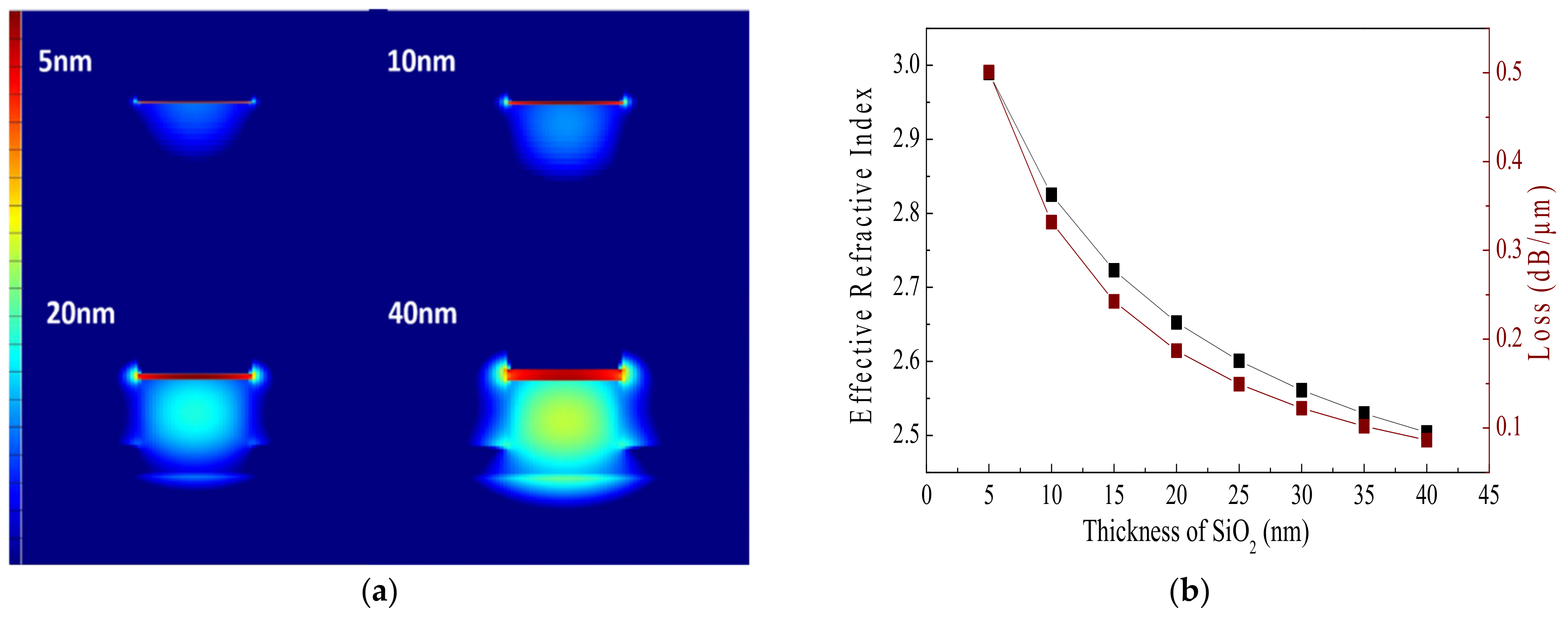
Figure 3a shows the normalized electric field distribution in the plasmonic waveguide (Cu-SiO
2-Si). Note that the plasmonic mode is dominant where the electric field distribution delays an exponential function beyond the SiO
2 layer. As the SiO
2 thickness increases, the mode splits both the plasmonic and the photonic ones gradually. Additionally, the normalized electric field of the photonic mode becomes stronger and the plasmonic one becomes weaker as the oxide layer becomes thicker. Moreover, a thicker SiO
2 layer causes the leaking energy for its poor mode limitation.
Figure 3b shows the effective refractive index (n
eff) and waveguide loss as a function for Cu-SiO
2-Si plasmonic waveguide with SiO
2 thicknesses of 5, 10, 15, 20, 25, 30, 35, and 40 nm, respectively. It can be seen that the n
eff decreases from 2.98 to 2.50, with the SiO
2 thickness increasing from 5 nm to 40 nm, which is explained by the leaking mode. The waveguide loss decreases from 0.5 dB/μm to 0.08 dB/μm, and this decrease is attributed to the mode splitting when more electric fields are in the photonic mode.
The TM mode of the waveguide is coupled into CIPMRMs. For calculating the micro-ring resonant peak intensity, the 3D finite-difference time-domain (FDTD) method is used to calculate the coupling efficiency.
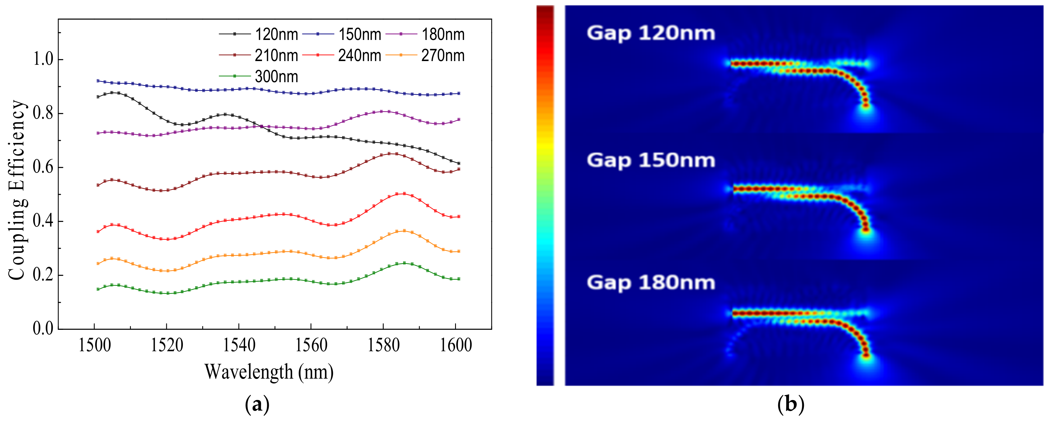
Figure 4a presents the coupling efficiency with different gap distances as the coupling length is 2.53 μm. The coupling efficiency rises first and then falls as the gap decreases from 300 nm to 120 nm. When the gap is 150 nm, the coupling efficiency is at maximum (nearly 90%) because the narrower gap leads the mode to couple back with the waveguide and the wider one causes insufficient coupling, which is represented in
Figure 4b. Moreover, the coupling efficiency curve slightly ascends with the wavelength on the insufficiency coupling condition; the curve descends with the wavelength on the over-coupled condition. The coupling curve is flat when the max coupling efficiency condition is achieved. It implies that the coupling efficiency is affected by the wavelength, especially when the maximum coupling efficiency is not reached. Here, the maximum coupling efficiency is discussed for when the loss of plasmonic micro-ring resonator is −9 dB. To meet the critical coupling condition [
19], where the coupling energy is equal to the micro-ring loss, maximum coupling efficiency (nearly 90%) is needed.
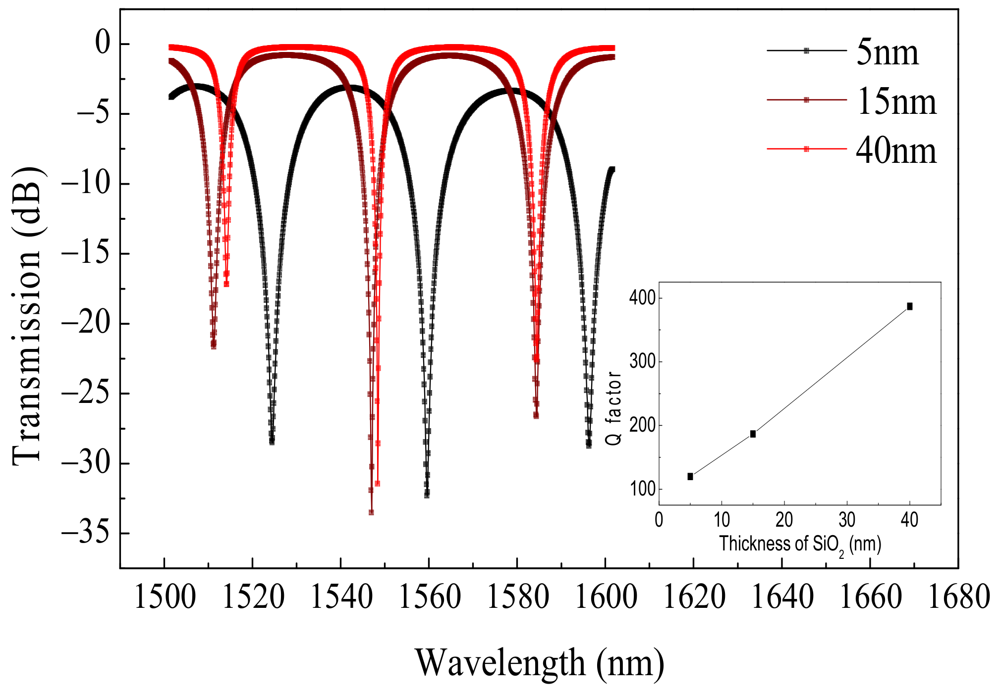
Figure 5 is the transmission curve of the plasmonic micro-ring resonator with different SiO
2 thicknesses. To achieve an excellent extinction ratio (ER), the gap distance is adjusted to meet the requirements of the critical coupling condition. The loss of the plasmonic micro-ring resonator with 15 nm SiO
2 is nearly 3.7 dB. To meet the critical coupling condition, the coupling gap is 210 nm and the coupling efficiency is 58%. The loss of the plasmonic micro-ring resonator with 40 nm SiO
2 is nearly 1.85 dB. To meet the critical coupling condition, the coupling gap is 250 nm and the coupling efficiency is 36% according to the calculation. It can be seen that the resonance peak shifts for different SiO
2 thicknesses. This behavior can be attributed to the change in n
eff for the plasmonic waveguide with different SiO
2 thicknesses. Moreover, the plasmonic waveguide loss (
Figure 3 shows) affects the quality factor (Q) and insertion loss (IL) of the micro-ring. The Q factor increases from 119.9 to 387 and IL decreases from −3.3 dB to −0.3 dB as the thickness of SiO
2 varies from 5 nm to 40 nm.
The high Q factor is a key aim in many fields, such as micro-ring sensors and micro-ring modulators, because it is sensitive to the refractive index change [
20,
21]. It has benefits for modulating, insofar as a slight change in refractive index would shift the resonance peak away from the aiming wavelength. Therefore, it does not consume much energy when low peak-to-peak voltage is applied. However, the side effects of the high Q factor are also obvious for two reasons. First, the high Q factor induces the micro-ring sensitivity to the temperature effects that limit its application. Second, the high Q factor impedes the minority carrier, which causes low bandwidth [
2]. In this work, the plasmonic micro-ring modulator with a low Q factor is discussed to utilize its insensitivity.
4. Temperature Effects on the Carrier-Injection Plasmonic Micro-Ring Modulator
The effect of temperatures on the resonant peak originates from the thermos optical property of silicon, which is 0.000186/K [
22]. The resonant peak shifts 0.11 nm/K as temperature varies, and the temperature changes 1 K are enough to render the device inoperable at the aiming wavelength [
23]. Therefore, heating resistance and temperature control are necessary for the MRMs by thermo-optic resonant tuning [
24]. However, the CIPMRMs we proposed are insensitive to temperature changes due to their low Q factor. Therefore, it needs no complex control circuit for resonant tuning.
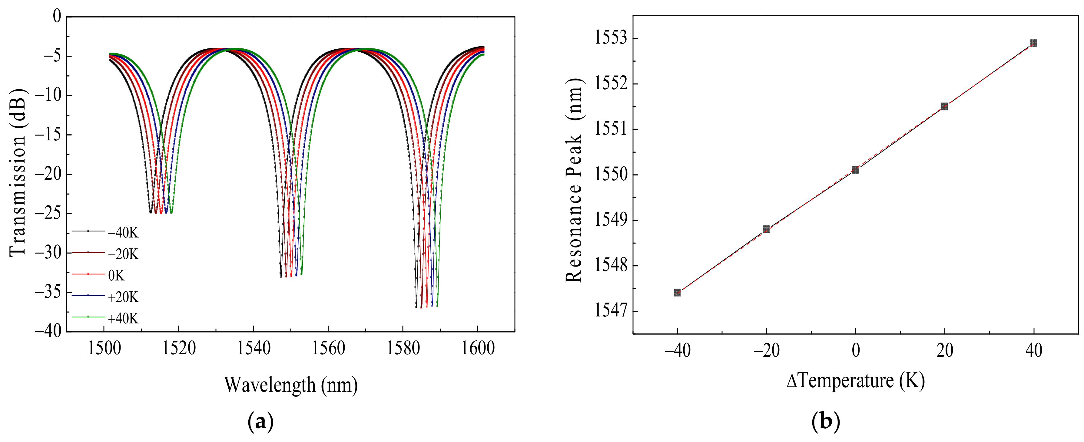
Figure 6a represents the resonant peak of CIPMRMs with 5 nm SiO
2 shifts from 1547.5 nm to 1552.5 nm as temperature varies from 280 K to 360 K. It can be seen that the resonant peak shifting depends on temperature linearly and that the result is 0.075 nm/K (
Figure 6b shows), which is explained by the stable thermos optical coefficient of silicon.
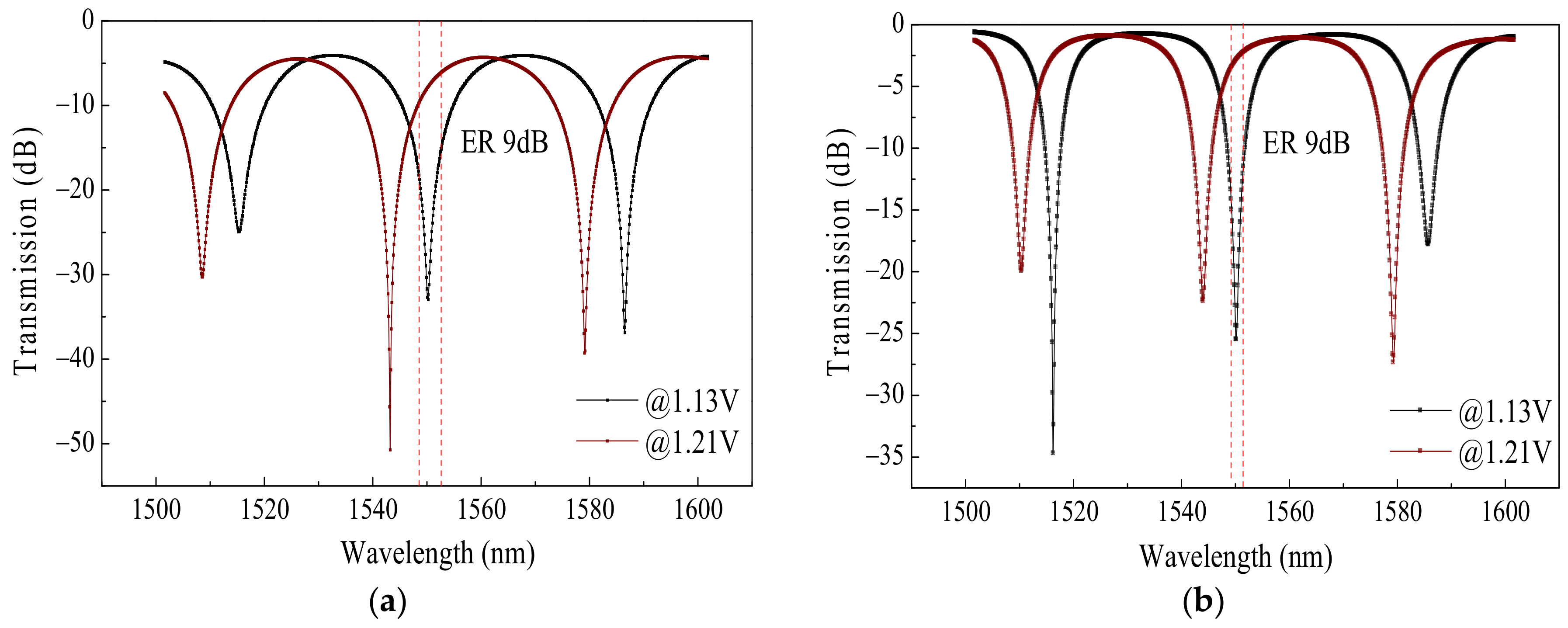
Figure 7a shows the transmission curve of CIPMRM (5 nm SiO
2) on the resonant state (1.13 V) and off the resonant state (1.21 V) at 1550 nm. When the temperature increases, the transmission curve has redshifts. Although the insertion loss rises and the extinction ratio decreases as the transmission curve has redshifted, the plasmonic micro-ring resonator sustains a high extinction ratio during temperature variation. When the temperature decreases, all of the transmission curve have blueshifts. Both the insertion loss and the extinction ratio of CIPMRM decrease. The insertion loss changes slowly, which causes the extinction ratio to decrease with decreases in temperature. The marked wavelength range represents permissible resonant wavelength shifts with temperature variation. We conclude that an ER of 9 dB is satisfied as temperature varies within the 60 K range for CIPMRMs (5 nm SiO
2). The low Q factor promotes stable temperature for the micro-ring modulator. As for the CIPMRM with 40 nm SiO
2, it sustains an ER of 9 dB within 27 K due to its higher Q factor (
Figure 7b).
5. Electrical Stimulation Method
CIPMRMs with 5 nm SiO
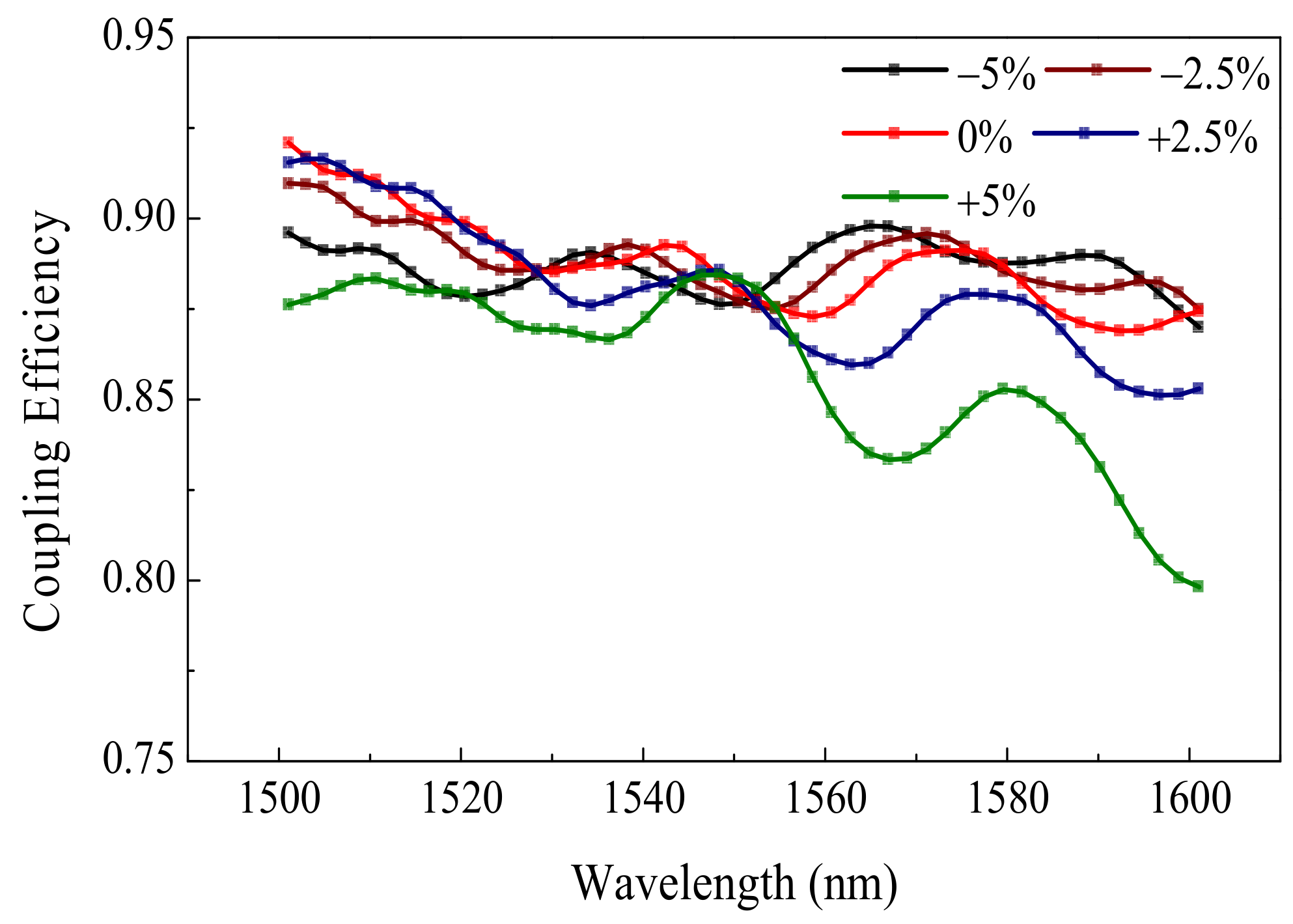
2 are discussed in this section. Expecting that the temperature variation causes the wavelength to shift, another challenge lies in the process error of the linewidth. First, the change in linewidth affects the coupling condition. Increasing the waveguide width binds the mode that impairs the mode coupling. However, increasing the waveguide width also decreases the coupling gap, which tends to improve the mode coupling. Therefore, we conclude that coupling efficiency changes slightly (nearly 85%) with the variation in linewidth (
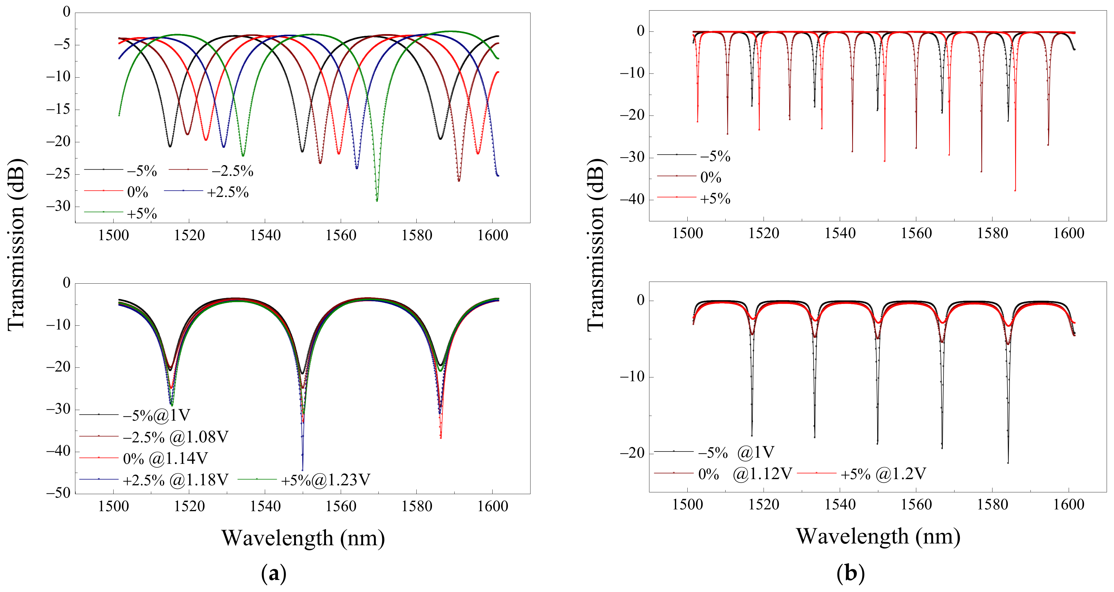
Figure 8). Second, variation in the linewidth is a random process. It causes changes in the refractive index as well as changes in the resonant wavelength. A method of tuning the resonant wavelength by injected carrier concentration is proposed in
Figure 9. To demonstrate this method, plasmonic MRMs and photonic MRMs are compared below. It can be seen that the resonant peak has redshifts from 1550 nm to 1570 nm (plasmonic MRMs) and from 1550 nm to 1570 nm (photonic MRMs) as the width error varies from −5% to 5%. According to the Soref model, the injected carrier that leads to the refractive index decreases, which is utilized for compensating the linewidth error in this work. Therefore, a different voltage is applied for setting the resonant peak at 1550 nm, which is the off-state of the modulator. Changing the voltage shifts the resonant wavelength away from 1550 nm, which represents the on-state of the modulator. Although photonic MRMs can also shift the wavelength back to 1550 nm based on the carrier concentration, they show poor resonance intensity for the effects of the injected carrier on the imaginary part of the refractive index. It follows that the problem of random linewidth (−5%~+5%) is solved by initializing the operating voltage of CIPMRMs, which will promote the yields of CIPMRMs.
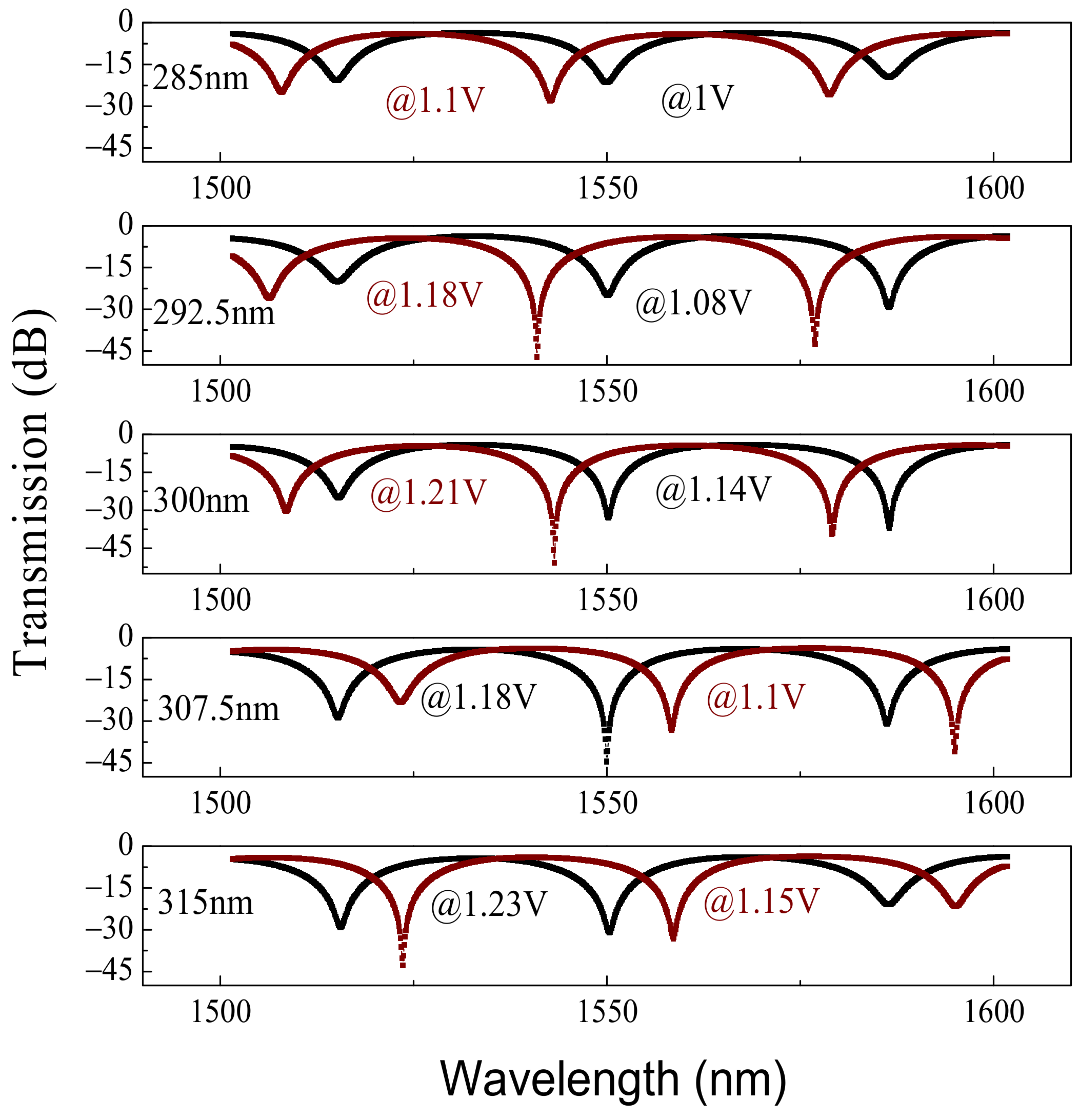
Figure 10 presents the transmission curve of the on-state and the off-state for different linewidths of CIPMRMs. The resonant intensity of the on-state increases with the increasing voltage first and then falls. It is mainly attributed to the increasing micro-ring loss by injected carriers, which are close to the critical coupling condition, and then deviates. The insertion loss varies from −8 dB to −6 dB and the extinction ratio varies from 14 dB to 37.7 dB as linewidth changes from 285 nm to 315 nm.
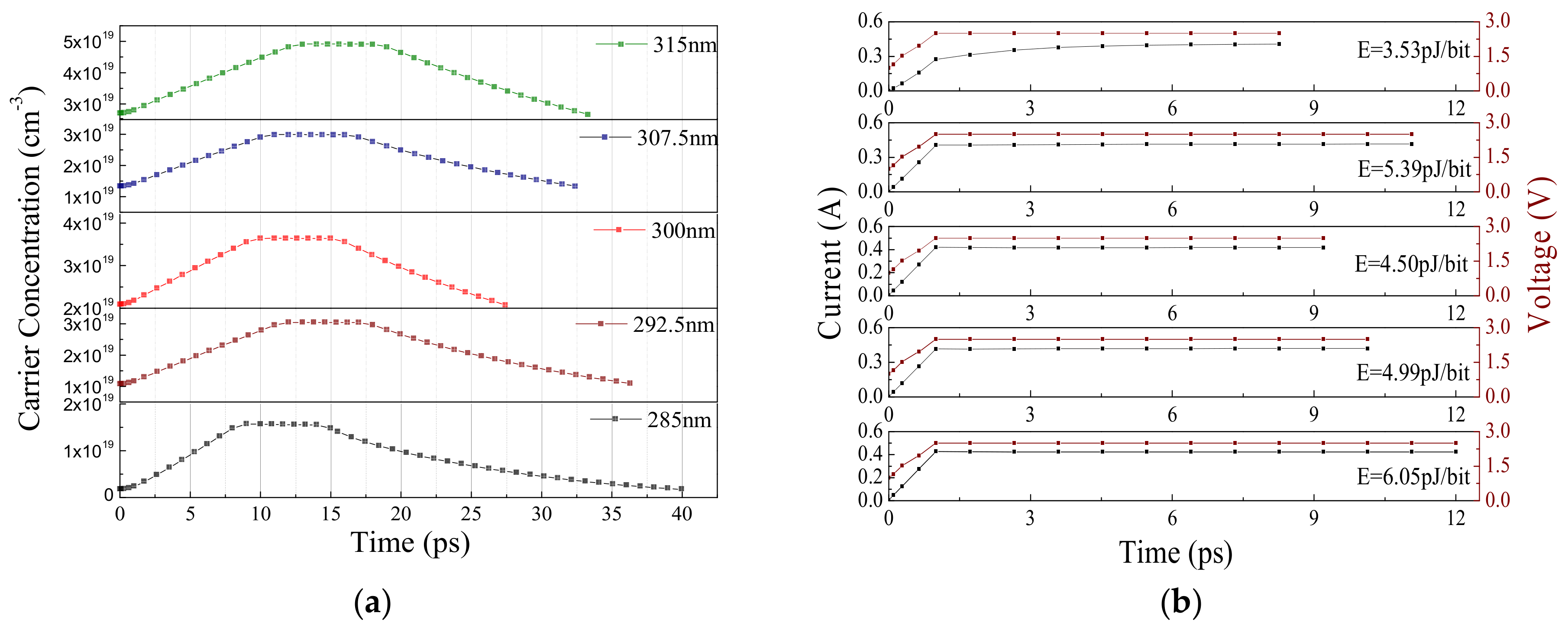
Figure 11a shows the curve of the injected carrier concentration and the time as different voltage conditions are applied for different linewidths of CIPMRMs. To promote the carrier migration, a 2.5 V pre-emphasize voltage is applied for improving the carrier drift velocity. As the carrier concentration achieves the on-state condition, the voltage reduces to the on-state voltage, representing the flat section of the carrier concentration curve. Finally, the voltage decreases to 0 V for releasing the charges of capacitance and then recovers to the off-state voltage as the carrier concentration recovers to the initial state. Bit rate is estimated by the rise and fall times of the carrier concentration, which represents the least amount of time for transporting a bit.
Figure 11b presents the current–time and voltage–time curves. Energy consumption is calculated by
where 1/2 represents the mean energy consumption as “0” bit and “1” bit are transported. One thing worth mentioning here is that static energy consumption is too tiny to be considered. Moreover, there is no energy consumed as capacitance releases the charge. All the results are summarized in
Table 1. Rise time is the linear increase with time that is decided by the carrier concentration of on-state and off-state voltage. The fall time is related to the initial carrier concentration, which leads to the lower bit rate with a 285 nm width. Bit rate is estimated by the carrier transit time (rise time and fall time included), which is the least amount of time needed for transporting a bit. We conclude that the bit rate of CIPMRMs with different widths varies from 28.5 Gbps to 45 Gbps and that the energy consumption of CIPMRMs varies from 3.53 pJ/bit to 6.05 pJ/bit.
Table 2 lists the voltage conditions for different linewidth of CIPMRMs. Using the method of tuning the resonant wavelength based on the carrier concentration, the CIPMRMs work well as the linewidth varies within ±5%. This means the CIPMRMs satisfied by the standard CMOS process initialize the voltage condition, including the bias voltage (V
bias), working point voltage (V
work), pre-emphasize voltage, and its sustained time. After initialization, it works well as temperature changes within 60 K without complex control, and sensor circuit and device.
6. Overview and Conclusions
CIPMRM is a kind of insensitive micro-ring for its huge waveguide loss. By utilizing the low Q of CIPMRMs, the ER is less insensitive to temperature. The micro-rings with low Q are hard to modulate. Therefore, more minority carriers need to be injected. Moreover, the resonant wavelength can be tuned based on the carrier concentration when the linewidth varies. CIPMRMs and the method of tuning the resonant wavelength based on the carrier concentration are first proposed here. Two main issues need to be improved in future work. First, the compensation method for a ±10% variation in linewidth matters, which will boost the yields. Second, the insertion loss of CIPMRMs needs to be improved in future work. If the insertion loss can be reduced to −4 to −6 dB, the performance of CIPMRMs will be comparable with that of photonic MZMs. For MZMs, the energy consumption is only few pJ/bit and the bit rate is 30–50 Gbps (BPSK) [
25,
26,
27]. However, CIPMRMs present a compacted footprint of 43.4 μm
2, which is promising for integration and saving costs.
In summary, a fully CMOS-compatible CIPMRM based on a Cu-SiO2-Si plasmonic waveguide has been proposed and numerically demonstrated. It has a compacted footprint of 43.4 μm2, a data rate of 45 Gbps, an insertion loss of −8 dB, a static extinction ratio of 22 dB, and an energy consumption of 4.5 pJ/bit when 2.5 V peak-to-peak voltage is applied. Due to the low Q of CIPMRMs, an ER of 9 dB is achieved when temperature varies within 60 K. A method of tuning the resonant wavelength based on the carrier concentration is proposed by initializing the voltage condition. Compared with MRMs utilized in the method of tuning the resonant wavelength based on the thermo-optic characteristic of silicon, there is no need for complex temperature control and a feedback circuit. The performances (except IL) of CIPMRMs are comparable with MZMs although it is smaller in size. CIPMRMs provide another technological route for achieving a CMOS-compatible compacted modulator.


