Article

Suppression of Instabilities in a Plasma Voltage Stabilizer

by
Alexander Mustafaev
1,
Artem Grabovskiy
1,* and
Vladimir Sukhomlinov
2
1
Department of General & Technical Physics, Saint Petersburg Mining University, 199106 Saint Petersburg, Russia
2
Department of Optics, Saint Petersburg State University, 199034 Saint Petersburg, Russia
*
Author to whom correspondence should be addressed.
Appl. Sci. 2022, 12(8), 3915; https://doi.org/10.3390/app12083915
Submission received: 23 March 2022 / Revised: 9 April 2022 / Accepted: 12 April 2022 / Published: 13 April 2022
(This article belongs to the Section Applied Physics General)

Abstract

:
This article presents the results of experiments aimed at studying the conditions for the excitation of current and voltage oscillations in plasma in a three-electrode voltage stabilizer. It was found that in the modes under consideration, the plasma had negative conductivity, which caused oscillations. We propose a highly efficient method for suppressing instabilities that is based on controlling the sign of the plasma’s differential conductivity via adjusting the concentration of the plasma’s thermal electrons with an external control electrode. The proposed method makes it possible to achieve a high level of stability of the energy parameters of voltage stabilizers and those of other plasma-based devices.

1. Introduction

One of the key ways to foster the development of industrial facilities and social infrastructure in hard-to-reach regions all over the world is to design small-scale and high-power nuclear reactors that are environmentally friendly [1]. In such designs, it is necessary to use electronic components for current control in reactor circuits. Such components (devices) should work reliably at high radiation levels and ambient temperatures exceeding 1000 K [2]. Semiconductor electronic devices are unable by their nature to meet these requirements [3]. This problem can be solved by means of gas-discharge devices based on nonequilibrium plasma with nonlocal properties [4].
An example of such plasma is a low-voltage beam discharge (LVBD) in inert gases [5]. This type of plasma contains groups of electrons of different energies [6], which can be controlled by additional electrodes, providing more flexibility for modification of plasma properties in desirable ways. This is due to the fact that different energetic groups of electrons are responsible for different processes, and their density modifications yield control over corresponding plasma processes to optimize the energy parameters of plasma devices [7].
This technology can be used in a number of high-tech industries and products, including plasma chemistry, plasma processes applied to different coatings [8], light sources [9], gas analyzers [10,11], and plasma-based devices [12].
Attempts to improve the energy parameters of plasma-energy devices cause plasma instabilities [13,14,15] related to the falling volt–ampere characteristic of the discharge [14,16]. Oscillations and instabilities of this type can be used for practical purposes, but they also have a destructive effect on the energy and electrokinetic parameters of plasma sources and stabilizers. It is obvious that the fight against instabilities should involve controlling the electron velocity distribution function (EVDF) in the operating modes of plasma devices [17,18,19].
Paper [20] studied the electrokinetic parameters of a helium LVBD in a three-electrode device with a control electrode (CE) located outside the interelectrode gap. Such a design made it possible to control groups of electrons of different energies and to identify modes that help to solve the problem of voltage stabilization in the range up to 110 V.
In this article, a device of this type is used to solve the problem of suppressing plasma instabilities by controlling the sign of differential plasma conductivity using an external control electrode.

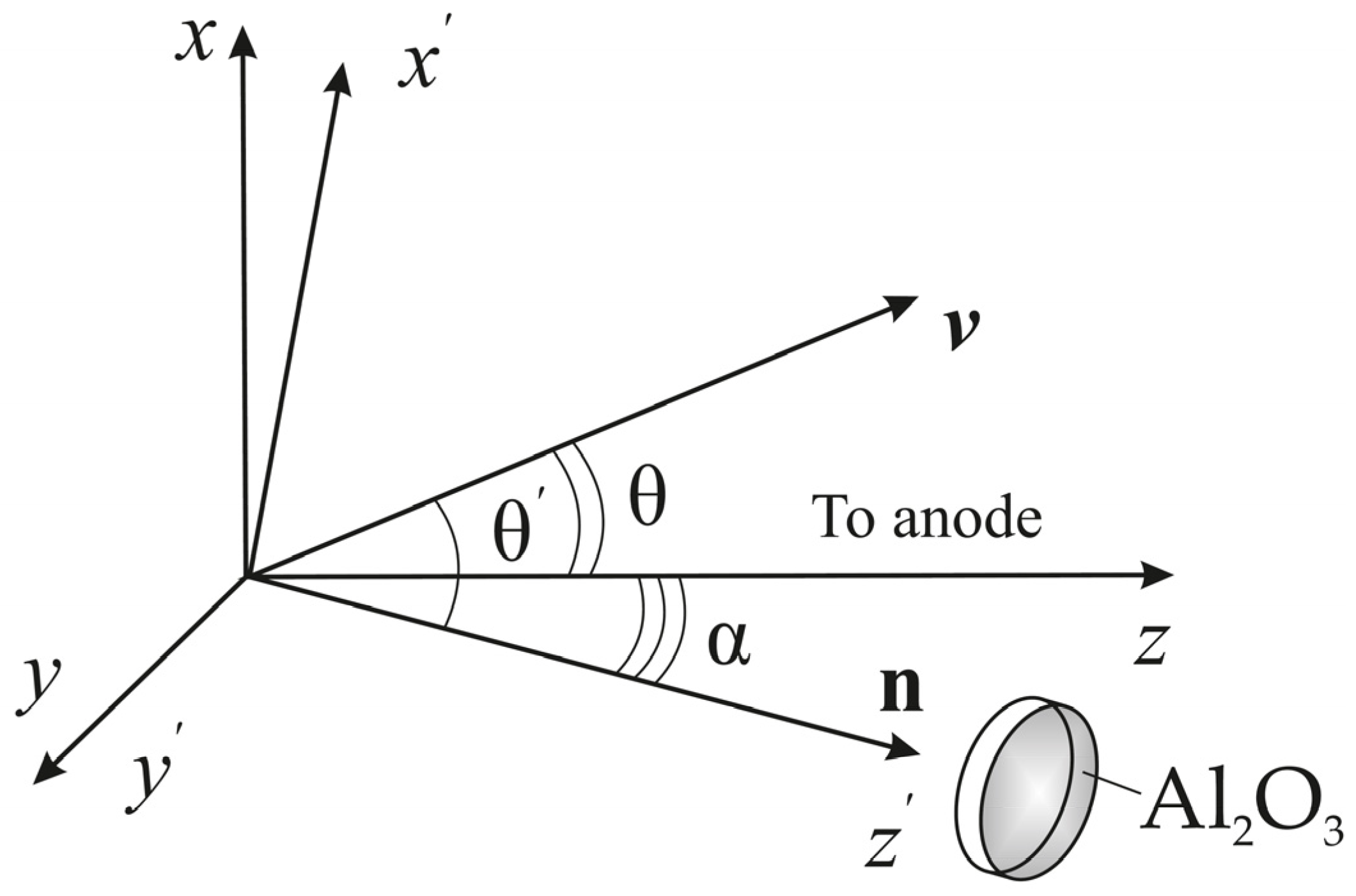
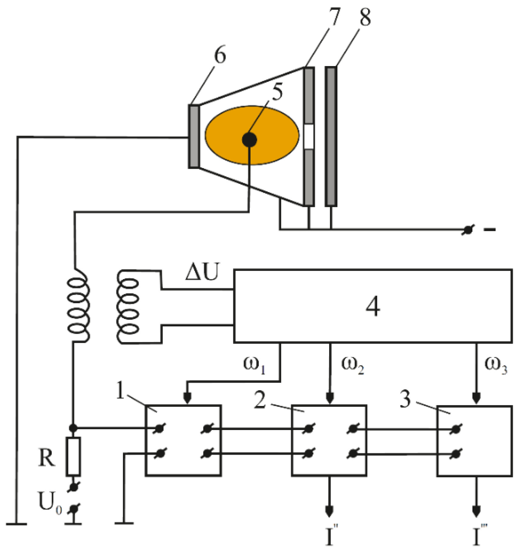
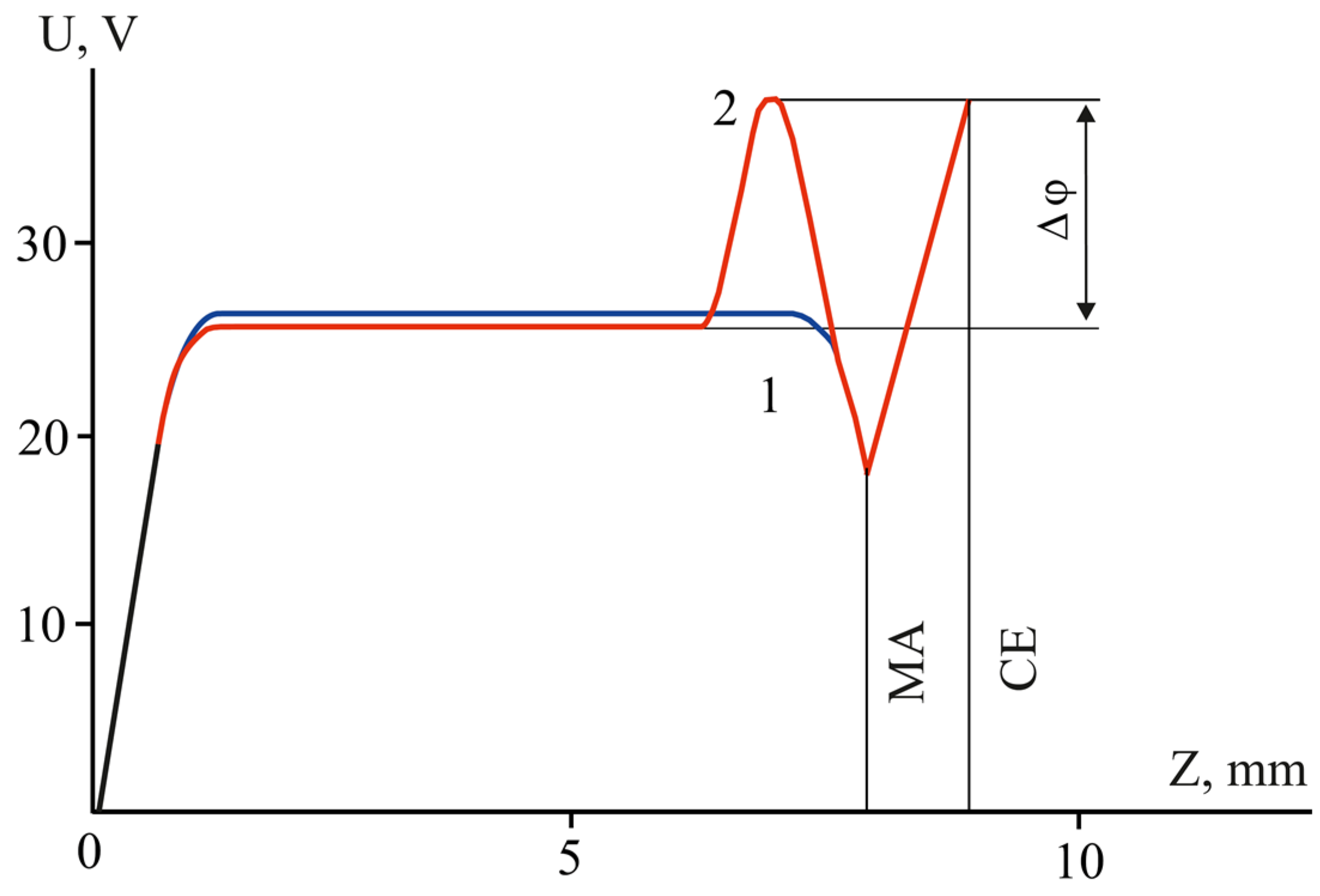
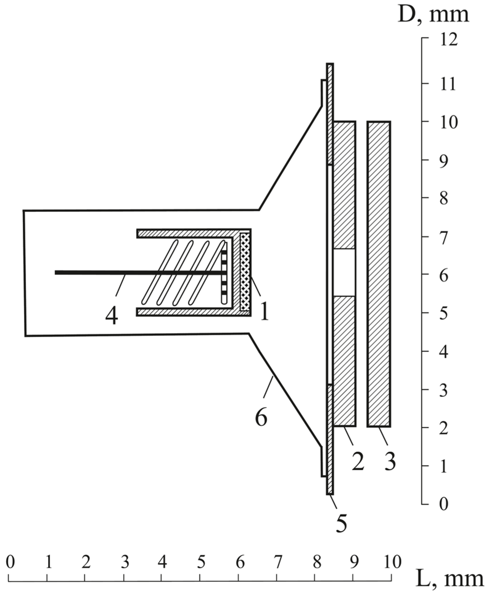
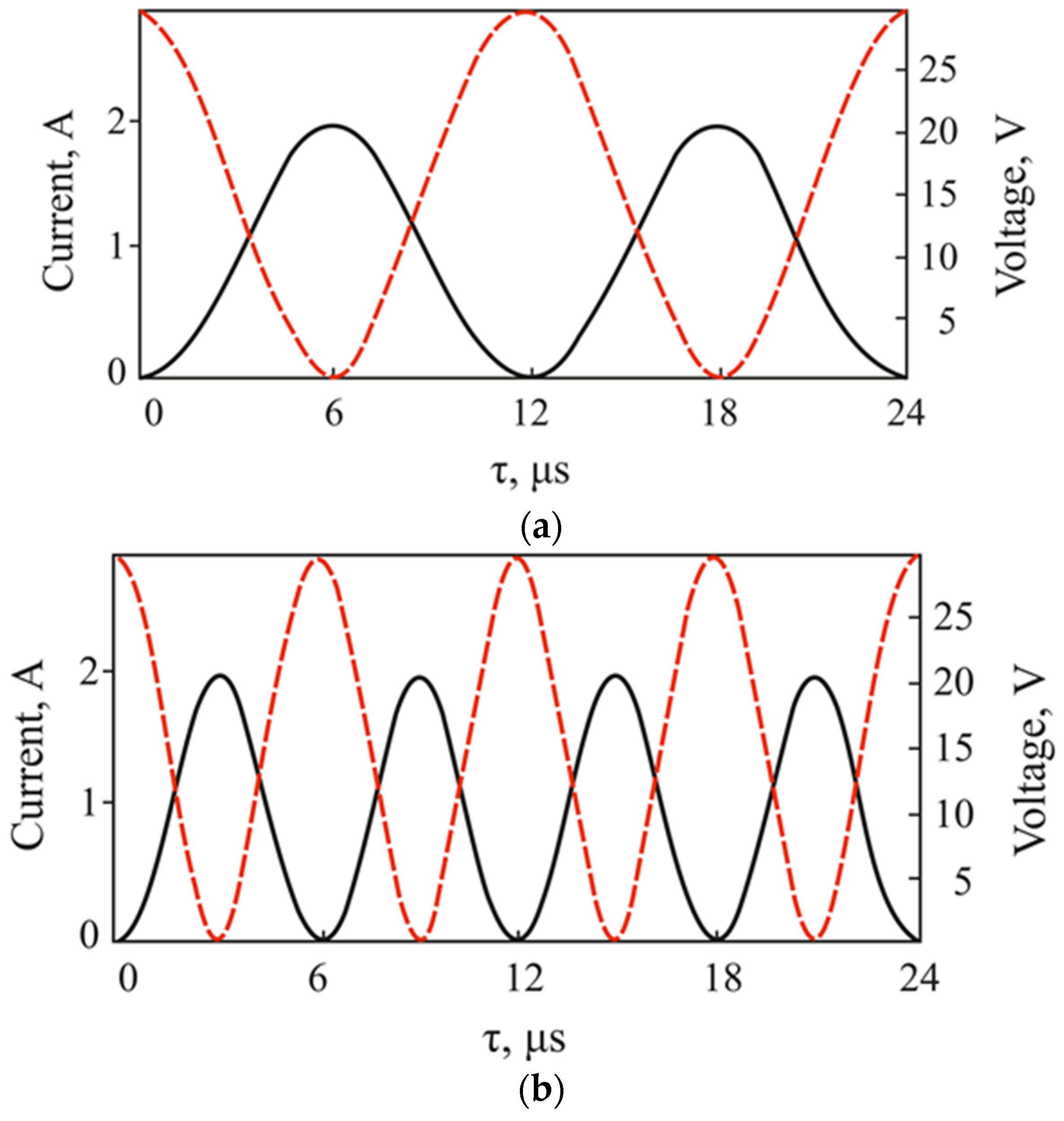
2. Materials and Methods
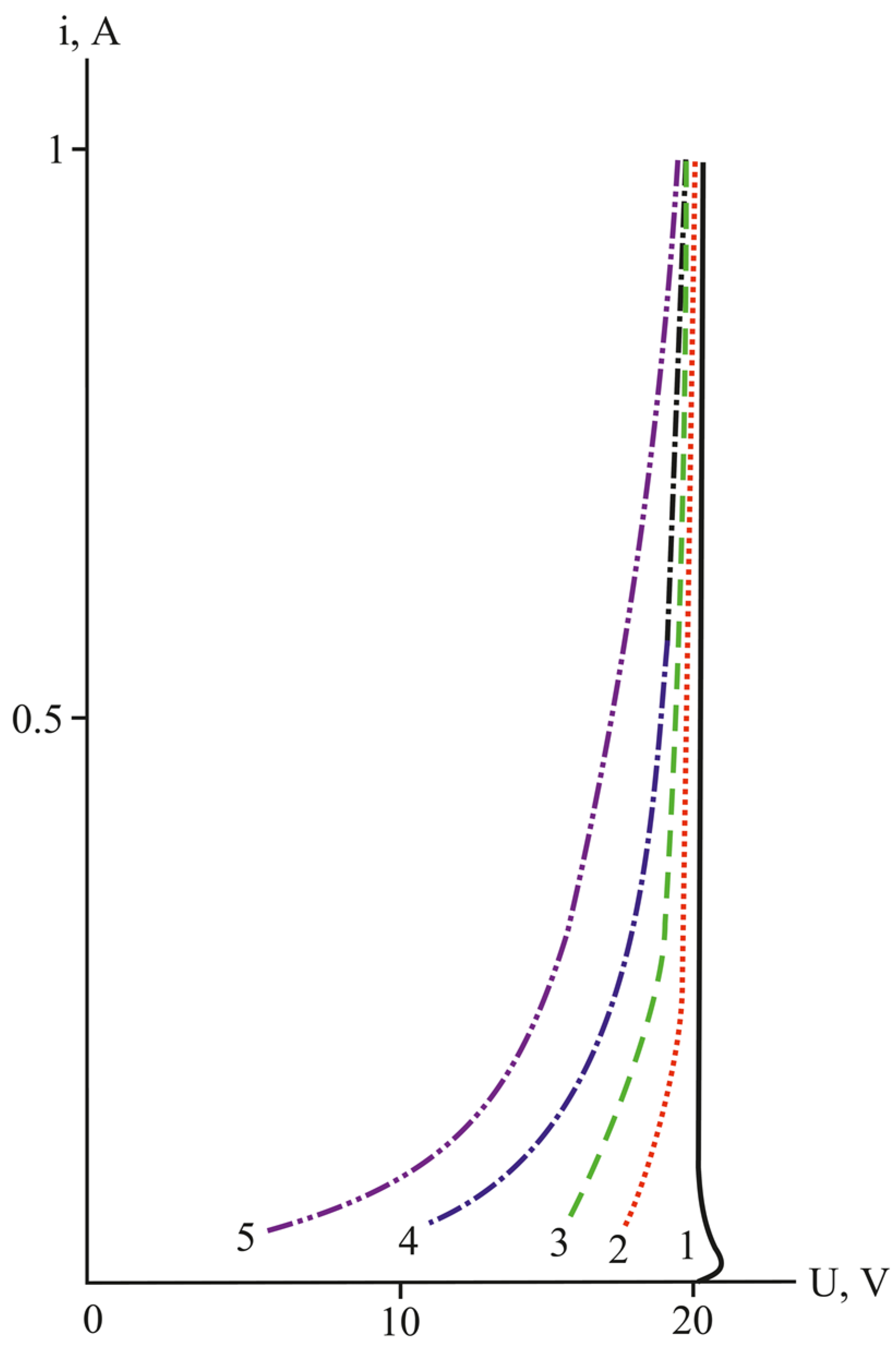
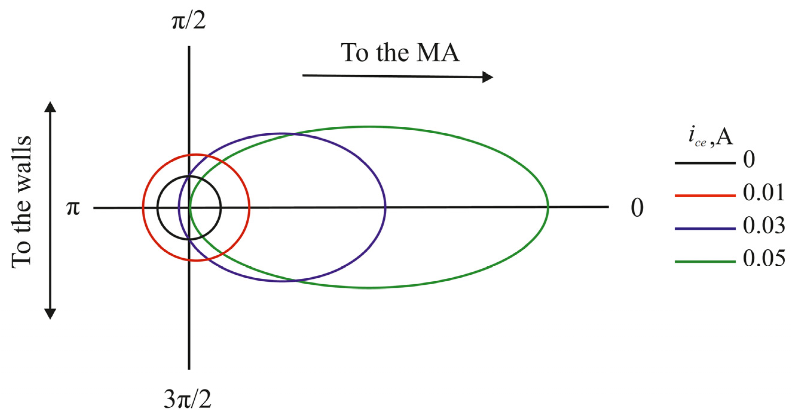
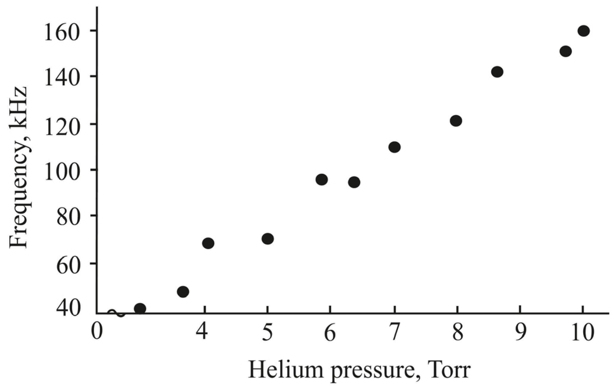
The design of the experimental setup, the design of the triode, and the method for studying plasma are described in detail in [20,21]. Next, we will only describe their key features. Figure 1 shows the diagram of the experimental three-electrode device. The cathode of the device 1 was a tungsten disk impregnated with barium with a diameter of 10 mm. The main anode (MA) 2 and the control electrode 3 were polycrystalline molybdenum discs with a diameter of 30 mm. In the center of the main anode, there was a hole 2 mm in diameter. The control electrode was located at a distance of 1 mm from the main anode outside the discharge zone. The distance between the cathode and the MA was 8 mm. The main element of the heater 4 was a tantalum niobium wire. The plasma discharge channel was limited by a metal conical shield 6, whose potential correlated with that of the cathode.
LVBD investigations were carried out with a method involving a flat, one–sided probe [21]. Since the plasma under the considered experimental conditions demonstrated axial symmetry, the EVDF did not depend on the azimuthal angle (Figure 2):
f ( r ,   v ) = f ( r , v , θ )
where v = | v | , and θ is the polar angle.
The current to a flat Langmuir probe was calculated as
I = q S v n f ( v ) d v = 2 q S m 2 0 2 π d ϕ q U ε d ε 0 θ m a x f ( ε , θ , ϕ ) c o s θ s i n θ d θ
where v n is the component of the electron-velocity vector v , normal to the probe surface, U is the probe potential, ε = m v 2 / 2 , and ϕ and θ are the azimuthal and polar angles of the vector v , respectively. The second derivative of the probe current (2) with respect to the probe potential U is
I U = q 3 S m 2 [ 0 2 π f ( q U , θ = 0 , ϕ ) d ϕ 0 2 π d ϕ q U ( q U ) f ( ε , θ m a x , ϕ ) d ε ] .
Expression (3) can be rewritten as
I U ( q U , α ) = 2 π q 3 S m 2 [ f ( q U , α ) 1 2 π 0 2 π d ϕ q U ( q U ) f ( ε , θ ) d ε ] .
To find the EVDF, we represent f(ε,θ) and I U ( q U , α ) in the form of a series in Legendre polynomials
f ( ε , θ ) = j = 0 f j ( ε ) P j ( c o s θ ) ,
I U ( q U , α ) = 2 π q 3 S m 2 j = 0 F j ( q U ) P j ( c o s α ) .
After substituting (5) and (6) into (4), we obtain the relationship between the components fj and Fj
f ( q U ) = F j ( q U ) + q U f j ( ε ) ( q U ) P j ( q U ε ) d ε .
Expression (7) is a Volterra integral equation of the second kind. Solving it with the resolvent method [22], we obtain
f ( q U ) = F j ( q U ) + q U F j ( ε ) R j ( q U , ε ) d ε .
Let us substitute into Equation (8) the relation
F j ( q U ) = ( 2 j + 1 ) m 2 4 π q 3 S 1 1 I U ( q U , x ) P j ( x ) d x .
and obtain the basic equation to reconstruct the components of fj:
f j ( q U ) = ( 2 j + 1 ) m 2 4 π q 3 S 1 1 [ I U ( q U , x ) + q U I U ( ε , x ) R j ( q U , ε ) d ε ] P j ( x ) d x .
Here, x is the angular variable of the second derivative Legendre polynomials.
Thus, for plasma diagnostics with the flat-probe method, it is necessary to register the values I U ( q U , α ) at various angles of the probe relative to the discharge axis, to calculate a number of Legendre components using (9), and to reconstruct the EVDF according to (5). Equation (9) demonstrates that the method does not require a priori information about the anisotropy of the distribution of charged particles; however, a large number of components is required for a correct description of the EVDF in a strongly non-equilibrium plasma. This is not always possible in a real experiment.
The flat probes were made using a special technology: Tantalum foil at 30-µm-thick was used to die-stamp probes with a diameter of 0.5 mm. Holders made of tantalum wire with a diameter of 0.1 mm were welded to these probes using spot welding. The holder and one of the sides of the probe were covered with alundum paste, and the insulating coating was then sintered in a vacuum at a temperature of 1800 K. The finished probe was mounted on a special three-coordinate micrometer system [21], which made it possible to smoothly change the orientation of the probe relative to the discharge axis.
To measure the second derivative of the probe current and to process the experimental data, a PC-based measuring and computing system was used. We will limit ourselves to a brief description of the principles of experimental data registration.
Figure 3 shows the measurement design. DC voltage was fed to the probe from a controlled DC voltage source. A 100% modulated voltage Δ U = U 0 ( 1 + c o s ω 1 t ) c o s ω 2 t was used as a differentiating signal [21,23], which was fed from the generator through a transformer into the probe circuit. The frequency ω 1 was 1 kHz, and the frequency ω 2 was 100 kHz. The signal was fed to the input of a narrow-band amplifier. The amplified signal was fed to the synchronous detector. The signal of the second derivative of the probe current and the constant voltage of the probe were recorded by digital voltmeters and transferred to a PC.
To measure the EVDF in absolute terms, the probe unit was calibrated. Separately, the circuit was tested for linearity in a wide range of amplitude changes in the differentiating signal.
We shall note that the use of a flat probe requires careful consideration of all factors affecting the accuracy of probe measurements (instrumental effects, probe dimensions, ion current, probe circuit resistance, probe surface contamination, plasma potential oscillations, etc.).
The influence of instrumental effects. To improve both the sensitivity of the method and the signal–to–noise ratio, it was necessary to increase the amplitude of the differentiating signal, which in turn could cause distortion of the real values of the second derivative. In the range of discharge conditions under consideration, the useful signal created by the probe electron current greatly exceeded the noise level, which made it possible to make measurements with a differentiating signal amplitude not exceeding 0.2 V and to consider the hardware distortion to be insignificant. In modes with a much lower value of the useful signal, the instrumental function was used [23].
Ion current. To measure the EVDF, the study used a flat one-sided probe, whose ion current, as is known from [24], was almost independent on the probe potential.
Probe circuit resistance. In the work under consideration, the influence of the resistance of the probe circuit was taken into account and corrected according to the experimental methods described in [23,24].
Plasma potential oscillations. Accounting for the effect of oscillations in the plasma potential was performed by conducting measurements with the differentiating signal turned off. In this case, the distortions caused by oscillations can be found as the ratio of the amplitude of the harmonic being measured without the differentiating signal (i.e., oscillations in the plasma potential only) to the amplitude of the harmonic being measured with the differentiating signal turned on (i.e., including oscillations in the plasma potential).
Probe dimensions. In our case, the problem was solved by strict adherence to the specifications. To do this, the probe was made using a special technology described above.
Probe surface contamination. To avoid the influence of organic vapors, an oil-free turbomolecular pump was used. The probe was cleaned with an ion current with a potential that was negative relative to the plasma. During ion bombardment, the supplied negative potential should not exceed 50 to 100 V. Otherwise, overheating and changes in probe dimensions are possible.

3. Results

In the experiment, the role of the plasma-forming component was played by helium, since it had the highest ionization and excitation potentials among other inert gases. This helps the nonlocal effects in plasma to manifest themselves most clearly. The experiments were carried out at currents of 0.1 to 2 A and helium pressures of 0.1 to 10 Torr. Such conditions were chosen because a plasma can transfer to both local and nonlocal modes. In the latter case, the relaxation lengths for electron–electron Lee and electron–atom Lea collisions exceeded the length of the interelectrode gap d [25].
It is well known that the EVDF in a beam-discharge plasma is formed by two separate groups of electrons, thermal ft and fast beam f0 electrons, with concentrations and average energies of n t , ε ¯ t and n 0 , ε ¯ 0 , respectively [5,7,20]. The velocity distribution of thermal electrons is close to an isotropic Maxwellian one, while the group of fast electrons is characterized by significant anisotropy of the distribution. Comparison of the energies of thermal and beam electrons revealed a strong nonequilibrium of the EVDF; the energy of thermal electrons was about 2 eV, and the energy of fast electrons was about 25 eV.
Such an EVDF shape is a result of the potential distribution over the interelectrode gap. If the current at the main anode is zero, the potential distribution is typical for LVBD (Figure 4, curve 1). There was a potential drop at the anode φ a 1.5 ε ¯ t , which is an almost insurmountable barrier for thermal plasma electrons. The electrons emitted by the cathode were accelerated by the near-cathode sheath and formed a beam with a small energy scatter that went through the interelectrode gap. The creation of thermal electrons occurred as a result of the ionization of helium atoms by the beam electrons. The excitation and ionization potentials for He were Um ≈ 19.8 V and Uion ≈ 24.6 V, respectively; they determine the dominant role of the beam in inelastic processes and current transfer [6,7,20].
In order to study the processes occurring in the plasma conditions under consideration, the Legendre components of the EVDF decomposition f0f6 were reconstructed based on the recorded values of I U ( q U , α ) , which determine the set of the most important plasma parameters: concentration, electron current density, electron pressure anisotropy, etc. [21]. In particular, the function of atomic excitation and ion generation using the component f0 can be calculated as
G = 4 π N a v t r v σ e a i ( v ) f 0 ( v ) v 2 d v ,
where σ e a i is the energy dependence of the cross-section of the corresponding process, and v is the velocity of the incident electron.
As already mentioned, an LVBD can be unstable with the excitation of various types of oscillations [13,14,15,25,26] that negatively affect the operating modes of plasma electronic devices.
Figure 5 shows the current–voltage curves of the helium LVBD recorded for a three-electrode voltage stabilizer. Curve 1 demonstrates the negative differential conductivity that causes oscillations of the discharge current and voltage [14,16,27].
Figure 6 shows the typical form of such oscillations at different values of helium pressure. They occurred at a full modulation of the current in the discharge at frequencies of 50 to 150 kHz and at peak voltage values reaching 30 V. Under constant pressure conditions, the oscillation frequency changed little with changes in the discharge current. If the current increased, the modulation depth dropped to 10%. With an increase in the vapor pressure, the frequency of oscillations increased almost linearly (Figure 6 and Figure 7).

4. Discussion

Table 1 presents the axial distribution of the plasma parameters before the onset of oscillations. The generation function G (shows the number of ions generated per unit volume in 1 s) was found using (10) and the measured Legendre component of the EVDF f0. The quantity D = n i / τ determines the departure of ions from the plasma channel in the radial direction, where τ ~ r / v ¯ d r is the radial ion diffusion time, and the ion velocity v ¯ d r in a radial field with a strength Er of ~5 V/cm is about 2 × 105 cm/s [28].
It can be seen from the table that D increased slightly with the distance from the cathode in the axial region of the plasma due to an increase in the radial concentration and E-field gradient. At the same time, due to the influence of radial diffusion and inelastic processes, the fast part of the EVDF was depleted. This led to a decrease in the function of the generation of ions G. Near the anode, the values of G and D were comparable (Figure 8), which made it possible to write the stationarity condition of the ion concentration in the form GD. If this condition is violated (at GD), an excess amount of ions forms in the anode region, followed by an increase in the current of thermal electrons to the anode and the onset of relaxation oscillations, the nature of which also depends on the anode load. At GD, a deficiency of ions can lead to current interruption.
Thus, the nature of the onset of oscillations can be understood by considering the relationship between the processes of ion generation in the plasma and the escape of ions from the interelectrode gap. It can be seen from (10) that the generation function increased with an increase in helium pressure, and that the ion diffusion flux to the anode increased (the travel time of ions in the MA–to–cathode gap was in the range of milliseconds, which was in good agreement with the oscillation frequencies). This compensated for the near-anode space charge of thermal electrons previously trapped in the potential well between the cathode and the main anode. As a result, their chaotic current to the MA it will increase. Assuming a zero near-anode potential barrier, the quantity it can be written as
i t = 1 4 e n e v t S
where e is the electron charge, ne is the concentration of electrons near the main anode, vt is the thermal velocity of electrons, and S is the MA surface area. Estimates at PHe = 5 Torr, ne ~1011 cm−3, and Te ~1 eV gave it ~1.8 A, which was close to the recorded values (Figure 6).
Based on the conducted research, a method to suppress current and voltage oscillations was proposed [29]. If we consider the gap between the main anode and the control electrode, the hole in the anode acts as a plasma cathode and the current transfer here is carried out mainly by thermal electrons from the plasma in the cathode–MA gap. This becomes possible due to their acceleration caused by a potential jump ∆φ of the double layer near the anode (Figure 4, curve 2). The formation of double layers near the narrowing of the discharge channel has been known for a long time [30] and has been well studied [31,32].
Based on probe measurements, the EVDF was reconstructed and its angular structure was analyzed. Figure 9 shows an increase in the degree of anisotropy of thermal electrons accelerated by a strong electric field near the anode hole. The degree of anisotropy increased as the current at the CE increased. This means that thermal electrons, which were previously locked in the potential well between the cathode and the MA, began to participate in the process of current transfer in the MA–CE gap.
As slow electrons become involved in current transfer, it is possible to influence the balance in the concentration of charged particles in the main gap of the device. Figure 5 shows that sending the current of thermal electrons to the control electrode makes it possible to control the sign of differential conductivity. Carrying out such control allows for the effective suppression of current and voltage oscillations, which is illustrated by the fact that no oscillations occurred in any of the modes with positive differential conductivity (Figure 5, curves 2–5).

5. Conclusions

The article presents the results of probing studies of the EVDF and the distribution of parameters in the beam plasma of a three-electrode voltage stabilizer. It showed that the plasma contained two groups of electrons of different energies and concentrations: fast beam electrons and thermal plasma electrons. Oscillations of the discharge current and voltage were observed at helium pressures of 1 to 10 Torr. It was found that the I–V curve of the device demonstrated a negative differential conductivity that caused the instability. The ion generation function G and the quantity D, which determine ion departure from the plasma channel, were calculated based on data from probe measurements. It was revealed that the onset of oscillations was caused by violating the condition GD. A method for the suppression of oscillations was developed. It consisted of controlling the sign of the differential conductivity of the plasma by sending thermal electrons to the control electrode. The proposed method provided a high level of stability of the operating parameters of high-voltage [20] and low-voltage [33] gas-discharge stabilizers and other plasma devices with various types of control electrodes: non-flat electrode with holes [33], wall grooves [34], an auxiliary electrode [35,36] or an auxiliary electrode with a hole [37].
Research in this field is also crucial for the development of plasma technologies, which are used in industrial and extractive industries, for example, in metallurgy [38,39,40,41], oil production [42], and synthesis of composite materials [43].

Author Contributions

Conceptualization, methodology, V.S.; formal analysis, investigation, A.G.; data curation, writing—review and editing, supervision, project administration, A.M. All authors have read and agreed to the published version of the manuscript.

Funding

The work was supported by the Russian Science Foundation (RSF), the grant No 21-19-00139.

Institutional Review Board Statement

Not applicable.

Informed Consent Statement

Not applicable.

Data Availability Statement

The data presented in this study are available in the article. Initial experimental data are available on request from the corresponding author.

Conflicts of Interest

The authors declare no conflict of interest.

References

  1. Ivanov, S.V.; Kuznetsov, V.I. Development of energy strategy for the Arctic and regions of the Russian Federation Far North until 2030. In Proceedings of the VI International Conference Arctic 2021, Moscow, Russia, 3–4 March 2021; pp. 10–13. [Google Scholar]
  2. Krotov, A.D.; Lazarenko, G.E.; Ovcharenko, M.K.; Pyshko, A.P.; Sonko, A.V.; Yarygin, V.I.; Lazarenko, D.G. Autonomous thermal emission nuclear power plant for offshore gas and oil platforms. Izv. Vuzov. Yad. Energ. 2011, 3, 21–27. [Google Scholar]
  3. Jiménez, C.M.; Stankovic, N.; Vannier, J.-C.; Shklyarskiy, Y.E.; Bardanov, A.I. Multi-terminal dc grid overall control with modular multilevel converters. J. Min. Inst. 2020, 243, 357–370. [Google Scholar] [CrossRef]
  4. Tsendin, L.D. Nonlocal electron kinetics in gas-discharge plasma. Phys. Uspekhi 2010, 53, 133. [Google Scholar] [CrossRef]
  5. Baksht, F.G.; Lapshin, V.F. Vliyanie neuprugih stolknovenij na strukturu energeticheskogo spektra bystryh elektronov v nizkovol’tnom puchkovom razryade v gelii [Effect of inelastic collisions on the structure of the energy spectrum of fast electrons in a low-voltage beam discharge in helium]. J. Tech. Phys. 1991, 61, 13–18. [Google Scholar]
  6. Kolobov, V.I.; Tsendin, L.D. Analytic model of the cathode region of a short glow discharge in light gases. Phys. Rev. A 1992, 46, 7837. [Google Scholar] [CrossRef]
  7. Adams, S.F.; Demidov, V.I.; Bogdanov, E.A.; Koepke, M.E.; Kudryavtsev, A.A.; Kurlyandskaya, I.P. Control of plasma properties in a short direct-current glow discharge with active boundaries. Phys. Plasmas 2016, 23, 024501. [Google Scholar] [CrossRef]
  8. Al-Bataineh, S.A.; Szili, E.J.; Gruner, P.J.; Priest, C.; Griesser, H.J.; Voelcker, N.H.; Steele, D.A. Fabrication and operation of a microcavity plasma array device for microscale surface modification. Plasma Processes Polym. 2012, 9, 638–646. [Google Scholar] [CrossRef]
  9. Higashiguchi, T.; Terauchi, H.; Otsuka, T.; Yamaguchi, M.; Kikuchi, K.; Yugami, N.; O’Sullivan, G. Microdischarge extreme ultraviolet source with alkali metal vapor for surface morphology application. J. Appl. Phys. 2011, 109, 013301. [Google Scholar] [CrossRef]
  10. Eun, C.K.; Gianchandani, Y.B. Microdischarge-based sensors and actuators for portable microsystems: Selected examples. IEEE J. Quantum Electron. 2012, 48, 814–826. [Google Scholar] [CrossRef]
  11. Demidov, V.I.; Adams, S.F.; Blessington, J.; Koepke, M.E.; Wiliamson, J.M. Short dc discharge with wall probe as a gas analytical detector. Contrib. Plasma Phys. 2010, 50, 808–813. [Google Scholar] [CrossRef]
  12. Chen, K.F.; Eden, J.G. The plasma transistor: A microcavity plasma device coupled with a low voltage, controllable electron emitter. Appl. Phys. Lett. 2008, 93, 161501. [Google Scholar] [CrossRef]
  13. Stefanović, I.; Kuschel, T.; Škoro, N.; Marić, D.; Petrović, Z.L.; Winter, J. Oscillation modes of direct current microdischarges with parallel-plate geometry. J. Appl. Phys. 2011, 110, 083310. [Google Scholar] [CrossRef] [Green Version]
  14. Raizer, Y.P. Gas Discharge Physics; Springer: New York, NY, USA, 1997; 463p, ISBN 0-387-19462-2. [Google Scholar]
  15. Phelps, A.V.; Petrović, Z.L.; Jelenković, B.M. Oscillations of low-current electrical discharges between parallel-plane electrodes. III. Models. Phys. Rev. E 1993, 47, 2825. [Google Scholar] [CrossRef] [PubMed]
  16. Kaganovich, I.D.; Fedotov, M.A.; Tsendin, L.D. Ionization instability of a Townsend discharge. J. Tech. Phys. 1994, 39, 241–246. [Google Scholar]
  17. Denisov, V.V.; Akhmadeev, Y.H.; Koval, N.N.; Kovalsky, S.S.; Lopatin, I.V.; Ostroverkhov, E.V.; Schanin, P.M. The source of volume beam-plasma formations based on a high-current non-self-sustained glow discharge with a large hollow cathode. Phys. Plasmas 2019, 26, 123510. [Google Scholar] [CrossRef]
  18. Korotkov, S.V.; Zhmodikov, A.L. A High-Power Diode–Dynistor Generator for Gas-Discharge Technologies. Instrum. Exp. Tech. 2021, 64, 683–686. [Google Scholar] [CrossRef]
  19. Zhong, S.; Qin, F.; Gao, Y.; Yan, Z. Response Characteristics of Gas Discharge Tube to High-Power Microwave. IEEE Access 2021, 9, 111486–111492. [Google Scholar] [CrossRef]
  20. Mustafaev, A.; Grabovskiy, A.; Krizhanovich, A.; Sukhomlinov, V. Beam-Plasma Stabilizer for the New Type of Nuclear Power Energy Systems. Appl. Sci. 2021, 11, 11419. [Google Scholar] [CrossRef]
  21. Mustafaev, A.S.; Grabovskiy, A.Y. Probe Diagnostics of Anisotropic Electron Distribution Function in Plasma. High Temp. 2012, 50, 785–805. [Google Scholar] [CrossRef]
  22. Volterra, V. Theory of Functionals and of Integral and Integro-Differential Equations; Dover Publications: New York, NY, USA, 1930; 288p, ISBN 978-048-644-284-6. [Google Scholar]
  23. Demidov, V.I.; Kolokolov, N.B.; Kudryavtsev, A.A. Zondovye Metody Issledovaniya Nizkotemperaturnoj Plazmy [Probe Methods for Studying Low-Temperature Plasma]; Energoatomizdat: Moscow, Russia, 1996; 235p, ISBN 5-283-03927-7. [Google Scholar]
  24. Ovsyannikov, A.A.; Engelsht, V.A.; Lebedev, Y.A. Diagnostika Nizkotemperaturnoi Plasmi [Diagnosis of Lowtemperature Plasma]; Nauka: Novosibirsk, Russia, 1994; p. 483. ISBN 5-02-030197-3. [Google Scholar]
  25. Kharchenko, I.F.; Fainberg, Y.B.; Kornilov, E.A. Interaction of an electron beam with a plasma in a magnetic field. Zh. Tekh. Fiz. 1961, 31, 761. [Google Scholar]
  26. Kornilov, E.A.; Kovpik, O.F.; Fainberg, Y.B. Mechanism of plasma formation during the development of beam instability. Zh. Tekh. Fiz. 1965, 35, 1378. [Google Scholar]
  27. Garyainov, S.L.; Abezgauz, I.D. Poluprovodniki s Otricatel’nym Soprotivleniem [Negative Resistance Semiconductors]; Energiya: Moscow, Russia, 1970; 320p. [Google Scholar]
  28. Zakharova, V.M.; Kagan, Y.M. On the motion of ions and atoms in plasma. Spektrosk. Gazorazryadnoi Plazmy 1970, 1, 291–318. [Google Scholar]
  29. Mustafaev, A.S.; Grabovskiy, A.Y. Method for Stabilizing Electrical Parameters in Gas-Discharge Devices with Negative Resistance. RF Patent 2498441, 10 November 2013. [Google Scholar]
  30. Wasserab, T. Two-layer voltage of low-pressure gas discharges. J. Appl. Phys. 1963, 16, 454–460. [Google Scholar]
  31. Gryaznevich, M.P.; Lavrov, B.P. Aksial’noe raspredelenie osnovnyh parametrov plazmy tleyushchego razryada s suzheniem v gelii [Axial distribution of the main parameters of a glow discharge plasma with constriction in helium]. PZhTF 1977, 3, 697–700. [Google Scholar]
  32. Lavrov, B.P.; Simonov, V.Y. O sloyah ob’emnogo zaryada v prianodnoj plazme mono- i duoplazmatronov [On space charge layers in near-anode plasma of mono- and duoplasmatrons]. JTF 1978, 48, 1744–1746. [Google Scholar]
  33. Mustafaev, A.S.; Grabovskiy, A.Y. Low-voltage beam discharge in light inert gases to solve problems of voltage stabilization. High Temp. 2017, 55, 24–30. [Google Scholar] [CrossRef]
  34. Li, H.; Ning, Z.; Yu, D. Hall thruster with grooved walls. Appl. Phys. 2013, 113, 083303. [Google Scholar] [CrossRef]
  35. Strat, M.; Strat, G.; Gurlui, S. Basic processes in discharge plasma double layer. J. Phys. D Appl. Phys. 1999, 32, 34. [Google Scholar] [CrossRef]
  36. Ionita, C.; Dimitriu, D.G.; Schrittwieser, R.W. Elementary processes at the origin of the generation and dynamics of multiple double layers in DP machine plasma. Int. J. Mass Spectrom. 2004, 233, 343–354. [Google Scholar] [CrossRef]
  37. Demidov, V.I.; DeJoseph, C.A.; Simonov, V.Y. Gas-discharge plasma sources for nonlocal plasma technology. Appl. Phys. Lett. 2007, 91, 201503. [Google Scholar] [CrossRef]
  38. Baake, E.; Shpenst, V.A. Recent scientific research in the field of electrothermal metallurgical processing. J. Min. Inst. 2019, 240, 660–668. [Google Scholar] [CrossRef] [Green Version]
  39. Matveeva, V.; Lytaeva, T.; Danilov, A. Application of steel-smelting slags as material for reclamation of degraded lands. J. Ecol. Eng. 2018, 19, 97–103. [Google Scholar] [CrossRef]
  40. Gulkov, Y.V.; Turysheva, A.V.; Vinogradova, I.V. Producing steels with special properties using a jet heat treatment system. Key Eng. Mater. 2020, 854, 30–36. [Google Scholar] [CrossRef]
  41. Martynov, S.A.; Bazhin, V.Y.; Petrov, P.A. A digital control system designed for ore thermal furnaces producing metallurgical silicon. Tsvetnye Met. 2021, 2021, 70–76. [Google Scholar] [CrossRef]
  42. Maksyutin, A.V.; Khusainov, R.R. Results of experimental researches of plasma-pulse action technology for stimulation on the heavy oil field. World Appl. Sci. J. 2014, 31, 277–280. [Google Scholar] [CrossRef]
  43. Ermakov, S.B.; Vologzhanina, S.A.; Ermakov, B.S. Features of obtaining Ni-Cr-Fe alloy powders by plasma atomization. MSF 2021, 1040, 1–7. [Google Scholar] [CrossRef]
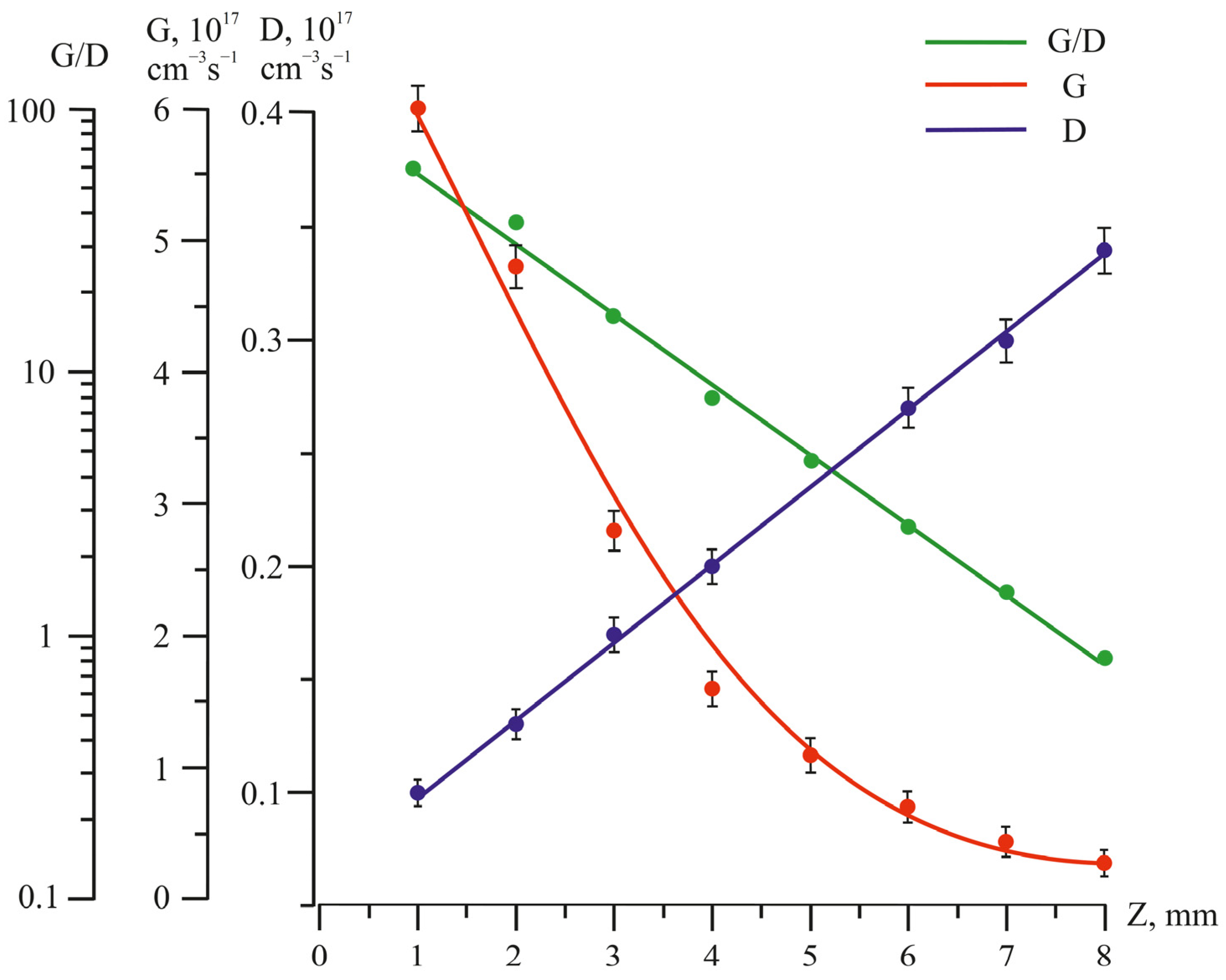
Figure 1. The device with a narrowed discharge channel: cathode (1), main anode (2), external control electrode (3), heater (4), alundum insulators (5), and conductive shield (6).
Applsci 12 03915 g001
Figure 2. Orientation of the probe in the plasma (here, θ is the polar angle of the EVDF in x-y-z coordinate system, θ is the polar angle of the vector v in x′-y′-z′ system, and α is the angle between the normal to the probe surface and the plasma symmetry axis.
Applsci 12 03915 g002
Figure 3. Measurement design: 1–3—synchronous detectors; 4—driving generator; 5—flat one-sided probe; 6—cathode; 7—main anode; and 8—control electrode [21].
Applsci 12 03915 g003
Figure 4. Potential distribution over the gap of the experimental device at helium pressure PHe = 2.5 Torr; currents at the CE ice, A: 1–0; 2–0.04.
Applsci 12 03915 g004
Figure 5. Current–voltage curves of the stabilizer at various CE currents ice, A: 1–0; 2–0.02; 3–0.04; 4–0.06; 5–0.08; PHe = 3 Torr.
Applsci 12 03915 g005
Figure 6. Typical graphs of discharge current (solid curves) and voltage (dashed curves) oscillations: (a) at PHe = 5 Torr; (b) at PHe = 10 Torr.
Applsci 12 03915 g006
Figure 7. Oscillation frequency vs. helium pressure.
Applsci 12 03915 g007
Figure 8. Axial dependences of quantities D (1), G (2), and G/D (3). Here, G is the function of atomic excitation and ion generation; quantity D determines the departure of ions from the plasma discharge channel in the radial direction.
Applsci 12 03915 g008
Figure 9. Angular structure of the thermal electrons’ EVDF near the anode hole for various currents at the CE and PHe = 3 Torr. The horizontal axis coincides with the discharge symmetry axis.
Applsci 12 03915 g009
Table 1. Axial distribution of plasma parameters at PHe = 2 Torr and a discharge current of 0.5 A.
Z, mmφ, Vn0, 109 cm−3nt, 1011 cm−3τ, s D = n i / τ ,   10 17   cm 3   s 1 G, 1017 cm−3 s−1G/D
120.1150.54.00.16.060.0
220.7120.755.50.134.837.0
321.271.237.00.172.816.4
421.441.68.50.21.68.0
5222.742.5100.241.14.58
622.41.753.7311.50.270.72.59
722.81.115.57130.30.441.47
823.30.718.2914.50.340.280.82
Publisher’s Note: MDPI stays neutral with regard to jurisdictional claims in published maps and institutional affiliations.

