
A 19 ps Precision and 170 M Samples/s Time-to-Digital Converter Implemented in FPGA with Online Calibration


Abstract
:1. Introduction
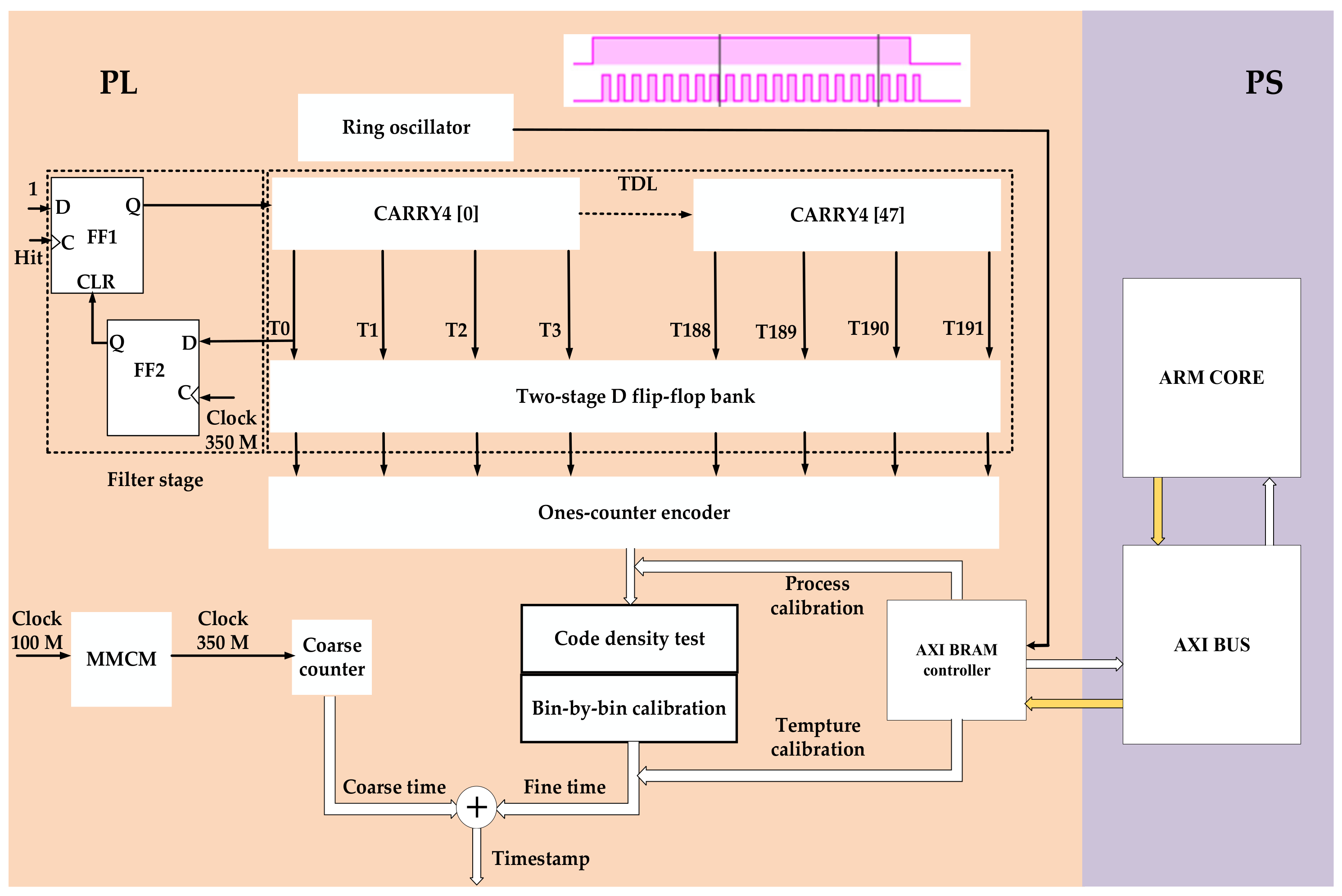
2. TDC Architecture
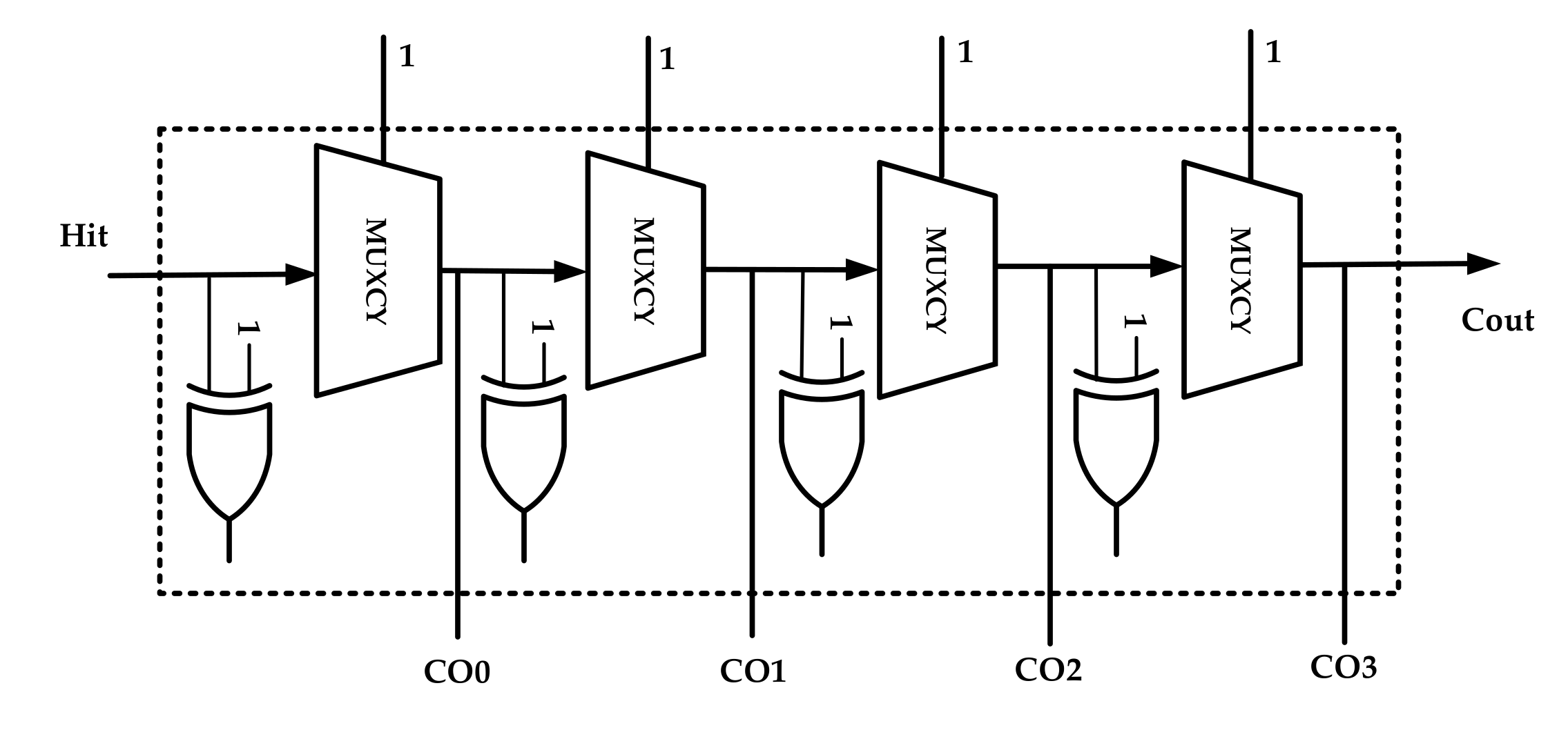
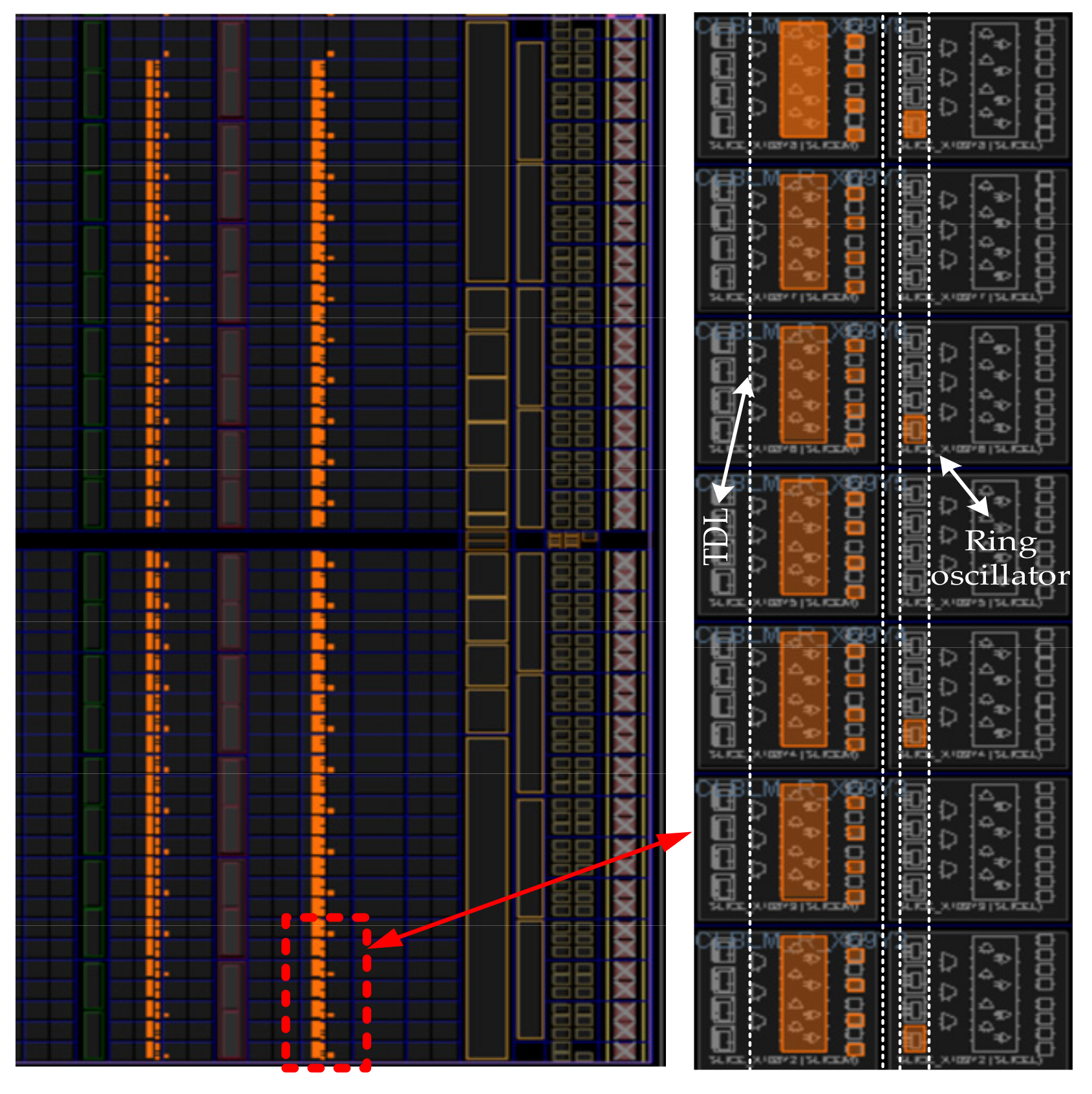
2.1. Tapped Delay Line
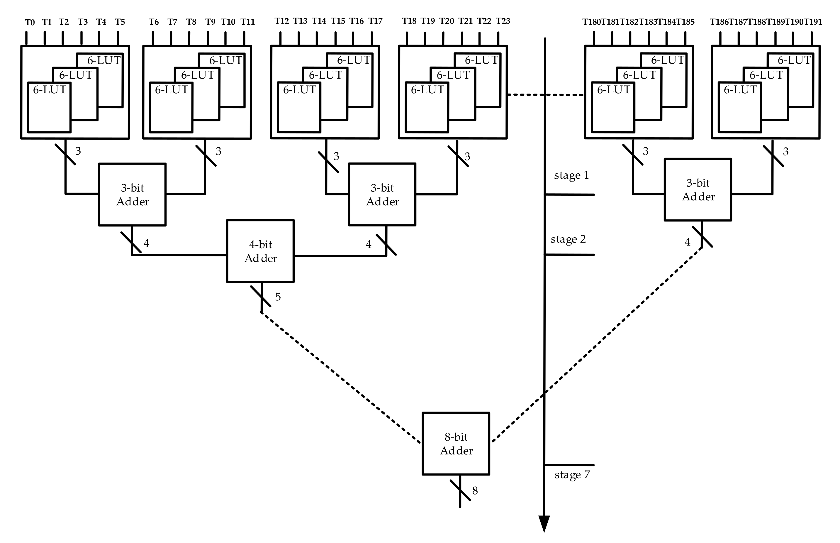
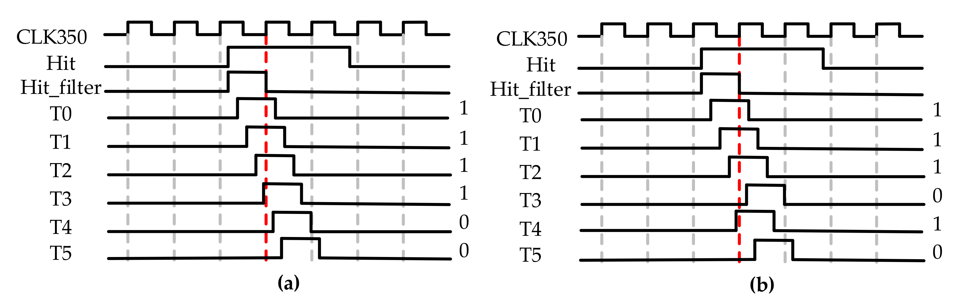
2.2. One-Counter Encoder
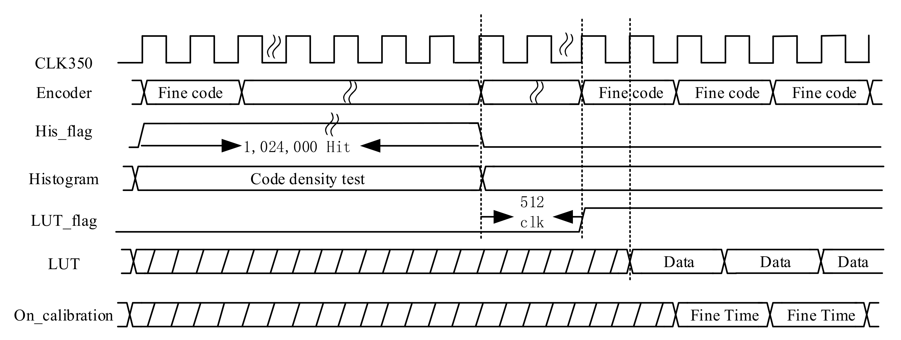
2.3. Online Calibration
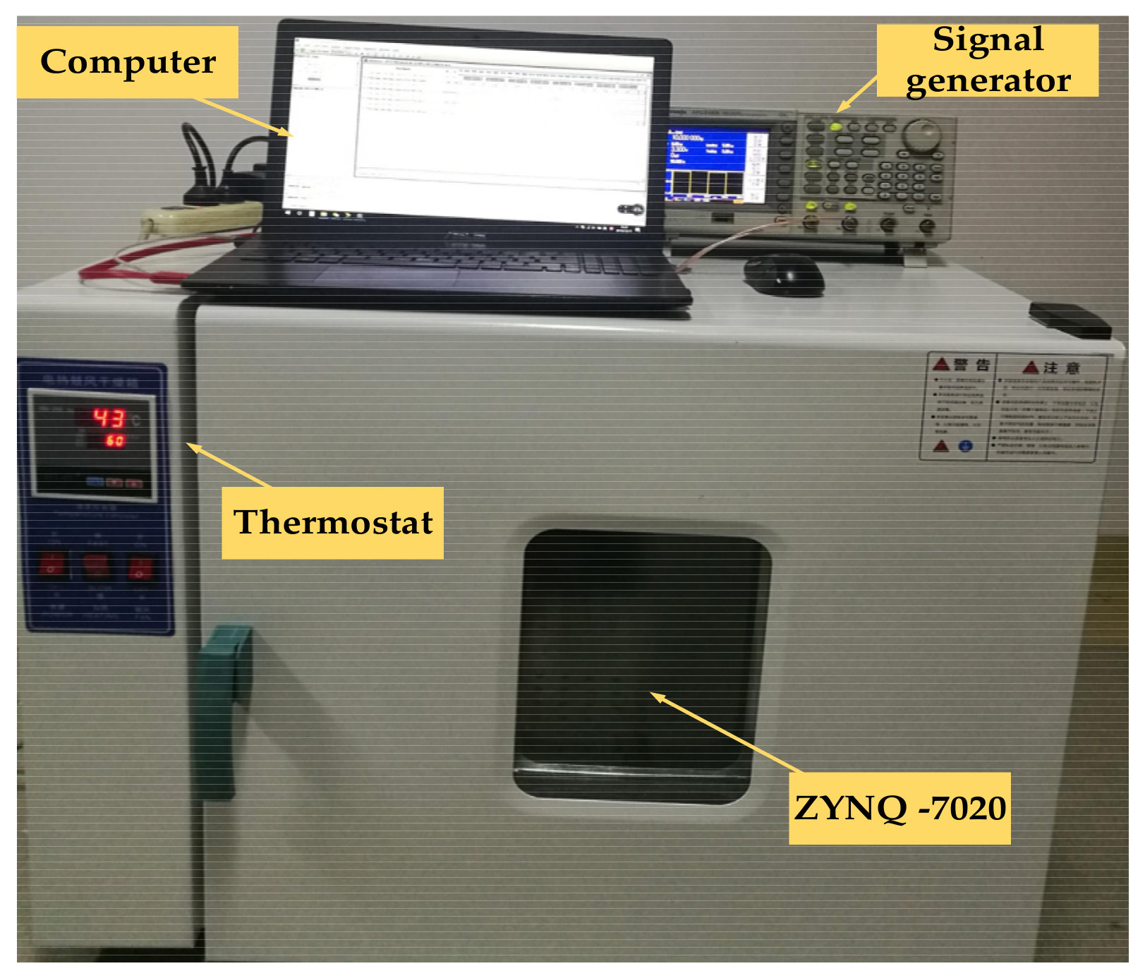
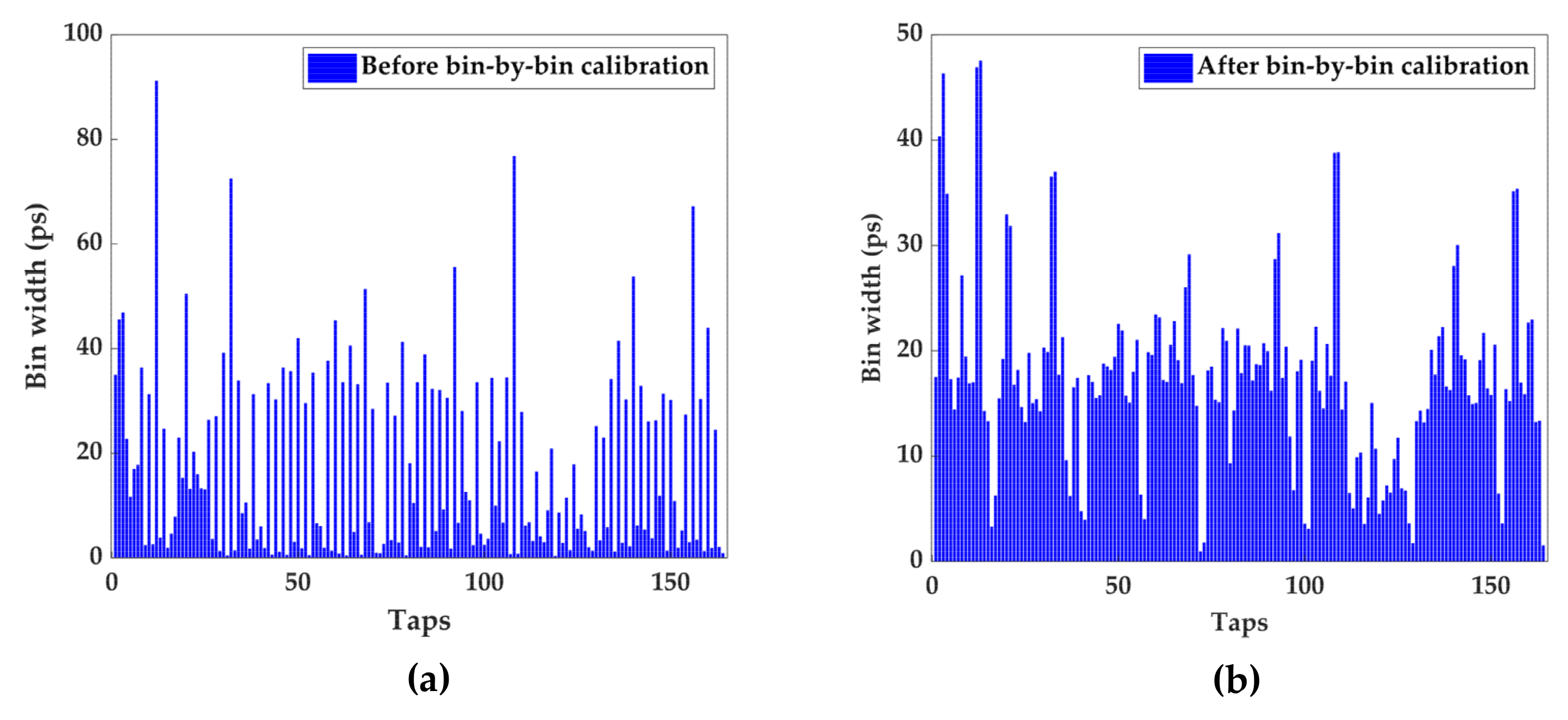
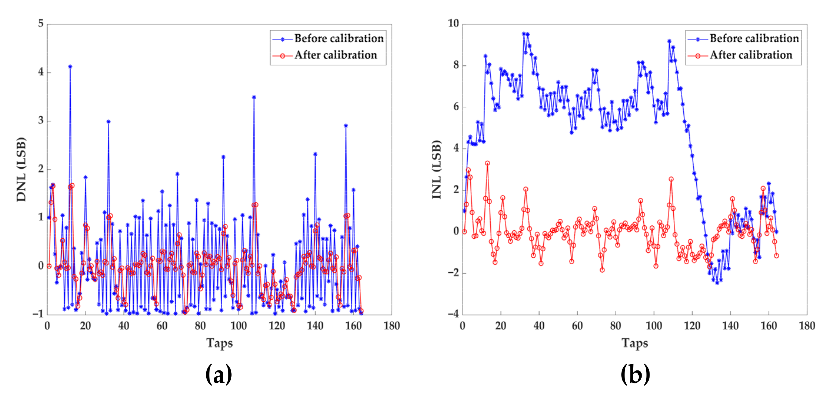
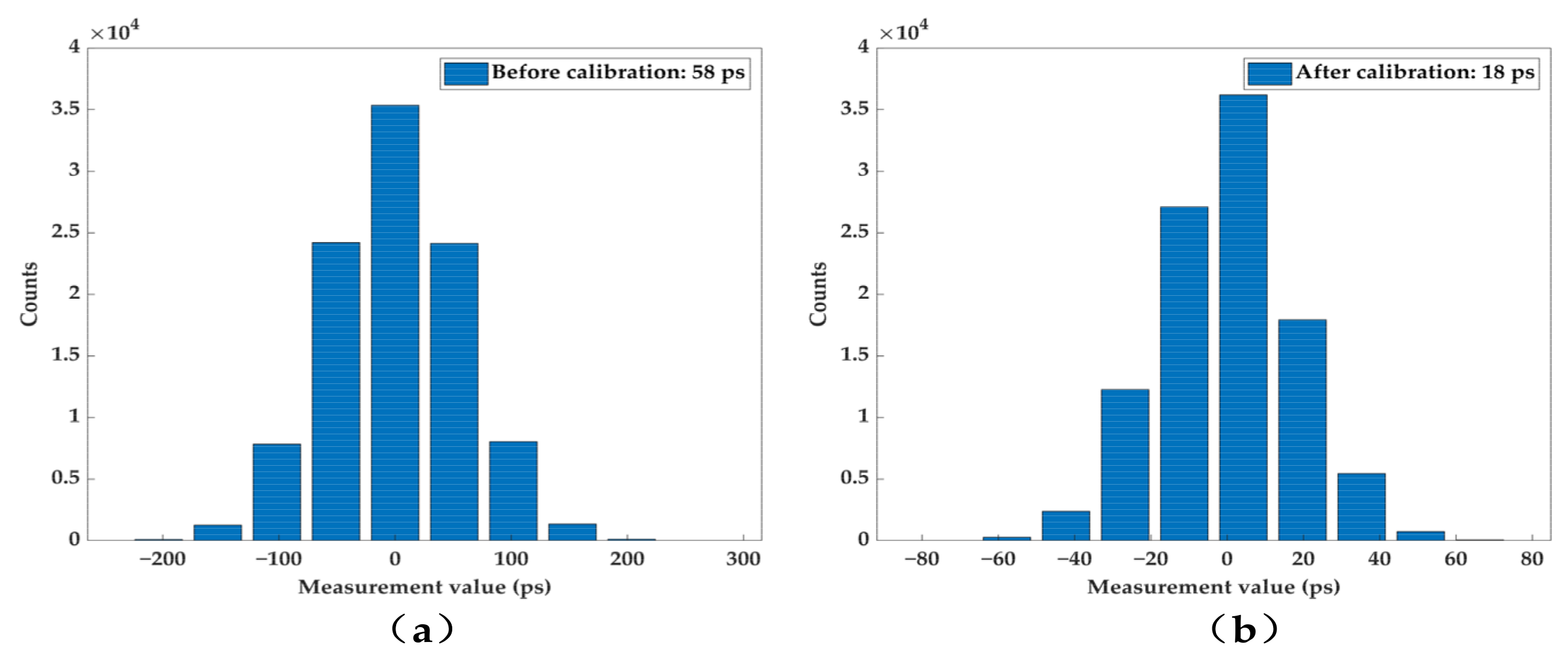
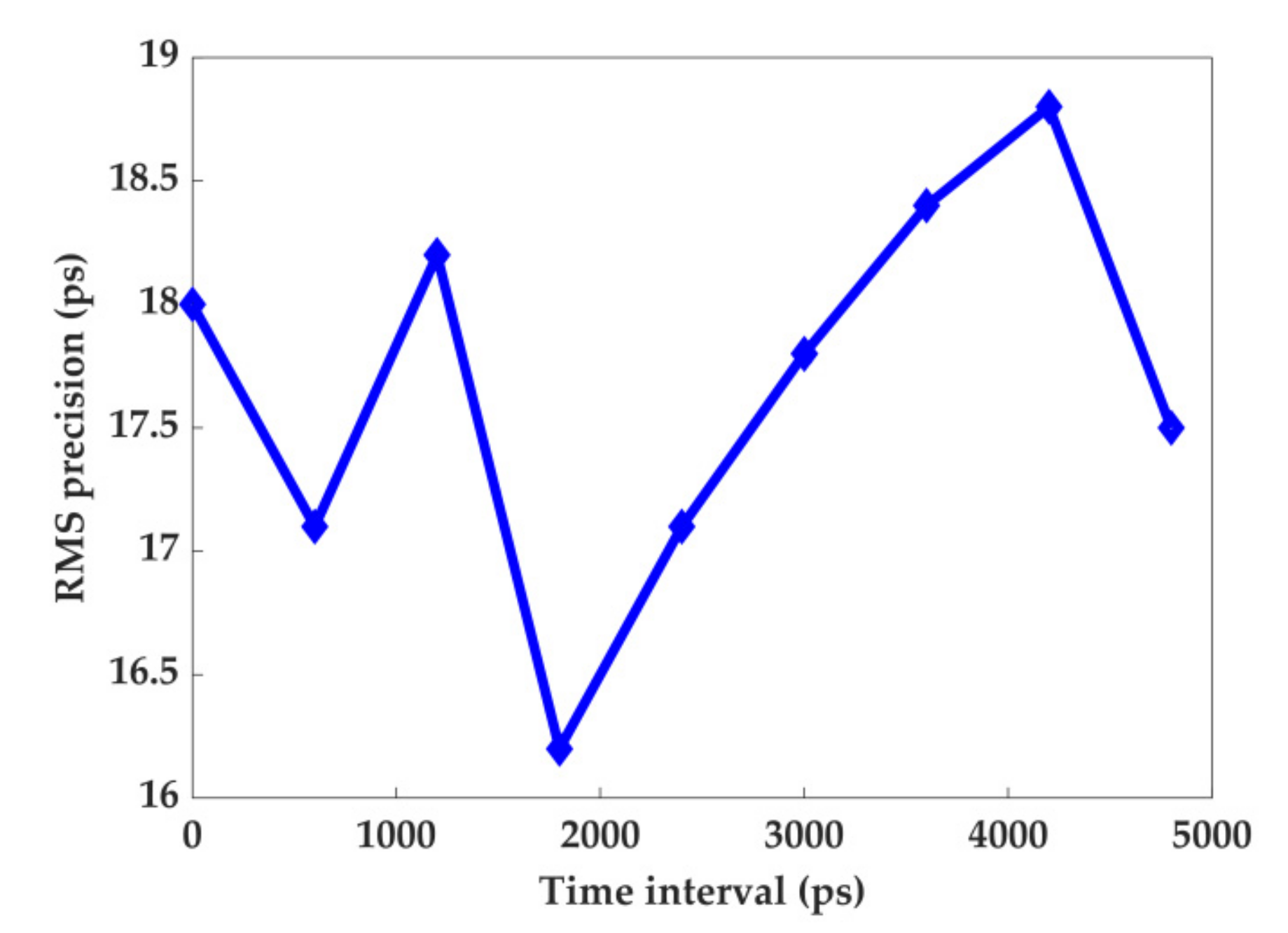
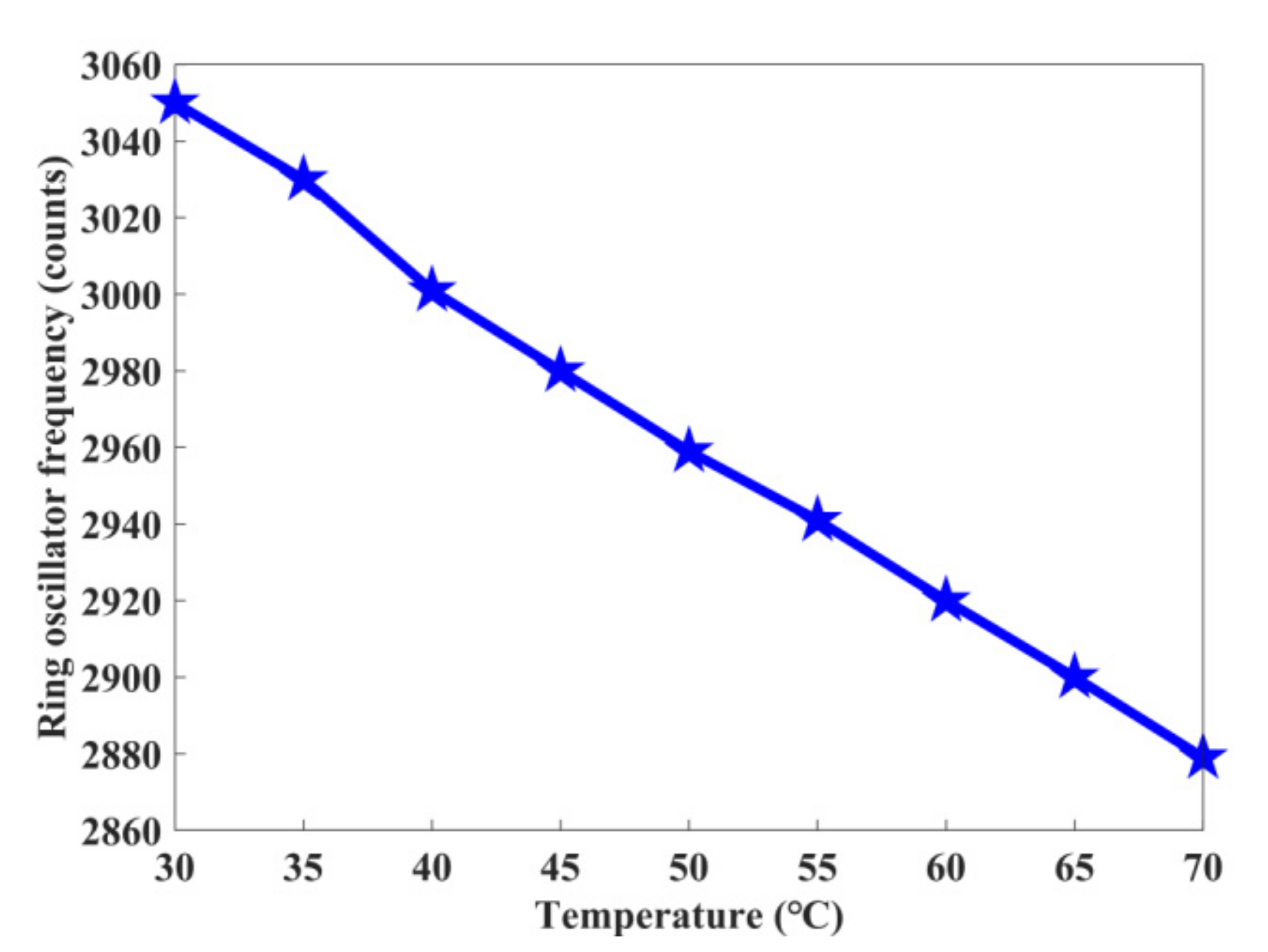
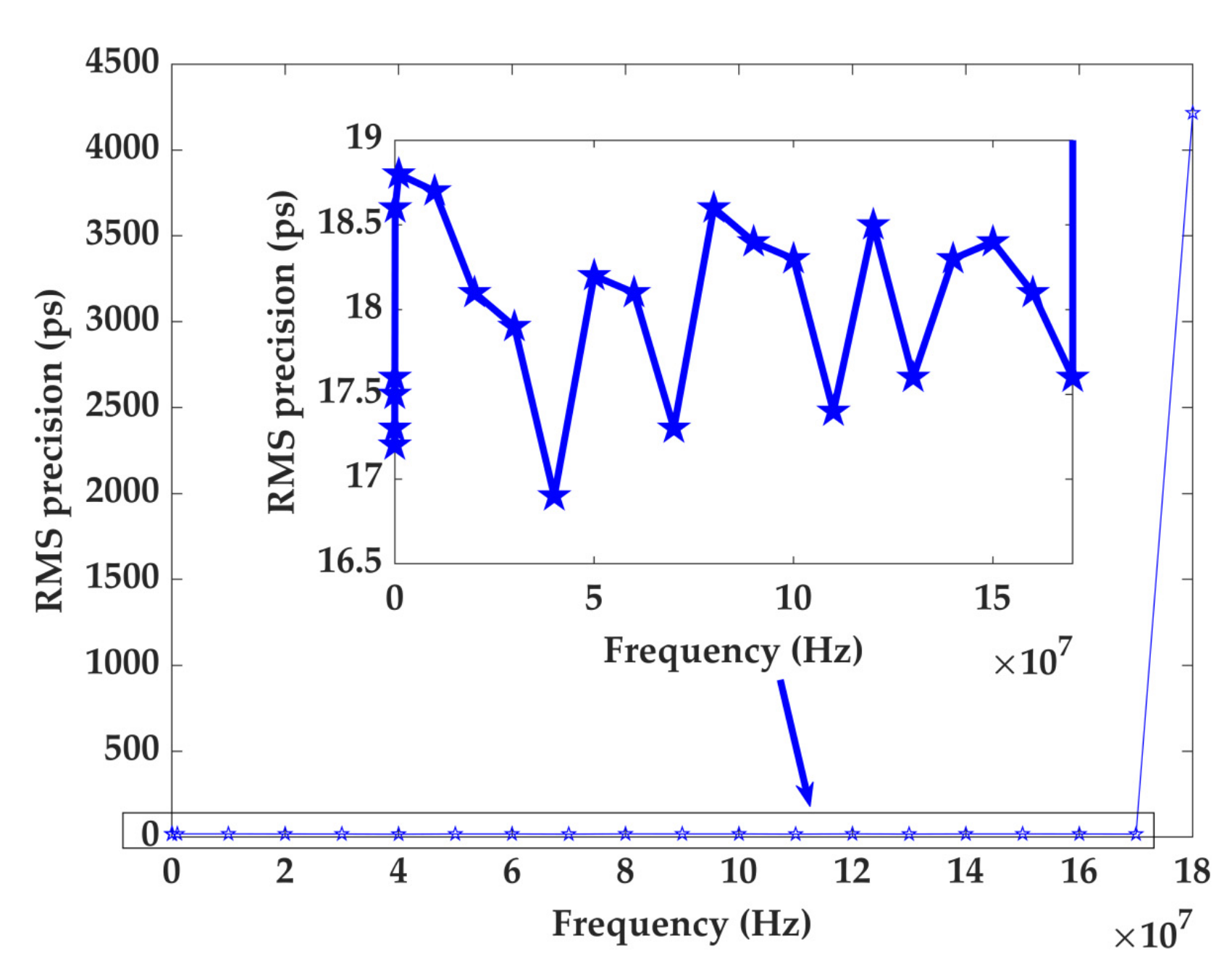
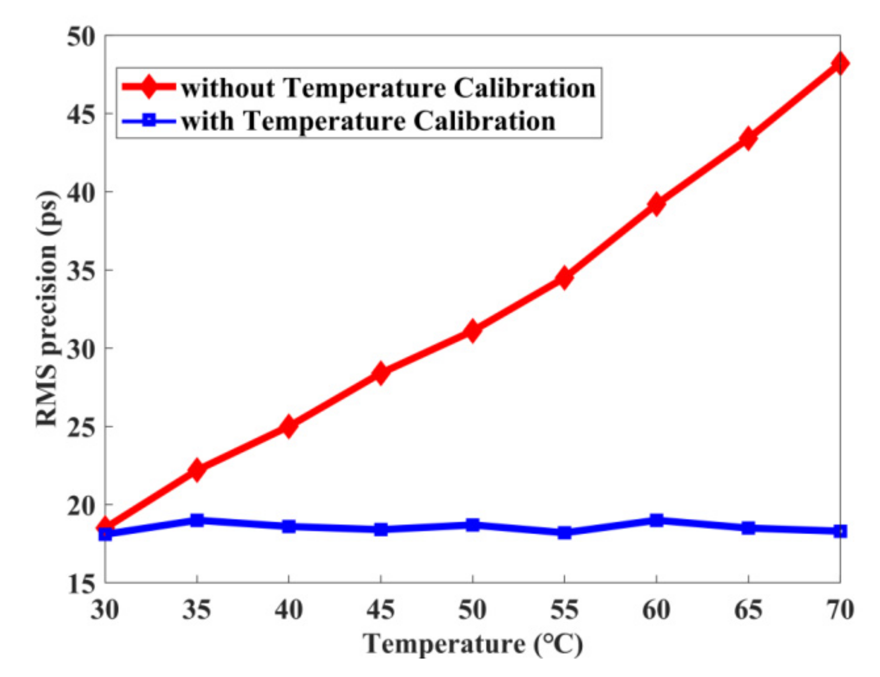
3. Results
4. Conclusions
Author Contributions
Funding
Institutional Review Board Statement
Informed Consent Statement
Data Availability Statement
Conflicts of Interest
References
- Russo, S.; Petra, N.; De Caro, D.; Barbarino, G.; Strollo, A.G. A 41 ps ASIC time-to-digital converter for physics experiments. Nucl. Instrum. Methods Phys. Res. Sect. A Accel. Spectrom. Detect. Assoc. Equip. 2011, 659, 422–427. [Google Scholar] [CrossRef]
- Tang, Y.; Townsend, T.; Deng, H.; Liu, Y.; Zhang, R.; Chen, J. A Highly Linear FPGA-Based TDC and a Low-Power Multichannel Readout ASIC With a Shared SAR ADC for SiPM Detectors. IEEE Trans. Nucl. Sci. 2021, 68, 2286–2293. [Google Scholar] [CrossRef]
- Kuang, J.; Wang, Y.; Cao, Q.; Liu, C. Implementation of a high precision multi-measurement time-to-digital convertor on a Kintex-7 FPGA. Nucl. Instrum. Methods Phys. Res. Sect. A Accel. Spectrom. Detect. Assoc. Equip. 2018, 891, 37–41. [Google Scholar] [CrossRef]
- Hong, K.J.; Kim, E.; Yeom, J.Y.; Olcott, P.D.; Levin, C.S. FPGA-based time-to-digital converter for time-of-flight PET detector. In Proceedings of the 2012 IEEE Nuclear Science Symposium and Medical Imaging Conference Record (NSS/MIC), Anaheim, CA, USA, 27 October–3 November 2012; pp. 2463–2465. [Google Scholar]
- Vornicu, I.; Carmona-Galán, R.; Rodríguez-Vázquez, Á. Arrayable voltage-controlled ring-oscillator for direct time-of-flight image sensors. IEEE Trans. Circuits Syst. I Regul. Pap. 2017, 64, 2821–2834. [Google Scholar] [CrossRef]
- Marino, N.; Baronti, F.; Fanucci, L.; Saponara, S.; Roncella, R.; Bisogni, M.G.; Del Guerra, A. A multichannel and compact time to digital converter for time of flight positron emission tomography. IEEE Trans. Nucl. Sci. 2015, 62, 814–823. [Google Scholar] [CrossRef]
- Moses, W.; Buckley, S.; Vu, C.; Peng, Q.; Pavlov, N.; Choong, W.-S.; Wu, J.; Jackson, C. OpenPET: A flexible electronics system for radiotracer imaging. IEEE Trans. Nucl. Sci. 2010, 57, 2532–2537. [Google Scholar] [CrossRef] [Green Version]
- Hervé, C.; Cerrai, J.; Le Caër, T. High resolution time-to-digital converter (TDC) implemented in field programmable gate array (FPGA) with compensated process voltage and temperature (PVT) variations. Nucl. Instrum. Methods Phys. Res. Sect. A Accel. Spectrom. Detect. Assoc. Equip. 2012, 682, 16–25. [Google Scholar] [CrossRef]
- Garzetti, F.; Corna, N.; Lusardi, N.; Geraci, A. Time-to-Digital Converter IP-Core for FPGA at State of the Art. IEEE Access 2021, 9, 85515–85528. [Google Scholar] [CrossRef]
- Cui, K.; Li, X. A high-linearity Vernier time-to-digital converter on FPGAs with improved resolution using bidirectional-operating Vernier delay lines. IEEE Trans. Instrum. Meas. 2019, 69, 5941–5949. [Google Scholar] [CrossRef]
- Cui, K.; Ren, Z.; Li, X.; Liu, Z.; Zhu, R. A high-linearity, ring-oscillator-based, Vernier time-to-digital converter utilizing carry chains in FPGAs. IEEE Trans. Nucl. Sci. 2016, 64, 697–704. [Google Scholar] [CrossRef]
- Balla, A.; Beretta, M.M.; Ciambrone, P.; Gatta, M.; Gonnella, F.; Iafolla, L.; Mascolo, M.; Messi, R.; Moricciani, D.; Riondino, D. The characterization and application of a low resource FPGA-based time to digital converter. Nucl. Instrum. Methods Phys. Res. Sect. A Accel. Spectrom. Detect. Assoc. Equip. 2014, 739, 75–82. [Google Scholar] [CrossRef]
- Büchele, M.; Fischer, H.; Gorzellik, M.; Herrmann, F.; Königsmann, K.; Schill, C.; Schopferer, S. A 128-channel Time-to-Digital Converter (TDC) inside a Virtex-5 FPGA on the GANDALF module. J. Instrum. 2012, 7, C03008. [Google Scholar] [CrossRef]
- Chen, H.; Zhang, Y.; Li, D.D.-U. A low nonlinearity, missing-code free time-to-digital converter based on 28-nm FPGAs with embedded bin-width calibrations. IEEE Trans. Instrum. Meas. 2017, 66, 1912–1921. [Google Scholar] [CrossRef] [Green Version]
- Won, J.Y.; Lee, J.S. Time-to-Digital Converter Using a Tuned-Delay Line Evaluated in 28-, 40-, and 45-nm FPGAs. IEEE Trans. Instrum. Meas. 2016, 65, 1678–1689. [Google Scholar] [CrossRef]
- Wang, Y.; Xie, W.; Chen, H.; Li, D.D.U. Multichannel time-to-digital converters with automatic calibration in Xilinx Zynq-7000 FPGA devices. IEEE Trans. Ind. Electron. 2021. [Google Scholar] [CrossRef]
- Wang, Y.; Kuang, P.; Liu, C. A 256-channel multi-phase clock sampling-based time-to-digital converter implemented in a Kintex-7 FPGA. In Proceedings of the 2016 IEEE International Instrumentation and Measurement Technology Conference Proceedings, Taipei, Taiwan, 23–26 May 2016; pp. 1–5. [Google Scholar]
- Wu, J. Several Key Issues on Implementing Delay Line Based TDCs Using FPGAs. IEEE Trans. Nucl. Sci. 2010, 57, 1543–1548. [Google Scholar] [CrossRef]
- Fishburn, M.; Menninga, L.H.; Favi, C.; Charbon, E. A 19.6 ps, FPGA-Based TDC With Multiple Channels for Open Source Applications. IEEE Trans. Nucl. Sci. 2013, 60, 2203–2208. [Google Scholar] [CrossRef]
- Wang, Y.; Kuang, J.; Liu, C.; Cao, Q. A 3.9-ps RMS Precision Time-to-Digital Converter Using Ones-Counter Encoding Scheme in a Kintex-7 FPGA. IEEE Trans. Nucl. Sci. 2017, 64, 2713–2718. [Google Scholar] [CrossRef]
- Wang, J.; Liu, S.; Shen, Q.; Li, H.; An, Q. A fully fledged TDC implemented in field-programmable gate arrays. IEEE Trans. Nucl. Sci. 2010, 57, 446–450. [Google Scholar] [CrossRef]
- Tontini, A.; Gasparini, L.; Pancheri, L.; Passerone, R. Design and characterization of a low-cost FPGA-based TDC. IEEE Trans. Nucl. Sci. 2018, 65, 680–690. [Google Scholar] [CrossRef]
- Chen, Y.-H. Time resolution improvement using dual delay lines for field-programmable-gate-array-based time-to-digital converters with real-time calibration. Appl. Sci. 2019, 9, 20. [Google Scholar] [CrossRef] [Green Version]
- Lusardi, N.; Garzetti, F.; Corna, N.; Marco, R.D.; Geraci, A. Very High-Performance 24-Channels Time-to-Digital Converter in Xilinx 20-nm Kintex UltraScale FPGA. In Proceedings of the 2019 IEEE Nuclear Science Symposium and Medical Imaging Conference (NSS/MIC), Manchester, UK, 26 October–2 November 2019; pp. 1–4. [Google Scholar]
- Parsakordasiabi, M.; Vornicu, I.; Rodríguez-Vázquez, Á.; Carmona-Galán, R. A Low-Resources TDC for Multi-Channel Direct ToF Readout Based on a 28-nm FPGA. Sensors 2021, 21, 308. [Google Scholar] [CrossRef] [PubMed]
- Lusardi, N.; Garzetti, F.; Corna, N.; Salgaro, S.; Bachetti, N.; Geraci, A. Plug-and-Play Tunable and High-Performance Time-to-Digital Converter as IP-Core for Xilinx FPGAs. In Proceedings of the 2020 IEEE Nuclear Science Symposium and Medical Imaging Conference (NSS/MIC), Boston, MA, USA, 31 October–7 November 2020; pp. 1–3. [Google Scholar]
- Chen, Z.; Shi, W.; Xiong, G.; Yang, J.; Xu, Y. A 63.3 ps TDC Measurement System Based on FPGA for Pulsed Laser Ranging. In Proceedings of the 2019 IEEE 13th International Conference on ASIC (ASICON), Chongqing, China, 29 October–1 November 2019; pp. 1–4. [Google Scholar]
- Sail, E.; Vesterbacka, M. A multiplexer based decoder for flash analog-to-digital converters. In Proceedings of the 2004 IEEE Region 10 Conference TENCON 2004, Chiang Mai, Thailand, 24 November 2004; Volume 254, pp. 250–253. [Google Scholar]
- Zheng, J.; Cao, P.; Jiang, D.; An, Q. Low-Cost FPGA TDC With High Resolution and Density. IEEE Trans. Nucl. Sci. 2017, 64, 1401–1408. [Google Scholar] [CrossRef]
- Cao, G.; Xia, H.; Dong, N. An 18-ps TDC using timing adjustment and bin realignment methods in a Cyclone-IV FPGA. Rev. Sci. Instrum. 2018, 89, 054707. [Google Scholar] [CrossRef]
- Wu, J.; Shi, Z. The 10-ps wave union TDC: Improving FPGA TDC resolution beyond its cell delay. In Proceedings of the 2008 IEEE Nuclear Science Symposium Conference Record, Dresden, Germany, 19–25 October 2008; pp. 3440–3446. [Google Scholar]


| Abbreviations | Description |
|---|---|
| TDC | Time-to-digital converter |
| FPGA | Field Programmable Gate Array |
| CARRY4 | Slice primitive: Fast Carry Logic with Look Ahead |
| LSB | least significant bit |
| PET | positron emission tomograph |
| ASIC | Application Specific Integrated Circuit |
| VDL | Vernier delay line |
| MCP | multiple clock phases |
| TDL | tapped delay line |
| STA | static timing analysis |
| DNL | differential nonlinearities |
| INL | integral nonlinearities |
| MMCM | mixed-mode clock manager |
| LDO | low dropout regulator |
| IDELAYCTRL | Xilinx primitive: IDELAYE2/ODELAYE2 Tap Delay Value Control |
| IDELAYE2 | Xilinx primitive: Input Fixed or Variable Delay Element |
| Hex Numbers | Binary Numbers |
|---|---|
| 6996966996696996 | 01101001100101101001011001101001 10010110011010010110100110010110 |
| 8117177E177E7EE8 | 10000001000101110001011101111110 00010111011111100111111011101000 |
| FEE8E880E8808000 | 11111110111010001110100010000000 11101000100000001000000000000000 |
| Component | Worst Negative Slack |
|---|---|
| Setup | 0.348 ns |
| Hold | 0.068 ns |
| Module | LUTs (53200) | FFs (106400) | BRAMs (140) |
|---|---|---|---|
| TDC core | 522 | 1080 | 4 |
| One channel TDC system | 1551 | 2313 | 4 |
| Two channel TDC system | 2513 | 4095 | 8 |
| Component | Power |
|---|---|
| Total dynamic | 1.601 W |
| Clocks dynamic | 1.399 W |
| Logic dynamic | 0.015 W |
| BRAM dynamic | 0.014 W |
| MMCM dynamic | 0.123 W |
| PS | 1.399 W |
| Total static | 0.138 W |
| Ref | Used Method | FPGA | LSB [ps] | Precision [ps] | DNL [LSB] | INL [LSB] | Sample Rate [Ms/s] | Resources | Power |
|---|---|---|---|---|---|---|---|---|---|
| 2018 [30] | TDL | Cyclone-IV | 45 | 18 | [−0.5, 0.13] | [−0.48, 0.37] | 75 | - | - |
| 2018 [3] | TDL | Kintex-7 | 3 | 5.76 | - | [−9, 9] | 45.5 | - | - |
| 2018 [22] | TDL | Spartan-6 | 25.6 | 37 | [−0.90, 1.23] | [−0.0.43, 2.96] | 115 | 415 Slices | 0.131 W |
| 2021 [25] | TDL | Artix-7 | 22.2 | 26.04 | [−0.95, 1.19] | [−2.75, 1.24] | 125 | 216 LUTs | 0.164 W |
| This work | TDL | ZYNQ-7020 | 17.4 | 19 | [−0.90, 1.67] | [−1.90, 3.31] | 170 | 522 LUTs | 0.340 W |
Publisher’s Note: MDPI stays neutral with regard to jurisdictional claims in published maps and institutional affiliations. |
© 2022 by the authors. Licensee MDPI, Basel, Switzerland. This article is an open access article distributed under the terms and conditions of the Creative Commons Attribution (CC BY) license (https://creativecommons.org/licenses/by/4.0/).
Share and Cite
Zhang, M.; Zhao, Y.; Han, Z.; Zhao, F. A 19 ps Precision and 170 M Samples/s Time-to-Digital Converter Implemented in FPGA with Online Calibration. Appl. Sci. 2022, 12, 3649. https://doi.org/10.3390/app12073649
Zhang M, Zhao Y, Han Z, Zhao F. A 19 ps Precision and 170 M Samples/s Time-to-Digital Converter Implemented in FPGA with Online Calibration. Applied Sciences. 2022; 12(7):3649. https://doi.org/10.3390/app12073649
Chicago/Turabian StyleZhang, Mengdi, Ye Zhao, Zhengsheng Han, and Fazhan Zhao. 2022. "A 19 ps Precision and 170 M Samples/s Time-to-Digital Converter Implemented in FPGA with Online Calibration" Applied Sciences 12, no. 7: 3649. https://doi.org/10.3390/app12073649
APA StyleZhang, M., Zhao, Y., Han, Z., & Zhao, F. (2022). A 19 ps Precision and 170 M Samples/s Time-to-Digital Converter Implemented in FPGA with Online Calibration. Applied Sciences, 12(7), 3649. https://doi.org/10.3390/app12073649