1. Introduction
Crystalline silicon nanowires (SiNWs) usually exhibit a highly efficient light absorption and an antireflection of the incident light greater than that of a flat surface silicon material of the same size [
1]. Geometrical scattering and antenna effect of the SiNWs are the main reasons for high light-harvesting performance [
2,
3], where the NW density and diameter determine the absorbed wavelength, which is called the resonance wavelength [
4]. One more advantage of the SiNW solar cell is the simplicity of the fabrication process with a large-area scalable structure, as introduced by Garnett and Yang [
5]. This process produced a high open-circuit voltage value,
Voc, and high fill factor,
FF, which lead to producing higher overall efficiency,
µ, of the solar cell for high values of short-circuit current density,
Jsc. However, we still need to increase the value of the
Jsc, which can be obtained by using an absorber layer, such as graphene,
C [
6]. For its good electric properties, as a thin and highly transparent material, graphene has been greatly used in recent research [
7]. Graphene on a silicon surface forms a Schottky junction solar cell with a very low efficiency, which can be improved by engineering the interface with a passivation layer to increase the graphene work function [
8]. On the other hand, plasmonic nanoparticles have high absorption properties which depend on the surrounding medium and the size, shape, and material of the nanoparticles [
9]. In this work, we used a graphene layer and plasmonic NPs distributed on the top of a silicon surface to enhance the power conversion efficiency (PCE) of the SiNW solar cell [
10,
11,
12].
Large-area SiNWs with radial PN junctions have been produced using a simple fabrication method by Garnett and Yang [
5]. The fabricated solar cell was based on a room-temperature aqueous etching method and low-temperature thin film deposition with a rapid thermal annealing crystallization process. The given method increased the PCE to be 5.3% with
Voc = 0.56 V,
FF = 0.607, and
Jsc = 17.32 mA/cm
2.
A SiNW solar cell grown on a silicon base and covered with an on-site graphene layer for Schottky junction was introduced by Wallace et al. [
6]. The graphene layer increased the carrier collection and enhanced the solar cell efficiency to be 3.83%. The obtained open-circuit voltage is 0.47 V, the fill factor is 0.59, and the short-circuit current density is 13.7 mA/cm
2. Linwei Yu and Pere Cabarrocas fabricated a SiNW nanostructure on a silicon base photovoltaic, which achieved light absorption [
1]. In addition, a 3D radial junction solar cell has been developed in order to overcome light-induced degradation. The experimental results illustrated that the maximum obtained open-circuit voltage from the solar cell is 0.82 V and the
FF is 0.73, while the short-circuit current density is 15.2 mA/cm
2, which leads to a power conversion efficiency of 9.3%. A large-scale silicon solar microcell fabricated from bulk wafers using transferring printing technique was presented by Yoon et al. [
13]. The produced device has many features such as mechanical flexibility, transparency, and ultrathin microconcentrator designs. Theoretical and experimental electrical, mechanical, and optical characteristics of several types of modules were illustrated in this work. The measured
Voc is 0.51,
FF is 0.61,
Jsc is 33.6 mA/cm
2, and PCE is 11.6%.
Augusto et al. showed the analytical model of the recombination mechanisms of a silicon solar cell with low bandgap-voltage offset [
14]. The work showed the effect of changing excess carrier density on the effective lifetime of the carriers. The untextured structure, with 50 µm thickness, produced 0.764 V as an open-circuit voltage, a fill factor of 0.86, and a short-circuit current density of 38.8 mA/cm
2.
Moreover, the surface plasmon localization (SPL) technique on plasmonic nanoparticles is used as an efficient method to improve the optical absorption of solar cells, metal–dielectric–metal, and metamaterial applications [
15,
16,
17,
18,
19]. The NP shapes and materials are the main parameters that affect the solar cell and sensor performance [
20,
21,
22,
23].
In this paper, the light harvesting of SiNW solar cells has been improved by using a graphene layer and gold nanoparticles. Short-circuit current density, power conversion efficiency, and light absorption are simulated by applying a finite difference time domain method using the Lumerical FDTD solutions software package. The effect of changing excess carrier concentration on the PCE is also illustrated in this work. For different nanoparticle materials, the light absorption and PCE are illustrated as a function of the wavelengths. Moreover, the effects of NW length and separation between two successive NWs are also given in this work. In addition, the optical power distribution in different monitoring layers for different proposed solar cell structures is given in this work.
2. Analytical Model
The overall solar cell efficiency can be calculated using a single diode model and by applying the Green empirical expression [
4]. Short-circuit current density,
Jsc, can be calculated using Equation (1) by assuming that an incident photon will produce an electron [
9].
where
q is the electron charge,
h is the Planck constant,
c is the speed of light,
I(λ) is the standard air mass 1.5 (AM1.5) spectral irradiance, and
A(λ) is the optical absorption. On the other hand, the open-circuit voltage,
Voc, of silicon nanowire pillars is given by Equation (2) [
24].
where
is the thermal voltage which equals 25.8 mV,
NA is the doping concentration (
NA = 3.3 × 10
17 cm
−3),
is the excess carrier concentration for
n-type (
) [
11], and
ni is the intrinsic carrier concentration. The open-circuit voltage of the silicon nanowires can be calculated and considered as a fixed value equal to 0.626 V as it depends on the energy level of the material and for
at room temperature.
Hence, the fill factor can be calculated using Equation (3) [
9].
The maximum output power,
Pmax, can be calculated using Equation (4).
Hence, the overall solar cell efficiency, η, can be calculated as a ratio of maximum output power to solar input power.
Gold,
Au, plasmonic nanoparticles distributed on the substrate layer will change the optical power absorbed in the active layer and depend on the maximum value of reflectivity. Nanoparticle shape has a great effect on the transmitted optical power as well as the relative permittivity of the gold nanoparticles and the dielectric function of the surrounding medium [
9]. The maximum reflectivity can be calculated using Equation (5).
where
εm is the permittivity of the surrounding medium,
εAu is a gold nanoparticle dielectric constant at corresponding
λmax,
g is an integer, and
L is structural periodicity. Hence, the dielectric permittivity can be expressed by using a multioscillator Drude–Lorentz model [
9] as given in Equation (6):
where
εꝏ is the gold high-frequency dielectric permittivity,
ωD and
γD are the plasma and collision frequencies of the free electron gas,
δk is the amplitude of Lorentz oscillator,
ωk is the resonance angular frequencies, and
γk is the damping constants for k value from 1 to 6.
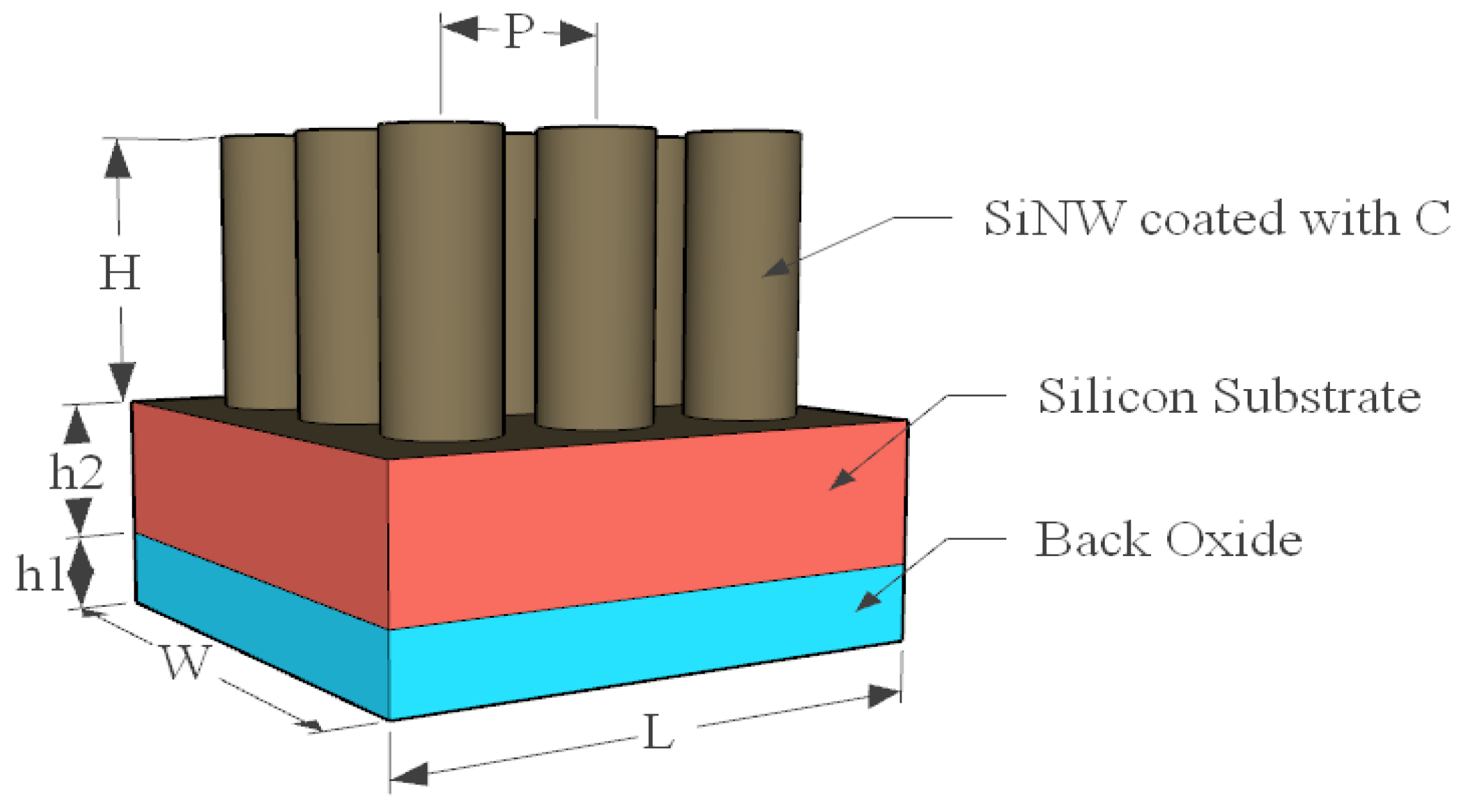
3. Proposed Structure
In this work, we used an electromagnetic wave solver, Lumerical FDTD solutions software, to design and analyze the proposed structure. A unit cell of the proposed structure has been simulated using the FDTD method. The overall dimensions of the unit cell are 500 × 500 × 700 nm
3 in the three dimensions
x,
y, and
z, respectively. A silicon substrate with height
h2 = 3 µm is placed on the top of a back oxide material with height
h1 = 1 µm, as illustrated in
Figure 1. Silicon nanowires are grown on the top of the silicon substrate with height
H = 5 µm and period
P = 550 nm between each NW. In addition to that, a graphene layer can be used on the top of substrate material and on the NWs as well.
The boundary conditions are considered as periodic structures in x-direction and y-direction, as the structure is extended in both x- and y-dimensions, and perfect matching layer in z-direction, as the structure is not repeated in z-direction, where the minimum mesh size is 20 nm in all directions. A plane wave source with wavelength band 400–1100 nm and offset time 7.5 fs is used as a light source. In addition, the solar generation calculation region is given in the active layer to calculate the short-circuit current density.
The refractive index of back oxide is 1.4; however, the value for silicon is a function of the wavelength and follows the Aspnes and Studna model [
25], and the refractive index of graphene follows the Phillip and Taft model [
26]. On the other hand, the refractive index of plasmonic NPs is summarized using Equation (6) in
Table 1 [
27].
4. Results and Discussion
To maximize the absorbed light in the visible and NIR regions, which leads to an increase in the
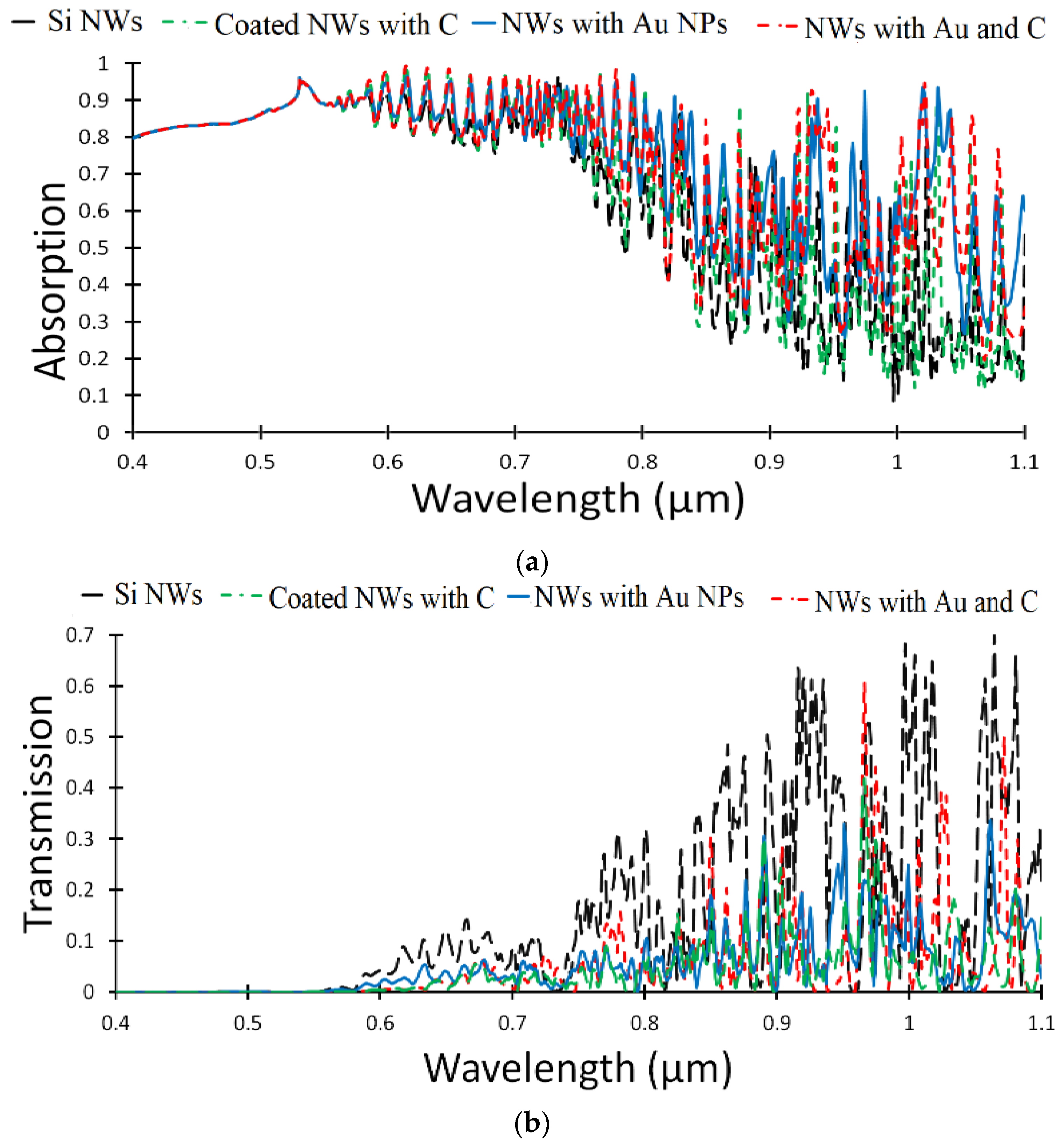
Jsc and the overall frequency, different proposals will be produced. The absorption of a traditional SiNW solar cell will be compared to SiNWs coated with a 2D graphene layer and with/without Au plasmonic nanoparticles distributed on the silicon substrate layer.
Figure 2a,b illustrates the absorption and transmission of the four proposed techniques. As shown in
Figure 2a, the absorptions of the traditional SiNWs and of SiNWs coated with graphene are almost the same; however, a high absorption has been obtained when Au NPs are distributed on the top silicon substrate surface. The light transmitted through the solar cell is illustrated given in
Figure 2b. However, it is very hard to distinguish between four cases, so the short-circuit current density and consequently PCE is the used in such case to choose which structure has better performance.
The resultant short-circuit current density and the power conversion efficiency for each structure are given in
Table 2. The maximum
Jsc, 34.72 mA/cm
2, is obtained when the SiNWs coated with a graphene layer and Au NPs are distributed on the silicon substrate surface, which gives maximum overall efficiency, 15.8%, as shown in
Table 2.
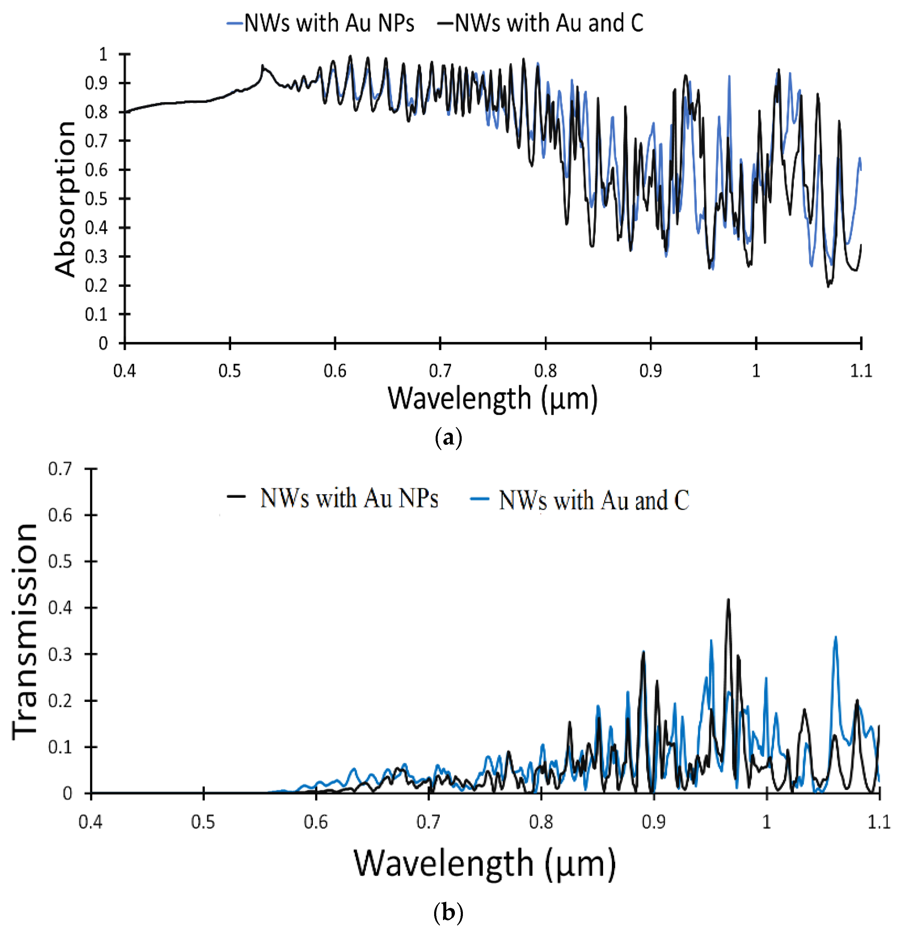
The absorbed light is increased and the short-circuit current density and power conversion efficiency are consequently increased as the graphene layer is added, due to its high absorption properties. On the other hand, adding Au NPs increased the absorbed light according to Equations (5) and (6). To compare between the given two structures, SiNWs with Au NPs and with/without graphene layer, the absorption and transmission are illustrated in
Figure 3a,b.
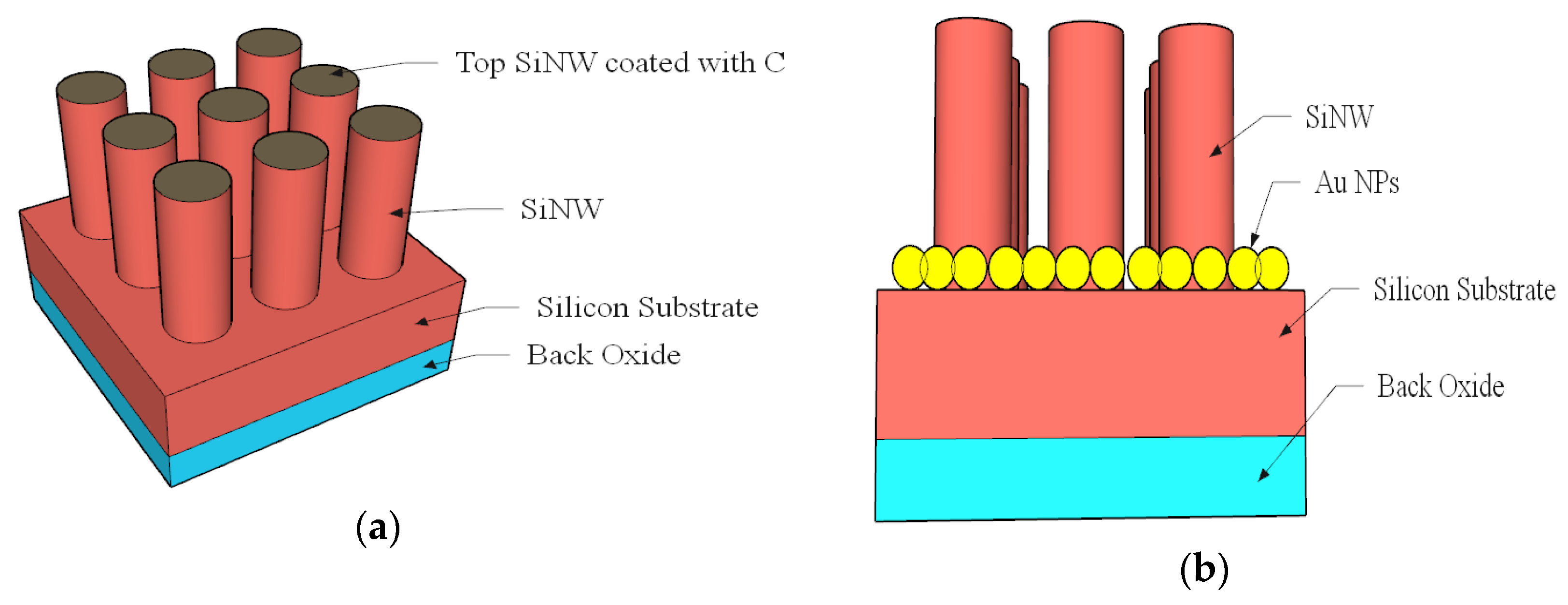
To increase the efficiency of the solar cell, Au NPs are distributed on the top silicon surface directly, without using the graphene layer, and the graphene layer is used to coat the top surface of the SiNWs, as illustrated in
Figure 4a,b. The obtained short-circuit current density is 41.7 mA/cm
2 and the overall solar cell efficiency is 19.0%. A 3D structure of the configuration using the graphene layer is shown in
Figure 4a, and the side view of the structure is given in
Figure 4b. The graphene layer, on the top of NWs, absorbs the incident light and retransmits it into the NWs, which behave as nanoantennas, while the plasmonic Au NPs absorb the light and transfer it to the silicon substrate.
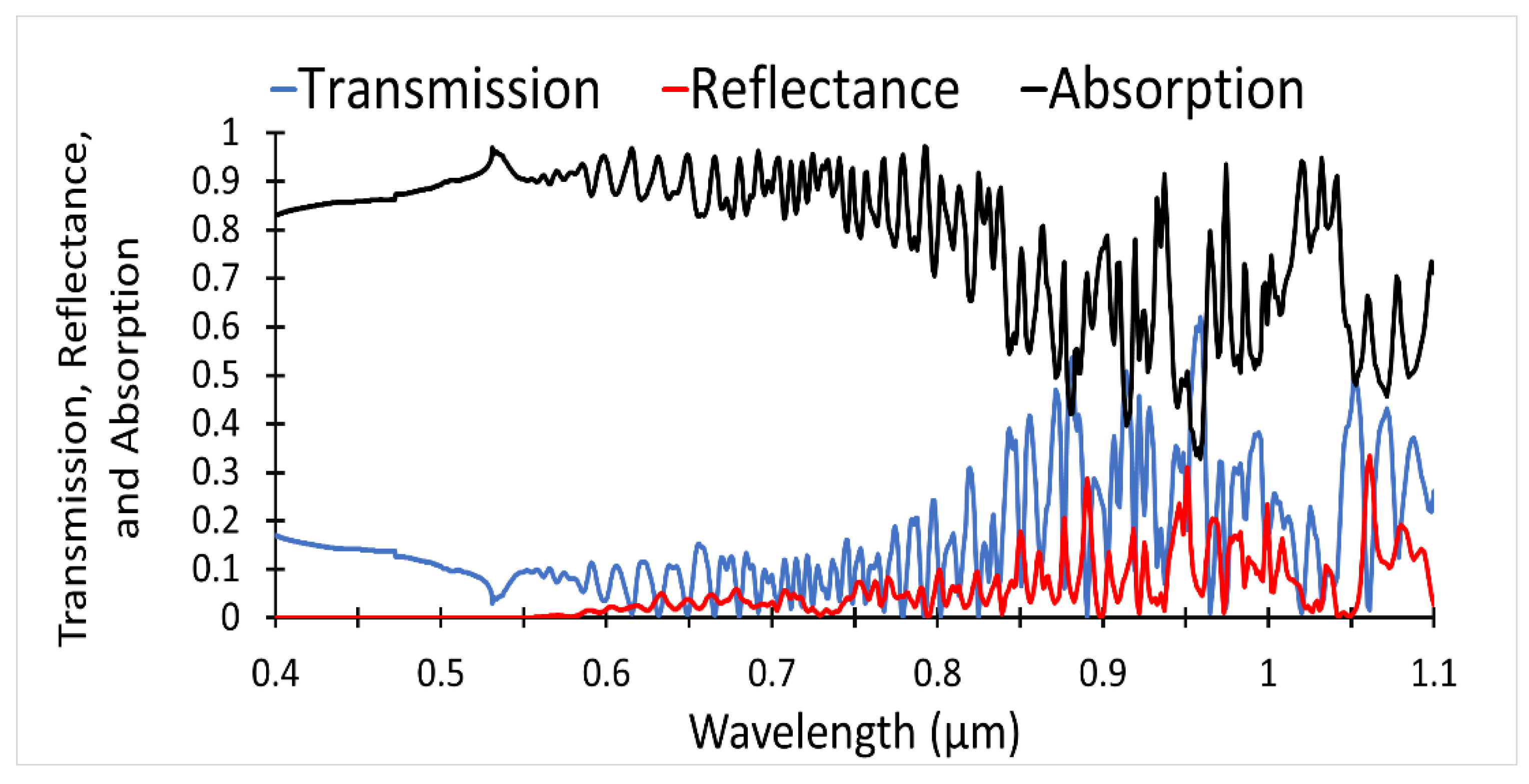
Figure 5 shows the absorption, reflectance, and transmission of the incident light on the proposed SiNW solar cell illustrated in
Figure 4.
The reflected and transmitted optical power have been obtained from the simulation analysis by using frequency-domain field and power monitors. Then, the absorption could be calculated using the formula (A = 1 − T − R), where T, R, and A are the transmitted, reflected, and absorbed optical power. The absorption is enhanced in the NIR region, which leads to increases in the short-circuit current and power conversion efficiency.
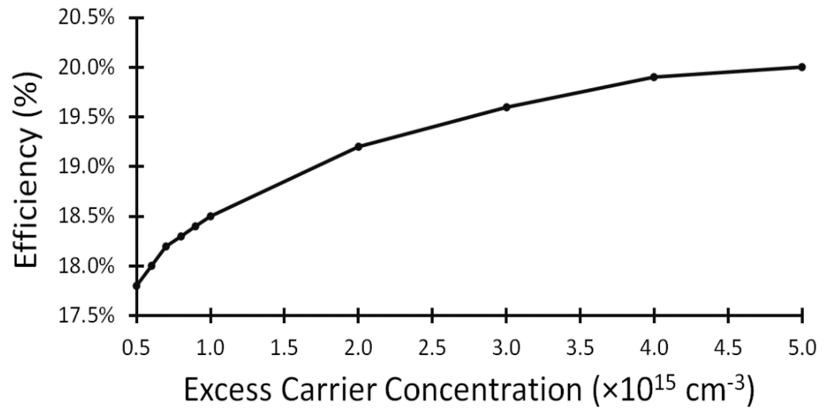
The excess carrier concentration (ECC) has a great effect on the solar cell performance as it determines the open-circuit voltage,
FF, and solar cell efficiency.
Figure 6 shows the effect of excess carrier concentration on the PCE of the solar cell, which increased with the increase in the excess carrier concentration.
The open-circuit voltage,
FF, and PCE are illustrated in
Table 3 for different excess carrier concentrations.
As illustrated in
Table 3, the efficiency is increased with the increase in the excess carrier concentration and reaches 20% for ECC equal to 5.0 × 10
−15 cm
−3. However, the ECC value is strongly related to the effective lifetime of the carriers, where the maximum value of the effective lifetime is 3 ms, which is obtained at ECC = 1 × 10
−15 cm
−3.
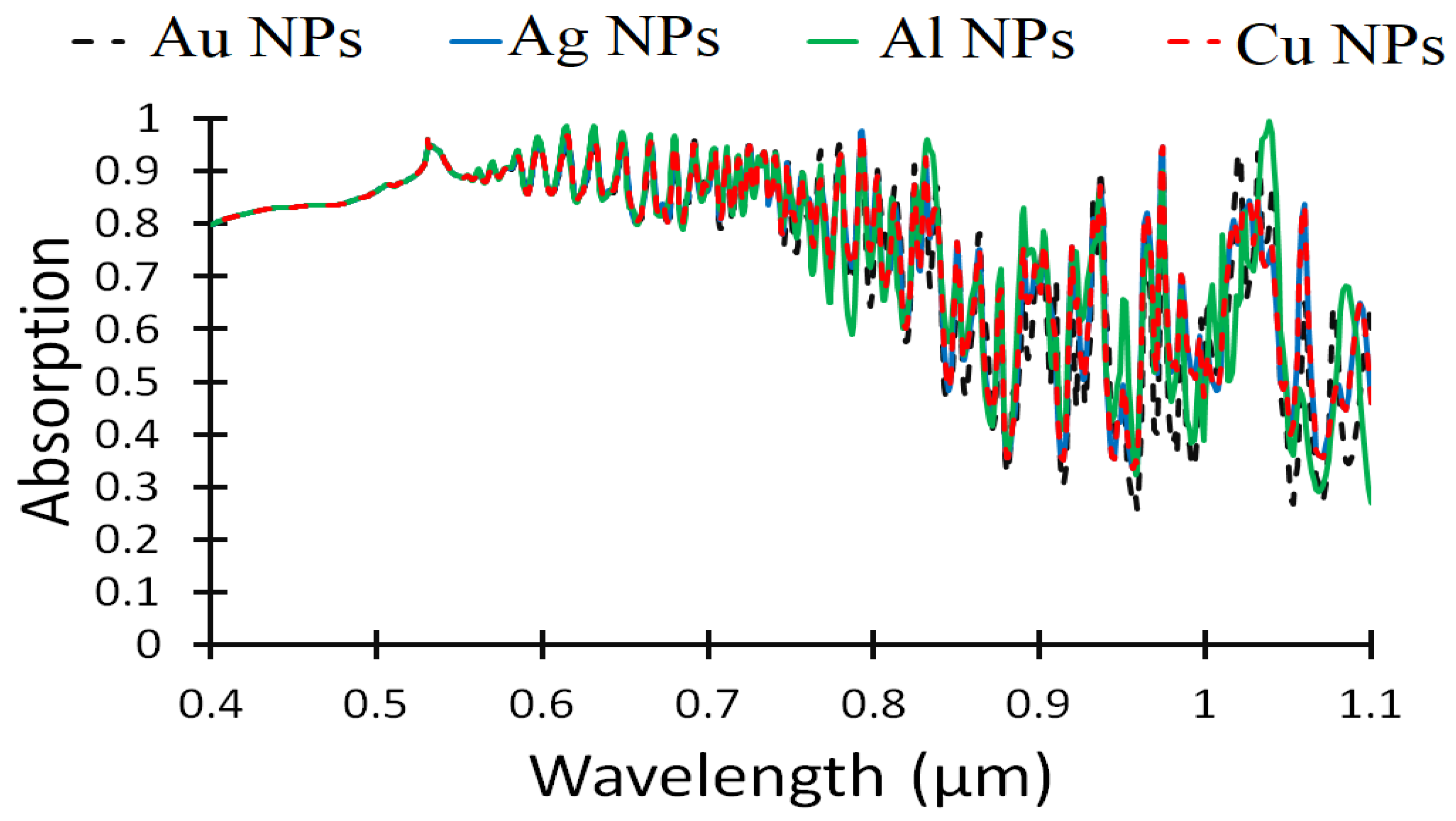
The NP material plays a very important role, as illustrated in Equation (6), which consequently changes the
Jsc and
µ values.
Figure 7 shows the absorbed energy for different NP materials, namely Au, Ag, Al, and Cu. In the visible region, the absorptions of all NP materials are almost the same, very close to each other, and one cannot distinguish between them, so the main factor in determining the best material is the short-circuit current density and consequently the PCE.
Gold NPs produce a high
Jsc and PCE, while silver and copper have
Jsc values equal to 37.6 and 37.4 mA/cm
2, respectively, as clearly given in
Table 4. Aluminum NPs give a short-circuit current density of 33.1 mA/cm
2 and overall efficiency of 15.1%. The maximum obtained power conversion efficiency is 19.0% at short-circuit current density
Jsc = 41.7 mA/cm
2.
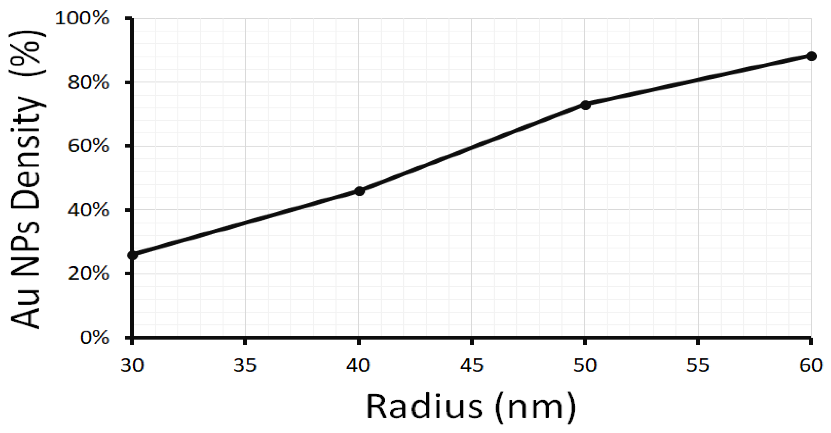
Plasmonic nanoparticle radius is also considered as one of the main factors that affect solar cell performance.
Figure 8 shows the absorbed energy for different Au NP radii, namely 30, 40, 50, and 60 nm. Due to the oscillation of the absorbed power in the NIR region, no distinction between different radii can be considered, so the short-circuit current density is the main factor of choice. The maximum performance,
Jsc of 41.6 mA/cm
2 and
µ of 19.0%, has been obtained at 50 nm Au NP radius, as introduced in
Table 5.
Figure 9 gives the density of the distributed Au NPs (%) for different radii; the maximum performance of the solar cell is obtained at an NP radius equal to 50 nm, as shown in
Table 5.
To calculate the Au NP density, the area of all distributed NPs in the unit cell is divided by the available area on the silicon substrate, without NWs.
The period,
P, between each NW has a significant effect on the solar cell performance. So, the effect of changing the period from 350 to 600 nm on the short-circuit current density and power conversion efficiency is simulated and summarized in
Table 6.
The optimum performance is obtained at period P = 550 nm, which gives Jsc = 41.7 mA/cm2 and PCE = 19.0%. The values of short-circuit current density and PCE decrease as the NW separation distance increases, larger than 500 nm, as the concept of multireflection of the incident light is decreased.
Moreover, the height of the NWs also plays a very important role in solar cell performance. Hence, the effect of NW length on the short-circuit current density and PCE is calculated with a change in the NW length from 3 to 6 µm as given in
Table 7. The best performance has been obtained at 5 µm length, as the increase in the length will increase the electron relaxation due to changing the NW bandgap.
5. Optical Power Distribution
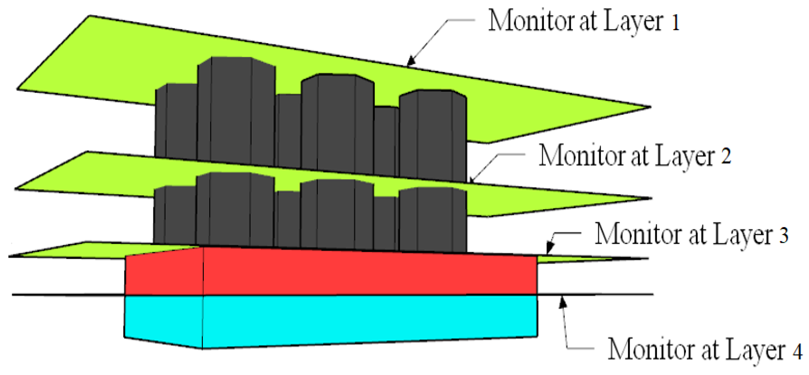
Optical power distribution is monitored at different layers, between the silicon substrate and back oxide, layer 1; at the top of Si substrate, layer 2; in the middle of the SiNWs, layer 3; and at the top of NWs, layer 4.
Figure 10 shows the locations of the four layers.
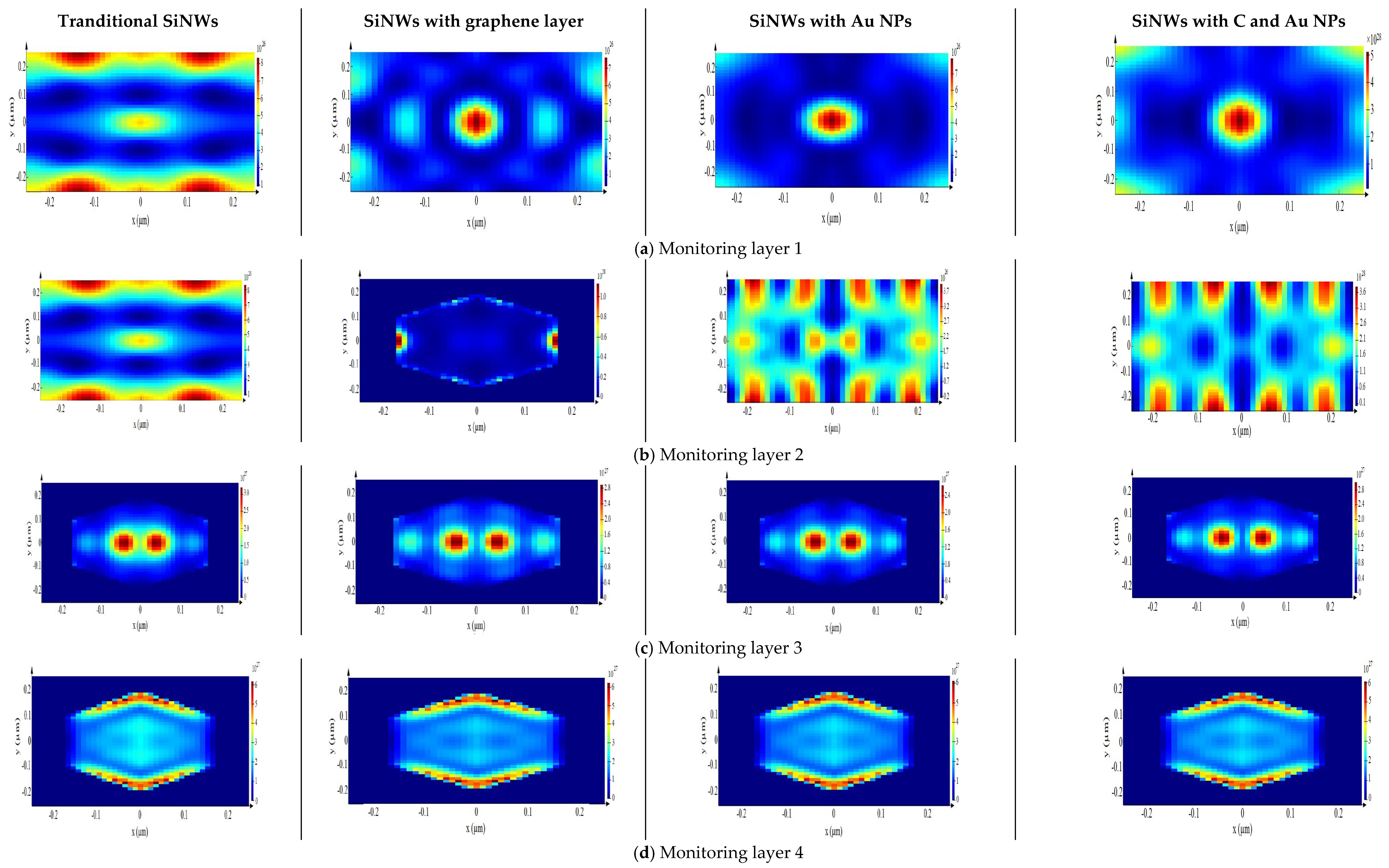
Figure 11 illustrates the optical power distribution on the four different monitoring layers for all proposed solar cells, traditional SiNWs, SiNWs with C layer, SiNWs with AuNPs, and SINWs with C and Au NPs.
Figure 11a, monitoring layer 1, shows the effect of the graphene layer on the top of NWs; it behaves like a nanoantenna, which retransmits the optical power into the active layer. Au NPs absorb the optical power on the substrate surface, as clearly shown in monitoring 2 with Au NPs; however, monitoring layers 3 and 4 have the same effect.
Finally, the proposed solar cell structure is compared to other structures in the literature, fabricated structures as in [
1,
5,
6,
13] and analytical analysis work as in [
14], as illustrated in
Table 8. The proposed structure does not give the maximum open-circuit voltage, 0.63 V, or
FF, 0.73; however, it produces a high short-circuit current density, 41.7 mA/cm
2, and consequently a high value of the power conversion efficiency, 19.0%.
In brief, the main advantage of this study is that the proposed structure enhances the absorption of the SiNWs in the NIR region in addition to the visible region, which leads to improvement in the overall solar cell performance.


