Featured Application
The proposed triple phase shift (TPS) dual active bridge (DAB) resonant converter control scheme is suitable for high-efficiency electrical vehicle (EV) wireless charging applications.
Abstract
This paper presents a new triple phase shift (TPS) closed-loop control scheme of a dual active bridge (DAB) LCC resonant DC/DC converter to improve wireless charging power transfer efficiency. The primary side inverter phase shift angle regulates the battery charging current/voltage. The secondary side rectifier phase shift angle regulates the rectifier AC load resistance to match its optimized setting. The inverter-to-rectifier phase shift angle is set to achieve unity power factor operation of the DAB rectifier and inverter. The mathematical formulation of the TPS shift control is given for each phase shift angle. The analytical calculation, circuit simulation, and experimental test are carried out in a power scaled-down DAB LCC resonant wireless charging converter laboratory hardware setup to validate the proposed TPS close-loop control scheme. The PLECS circuit simulation shows that DAB LCC resonant SiC MOSFET operates at zero-voltage-switching (ZVS) with a unity power factor in emulated constant current (CC) mode battery charging. In constant voltage (CV) mode operation, one inverter/rectifier Leg does not operate at ZVS switching when Sic MOSFET is switched on near zero current. The experimental results show that the efficiency is greatly improved for CV mode charging with large DC load resistance connected if rectifier AC load resistance matching control is enabled. The measured efficiency matches well with the analytical calculation. The estimated efficiency improvement will be much more significant for EV applications in the kW power range with greater winding loss. The challenges and possible solutions to implement TPS PWM modulation in two separate inverter and rectifier control hardware are explained for future TPS control algorithm development in practical wireless charging products.
1. Introduction
Wireless power transfer has gained popularity over the years as this technology can charge electric vehicles (EVs) without requiring a power cable and a plug-in connector. In recent years, inductive power transfer by a DC/DC resonant converter has become an effective wireless charging method [1]. For EV wireless charging applications, the considerable variation of wireless transformer parameters exists practically due to the significant magnetic coupling factor change caused by air-gap distance variation, the misalignment between the transmitter and the receiver pads, and the receiver coil parameter vehicle-to-vehicle variation. For the basic series-series (S-S), series-parallel (S-P), parallel-series (P-S), and parallel-parallel (P-P) resonant circuit topologies, the resonant frequency is sensitive to the magnetic coupling factor variation and the receiver coil parameter variation. The high-order LCC resonant circuit is a more appealing topology for its robustness to the resonant circuit parameter variation and battery operation condition variation [2,3,4].
The resonant frequency selection is an important design decision for a wireless charging system. High resonant frequency improves the magnetic coupling and reduces the size of the wireless charging transformer. Therefore, increased resonant frequency reduces winding loss, core loss, and shield loss. The cost for high frequency is increased power device switching loss [5]. SiC MOSFET in the market’s 600 V~1700 V voltage range opens the opportunity to implement high resonant frequency for EV wireless charging systems. Compared to SI MOSFET devices, SIC MOSFET has the advantage of much smaller and thermal-stable On-resistance Rds, which leads to low conduction loss. The intrinsic fast diode in SIC MOSFET has a much lower reverse recovery charge (Qrr) (low switching-off loss). SIC MOSFET is an ideal choice for wireless charging DC/DC resonant converter, which runs at hard-switching control with acceptable power device loss in low current at CV battery charging mode [5]. The switching loss of Sic MOSFET is estimated to reduce to around 50% with ZVS switching. The ZVS switching can be realized by introducing a phase shift between inverter/rectifier AC voltage and current so that the turn-off current at MOSFET switching ON transition is large enough to discharge the MOSFETs junction capacitors within dead time [6,7].
For a conventional unidirectional wireless charging system, the battery current or voltage feedback control is implemented in the transmitter side high-frequency DC/AC inverter, and the receiver side AC/DC converter is an uncontrolled diode rectifier bridge. The loss distribution of a unidirectional 8 kW wireless charging MOSFET DC/DC LCC resonant converter is estimated as 52.3% from transmitter and receiver coils, 16.7% from LCC compensation network, 11.9% from power MOSFETs, 16.8% from rectifier diodes, and 2.2% from output filter [2]. Similar power loss distributions are reported in [8] in CC mode charging operation. For wireless charging systems, the loosely coupled transmitter and receiver coils dissipate most of the power loss because of a relatively larger resonant current [2,8].
In LCC resonant compensation parameter design calculation, inverter AC circuit zero-phase-angle (ZPA) constraint is imposed to minimize reactive power flow into AC resonant circuit and maximize LCC resonant circuit efficiency [2,9,10,11] The resonant compensation circuit design with inverter ZPA operation constraint is critical for achieving high-efficiency operation of the wireless charger at CC charging mode with low battery equivalent resistance. However, resonate circuit efficiency significantly degrades in CV charging mode operation when battery equivalent load resistance is significantly increased [12,13,14].
Intensive research efforts are published to minimize the efficiency degradation caused by battery equivalent resistance variation in CV battery charging mode. This research effort can be generally classified as load impedance estimation and load impedance matching control, which requires modifying the rectifier side circuit and implementing dual side control of the DC/DC resonant converter. A simple solution is to add a post-regulation DC/DC converter after the diode rectifier to regulate the effective load impedance of the resonant circuit when the battery charging condition is changed. In [14], dynamic maximum-efficiency tracking control is proposed for S-S resonant converter wireless charging system by adding a pre-regulation DC/DC converter before the inverter on the transmitter side and a post-regulation DC/DC converter after the diode rectifier on the receiver side. On top of battery voltage/current/power regulation in inverter control, the duty cycles for pre-regulation DC/DC converter and post-regulation DC/DC converter are adjusted based on “perturb & observer” methods to minimize the measured efficiency. In [15], a post-regulation buck-boost converter is added after the diode rectifier bridge for the LCC resonant converter wireless charging system. The diode rectifier output DC load resistance is regulated around a reference load resistance value by duty cycle control of the buck-boost converter to improve efficiency in CV charging mode operation. The CC/CV/power regulation is realized in inverter control using model-based power/current calculation from the estimated inverter AC load resistance. In [16], a pre-regulation buck converter is added before the inverter. A semi-active rectifier replaces the diode bridge. The battery charging current is controlled by rectifier side phase shift PWM modulation with voltage pulse synchronized with measured receiver coil current. The inverter phase shift angle is kept at maximum value. The buck-boost duty cycle is adjusted to optimize the system efficiency based on the “perturb & observer” method. The drawback of this extra pre/post-DC/DC converter solution is that the efficiency improvement is compromised by the power loss generated by the additional power circuit. The wireless charging system also becomes more bulky, costly, and less reliable.
Recently, intensive research interests are raised in using DAB resonant converter control to improve the efficiency of the wireless charging system by simply replacing the diode bridge with an active rectifier bridge [7,17]. The advantage of DAB resonant converter topology is that it does not increase power device component count and opens the possibility to use low loss Sic MOSFET devices. For the DAB DC/DC resonant converter, it is crucial to ensure that both the inverter and rectifier work in ZPA conditions to minimize the reactive power input and output to the resonant circuit. The resonant compensation circuit design based on inverter ZPA constraint was originally developed for unidirectional DC/DC resonant with the diode rectifier. The underline assumption for unity power factor operation of the inverter is that the resonant circuit output has a purely resistive load. However, DAB resonant converter control can operate the active rectifier bridge in either a capacitive or inductive power factor by advancing or delaying the rectifier AC voltage relative to the current. It is essential that DAB DC/DC resonant converter control takes care of pure resistance AC load assumption and ensures that the DAB rectifier bridge operates at unity power factor for the DAB inverter bridge operating at ZPA condition. This restriction on DAB resonant converter control freedom has yet to be explained and discussed in publications.
In [7], the method to implement triple phase shift (TPS) control of the DAB LCC resonant converter wireless charging circuit is reported. The input/output current/voltage waveform relationship is utilized to derive the inverter phase shift angle βp and rectifier phase shift angle βs according to the load power demand. The inverter-to-rectifier phase shift angle is set to δ = 90° + ∆δ with ∆δ calculated analytically from the discharging current of the power electronic switch, the resonant circuit parameters, and the input/output DC voltage to maximize the ZVS operation range of the inverter and rectifier bridges. The robustness performance of this TPS control method is questionable because it is challenging to obtain accurate circuit parameters for the inverter and rectifier phase shift angle online calculation in a practical wireless charging system.
In [17], a phase-lock-loop (PLL) based double phase shift control scheme is proposed for a DAB S-S resonant converter wireless charging system. The inverter phase shift angle controls battery charging voltage/current. The rectifier phase shift angle controls the effective AC load resistance of the resonant circuit. A PLL algorithm was proposed to adjust the rectifier voltage window based on the zero-crossing detection of the receiver winding current to achieve closer to zero reactive power operation of the rectifier AC circuit. The PLL timing synchronization control algorithm implicitly adjusts the inverter-to-rectifier phase shift angle. The inverter ZPA can be realized with rectifier-side PLL timing synchronization control. It is hard to understand rectifier-side PLL auto-tuning results concerning inverter AC voltage and current because the inverter-to-rectifier phase shift angle for this DAB S-S resonant converter needs to be analyzed and evaluated. An explanation needs to be given about how the PLL algorithm starts to work in DC/DC converter power-on the startup process when there is current in the resonant circuit.
This paper presents a detailed TPS closed-loop control implementation method on DC/DC LCC resonant converter for the wireless charging system. The battery charging current/voltage feedback control generates the inverter phase shift angle. The rectifier phase shift angle is generated by LCC resonant circuit AC load resistance feedback control to improve the efficiency performance in CV charging operation. The theoretical DAB inverter-to-rectifier phase shift angle, which satisfies the LCC resonant compensation circuit ZPA design constraint for unity power factor operation of the inverter, is derived from the equivalent LCC resonant circuit model. The inverter-to-rectifier phase shift angle is set to δ = 90° for unity power factor operation of the DAB inverter and rectifier. The possible methods for TPS control implementation in decoupled inverter and rectifier control hardware are explained for future engineering development in wireless charging products. The simulation and measurement study results are discussed in the conclusion section.
2. DAB DC/DC Resonant Converter TPS Close Loop Control Scheme
2.1. DAB DC/DC Resonant Converter TPS PWM Modulation
DAB DC/DC resonant converter has a symmetrical circuit structure. It is suitable for the bi-directional operation of a wireless charging system at a single resonant frequency with high-power density and high efficiency.
Figure 1 shows the wireless charging DAB LCC resonant DC/DC converter circuit with transmitter side H-bridge DC/AC inverter and receiver side H-bridge AC/DC active rectifier. The function description of the symbols denoted in Figure 1 is given in Table 1. In this paper, Rac_out is the study focus for rectifier side control and is denoted as “Rac”.
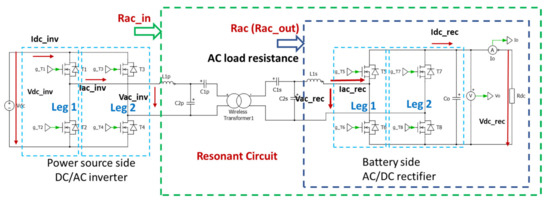
Figure 1.
Wireless charging DAB LCC Resonant DC/DC resonant converter.

Table 1.
DAB LCC resonant converter circuit notation definition.
Figure 2 illustrates the triangle PWM carrier signals, the PWM gating signals of the top switches of the inverter and rectifier Legs, and the resulting AC voltage waveforms of the inverter and rectifier for DAB TPS PWM modulation. The same color is used for signal notation and the signal itself.
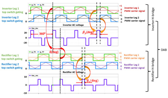
Figure 2.
Inverter and rectifier AC voltage pulse generation from DAB TPS PWM modulation.
The PWM carrier signals generate the PWM gating signals. The gating signal for the bottom switch has the opposite polarity as the top switch of the same Leg. A turn-on delay is applied for all gating signals to generate a dead time to prevent short-through fault of the inverter and rectifier Leg. The inverter and rectifier AC voltage waveforms are generated by the inverter and rectifier PWM gating signals.
Table 2 listed out phase shift angles with their PWM carrier signal sources and the results shown in inverter/rectifier AC voltage waveforms. The phase shift time between two Legs is defined as the period between positive zero-crossings of the PWM carrier signals for the two Legs. The phase shift time is converted to phase shift angle in degree, with the ratio of one PWM cycle 360°.
Table 2.
DAB Phase Shift Angle Generation and Results.
The magnitude of the inverter/rectifier AC voltage pulse is the same as its corresponding DC voltage. The polarity of phase shift angle δ determines the power flow direction of the bidirectional DAB converter. For DAB LCC resonant converter, the optimized inverter-to-rectifier phase shift angle δ = 90° with inverter AC voltage leads the rectifier AC voltage to achieve unity power factor operation of the DAB converter for battery charging. The detailed derivation process will be given in Section 2.2.2.
In the real-time control algorithm implementation, the values of phase shift angle βp, βs, and δ are normalized over 3600 (one PWM switching period) as βp = βp (deg)/360, βs = βs (deg)/360, and δ = δ (deg)/360.
2.2. Mathematical Formulation of DAB TPS Control Method
2.2.1. Charging Power Regulation with Inverter Phase Shift Control
Using Fourier series expansion of the inverter AC pulsing voltage as explained in [18,19,20], the inverter steady state AC RMS voltage fundamental frequency component can be expressed as (1) as a function of the inverter phase shift angle βp and DC voltage. When phase shift angle βp = 0.5 (βp (deg) = 180°), the inverter voltage waveform becomes a square waveform with maximum inverter AC RMS voltage, as shown in (2).
The fundamental resonant frequency component of inverter and rectifier AC RMS voltage and AC RMS current can be decomposed into real and imaginary components in the phasor diagram. With power loss from switching devices ignored, the inverter’s DC power equals its AC power.
The averaged DC input power can be expressed as a product of the inverter’s AC RMS voltage, AC RMS current, and the inverter power factor, as shown in (3), where is the power factor angle of the inverter AC output.
Substituting (1) into (3), the averaged inverter DC input current can be calculated from (4). If the resonant compensation circuit is designed to operate the inverter at ZPA condition with , the relationship of the inverter averaged DC input current and its AC output current is simplified as (5).
Equation (1) means that inverter output voltage can be regulated through inverter phase shift angle for a given fixed inverter DC input voltage. The inverter AC current reflects the battery charging current, the rectifier operation condition, and the resonant circuit operation condition.
Equations (4) and (5) show that DAB input DC current or power is decided by the inverter AC current loading and inverter shift angle. Equations (4) and (5) establish the foundation for battery charging power regulation in constant current (CC) mode or constant voltage (CV) mode using inverter phase shift control.
2.2.2. Resonant Circuit Load Resistance Regulation with Rectifier Phase Shift Control
Using Fourier series expansion on rectifier AC pulsing voltage generated by phase shift PWM modulation, the relationship of rectifier DC voltage and AC RMS voltage can be derived as (6). Applying rectifier input AC and output DC power are balanced with power device loss ignored, the rectifier AC input RMS current and averaged output DC current is derived as (7), where is rectifier AC input power factor angle.
If the rectifier PWM gating signals are disabled, the body diodes of the rectifier H-bridge devices will work as a diode rectifier. In this case, βs = 0.5 (βs (deg) = 180°). The relationship of DC vs. AC RMS voltage/current of the diode bridge rectifier is further simplified as shown in (8) and (9).
For DAB resonant converter with rectifier phase shift control, the AC load resistance of the resonant circuit is the rectifier AC resistance (Rac), which can be derived as (10) from (6) and (7).
For rectifier unity power factor operation, the relationship of rectifier AC and DC equivalent resistance is further simplified as (11), where Rdc = Vdc_rec/Idc_rec is the equivalent battery resistance.
Figure 3 illustrates significant equivalent battery load resistance variation in a typical CC-CV mode battery charging operation. The battery CC or CV charging mode is decided by the battery state of charge (SOC) and the battery voltage level. When the battery voltage is much smaller than its nominal value, and the battery SOC is low, the maximum charging current is applied for CC mode charging. When the battery voltage is approaching its nominal value, and the battery SOC is approaching 100%, the charging current is greatly reduced, and the battery works in CV mode charging.
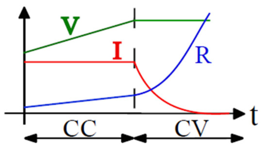
Figure 3.
Battery equivalent resistance variation in CC-CV charging operation.
The load resistance of the DAB resonant converter is the equivalent battery resistance which varies significantly from CC to CV mode charging operation. For DAB resonant converter, according to Equation (11), it is possible to modify the AC load resistance of the resonant circuit by regulating the rectifier phase shift angle βs to improve power efficiency in battery CV mode charging operation.
2.2.3. Inverter-to-Rectifier Phase Shift Angle Setting for Unity Power Factor Operation of DAB LCC Resonant Converter
In TPS PWM modulation signal waveform shown in Figure 2, the inverter-to-rectifier phase shift angle δ is defined as the phase angle difference between inverter voltage and rectifier voltage as expressed in (12).
The inverter-to-rectifier phase shift angle δ setting for unity power operation of DAB LCC resonant converter bridges can be derived from the equivalent LCC resonant circuit model with inverter ZPA constraint for compensation circuit design applied.
Figure 4 shows the equivalent LCC AC resonant circuit connected to the wireless charging transformer. The parameters for Lm, Lrp, Lrs, R1, and R2 are mutual inductance, primary winding leakage inductance, secondary winding leakage inductance, primary winding resistance, and secondary winding resistance. Zac is the resonant circuit load impedance generated by rectifier control. Zac_in is the inverter AC load impedance.
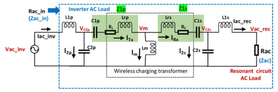
Figure 4.
Equivalent LCC AC resonant circuit with detailed wireless charging transformer parameters.
In the LCC resonant circuit design, the assumption is made that unity power factor operation can be achieved in rectifier control. The rectifier voltage and current are in phase with Zac = Rac. The LCC resonant circuit parameters are designed to meet the resonant requirement (13) and (14) and inverter ZPA operation constraints (15) and (16) as explained in [2,9]. The LCC resonant circuit compensation design ensures that with the unity power factor operation of the rectifier, the LCC resonant circuit compensation parameters are designed to achieve inverter ZPA operation with Zac_in = Rac_in.
Assuming the wireless charging transformer parameters for the transmitter and receiver coils are identical (Lrp = Lrs = Lr, R1 = R2 = R). The LCC resonant compensation circuit is symmetrical with L1p = L1s = L1, C1p = C1s = C1, and C2p = C2s = C2. The impedances of LCC AC resonant circuit components can be expressed as (17) to (22).
The frequency constraint (13) and (14) is re-written as (23) in component impedances. The inverter ZPA constraint (15) and (16) is re-written as (24) in component impedances.
Utilizing KVL and KCL rule, with constraints (23) and (24) applied, the AC currents and AC voltages of the LCC resonant circuit branches are derived as a function of rectifier AC voltage as shown from (25) to (34).
Under the condition that the rectifier operates at unity power factor with Zac = Rac, the inverter-to-rectifier phase angle δ is derived as (35).
Equation (35) proves that the rectifier voltage phase should lag the inverter voltage phase by 90° for DAB LCC resonant converter to operate at unity power factor.
DAB resonant circuit topology affects the inverter-to-rectifier phase shift angle δ setting for inverter and rectifier unity power factor operation. For other DAB circuit topologies, the inverter-to-rectifier phase shift angle for unity power factor operation needs to be derived from the equivalent resonant circuit model.
2.2.4. DAB LCC Resonant Converter Rectifier AC Voltage Phase Measurement from Receiver Coil Current
For LCC resonant converter, the receiver coil voltage and current are sinusoidal signals at resonant frequency, and the phase relationship between transformer winding voltage and current can be utilized to measure the phase rectifier AC voltage at resonant frequency. The resonant frequency component of rectifier AC voltage can be derived as (36) utilizing resonant condition (14), which means that the phase of rectifier AC voltage lags the receiver coil current by 90°.
2.3. DAB TPS Close Loop Control Scheme for Unity Power Factor Operation of Inverter and Rectifier at Optimized Resonant Circuit AC Load Resistance
Figure 5 shows the proposed TPS control scheme to achieve unity power factor operation of the DAB converter at optimized resonant circuit AC load resistance in the wireless charging system. The battery charging voltage/current feedback control is implemented to control the inverter phase shift angle βp. The resonant circuit AC load resistance Rac feedback control is applied to regulate the rectifier phase shift angle βs. The inverter-to-rectifier phase shift angle δ is set to 90° for unity power factor operation of the DAB inverter and rectifier bridges.
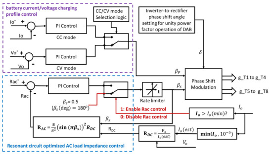
Figure 5.
DAB resonant DC/DC converter TPS control scheme.
The inverter phase shift angle βp changes the inverter AC output voltage pulse-width and the input AC voltage of the resonant circuit so that the power from the inverter to the rectifier can be regulated. In CC mode control, the battery current feedback is applied to regulate the power from the inverter to the rectifier. In CV mode control, the battery voltage feedback is applied to regulate the power flow from the inverter to the rectifier.
For the inverter phase shift control, in CC mode battery charging operation, the DC/DC converter DC output current is regulated around the charging current reference by the proportional and integral (PI) control. The feedback current is the battery charging current measured after the load side filter capacitor. In CV mode charging, the DC/DC inverter output voltage is regulated around the target voltage. The feedback voltage is measured as the battery DC voltage.
The rectifier phase shift control regulates the resonant circuit AC load resistance Rac to match its optimized value. In the control algorithm implementation, the Rac feedback signal is calculated as a function of the rectifier phase shift angle βs and DC load resistance using (11), assuming the rectifier runs at unity power factor. The DC load resistance signal is estimated from the ratio of battery voltage over battery charging current. When the charging current is approaching zero, Rac feedback control is disabled because DC load resistance (Rdc) estimation is inaccurate. In this condition, the rectifier phase shift angle is set to its maximum value at βs = 0.5 and βs (deg) = 180. The change rate of the rectifier phase shift is limited to smooth out the dynamic transition caused by the phase shift command sudden change.
The proposed DAB resonant DC/DC converter TPS close loop control scheme can be implemented for all DAB resonant circuit topologies. However, the optimized AC load resistance value and the optimized inverter-to-rectifier phase shift angle setting to achieve unity power factor operation are to be decided by both the resonant circuit topology and the resonant circuit parameter.
2.4. DAB LCC Resonant Converter TPS Control Performance Design Analhysis
Table 3 shows the wireless charging transformer configuration and parameters. The transformer turns ratio is 1:1. The transmitter and receiver coil parameters are identical. Table 4 shows the design requirement specification. The nominal AC load is calculated from the nominal DC load resistance for the diode rectifier operation. Table 5 shows the LCC circuit parameters from the design calculation using the method given in [12].
Table 3.
Transmitter (Tx) and receiver (Rx) parameters.
Table 4.
Design requirement for LCC resonant converter.
Table 5.
LCC resonant compensation network parameters.
The LCC resonant circuit design analysis assumes that the rectifier is operating at βs(deg) = 180° with unity AC power factor with battery equivalent resistance change. The method presented in [12] is applied for the LCC resonant circuit performance calculation. The switching loss and conduction loss of power electronic switches are ignored in the calculation.
Figure 6 shows the frequency sensitivity analysis of DC transconductance gain for the DAB DC/DC converter vs. the power factor angle of the DAB inverter bridge. The transconductance gain is defined as the ratio of the DC/DC converter DC output current vs. DC input voltage. It decides the DAB converter DC current output capability in CC mode charging. The benefit of the fixed AC load resistance from rectifier phase shift control is that DC/DC converter DC current output capability will not be affected by the mutual coupling factor variation in CC mode charging operation.
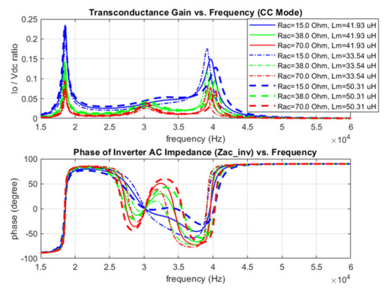
Figure 6.
DC transconductance gain and inverter power factor angle with respect to DAB switching frequency change.
Figure 7 shows the frequency sensitivity analysis of DC voltage gain for the DAB DC/DC converter vs. the inverter power factor angle. The voltage gain is defined as the ratio of the DC output voltage vs. DC input voltage, and it decides the DC/DC converter DC voltage output capability. The DC voltage gain variation is significant due to the AC load resistance change and relatively minor due to the mutual inductance change. The benefit of the fixed AC load resistance from rectifier phase shift control is that the DC voltage gain variation will be significantly reduced in battery CV mode charging application.
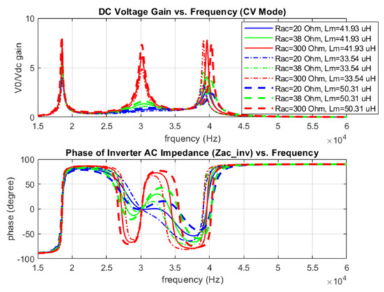
Figure 7.
DC voltage gain vs. inverter power factor angle with respect to DAB switching frequency change.
Figure 8 shows DC input/output voltage/current calculated at different inverter phase shift angle βp (deg) settings vs. AC load resistance change. This result shows that DC output voltage and current magnitude at the same AC load resistance value change significantly with inverter phase shift angle βp (deg). The inverter phase shift angle can be applied to regulate the charging voltage and current in CC or CV mode charging operation. If the AC load resistance can be fixed to Rac (norm) = 38 Ω using rectifier phase shift βs regulation, the maximum output voltage and maximum input and output currents are limited to smaller value ranges.
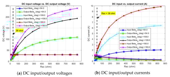
Figure 8.
DC input/output voltages/currents vs. AC load resistance change.
Figure 9 shows DC input and DC output power and power transfer efficiency calculated at different βp (deg) under AC load resistance change conditions. This result shows that DC input and output power change with inverter phase shift angle βp (deg). However, the efficiency does not change with the inverter phase shift angle βp (deg). If Rac = 38 Ω can be achieved with rectifier phase shift control, the maximum input and output power are limited to a smaller value range. Theoretically, the power efficiency can be kept above 86% for all battery operation conditions when the power switching device loss is ignored.
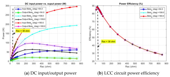
Figure 9.
DC input/output power and efficiency vs. AC load resistance change.
2.5. DAB LCC Resonant Converter TPS Control Implementation in PLECS RT Box
The working principle of the phase shift PWM modulator has been explained in the previous section in the contents related to Figure 2.
Figure 10 shows the FPGA-based triple phase shift PWM modulator connection and configuration for PLECS RT box implementation. The PLECS RT BOX library PWM modulator with variable modulation index inputs, variable frequency ratio input, and variable phase shift angle inputs are used to implement this triple phase shift PWM modulation. The frequency ratio is set to “1” to operate the inverter and rectifier at a single resonant frequency. The symmetrical triangle PWM carrier signals in the range of [−1 1] are configured for the PWM modulator. The modulation index signals for all inverter and rectifier legs are set to zero to generate 50% duty cycle gating signals. The phase shift value settings for all inverter and rectifier Legs are all referenced to the phase of the PWM carrier signal of the inverter Leg 1. The phase shift of the PWM carrier signal between inverter Leg 1 and Leg 2 is Beta_p (βp). The phase shift of PWM carrier signals between rectifier Leg 1 and Leg 2 is Beta_s (βs). Rectifier Leg 1 and Leg 2 PWM carrier signal phase will shift together of delta (δ) phase angle relative to the inverter Leg 1.
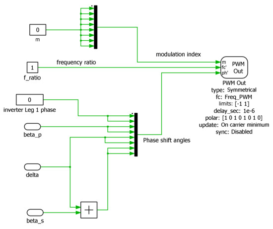
Figure 10.
PLECS-RT BOX phase shift PWM modulator signal connection and configuration.
Figure 11 shows inverter phase shift angle βp generation in the PLECS RT box for experimental test purposes. In the wireless charging system’s regular operation, automatic CCCV mode switching is selected to decide CC and CV mode based on comparing the measured battery voltage with the CV mode threshold and hysteresis threshold as given in (37).
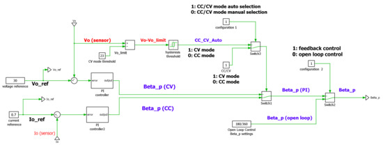
Figure 11.
Inverter phase shift angle βp generation in PLECS RT Box for experimental testing purpose.
Manual CC and CV mode switching can also be configured to individually test out the dynamic performance of the CC/CV mode controller. A configuration switch is added to enable/disable the CC/CV feedback control to test DAB converter performance for inverter phase shift angle open loop control.
Figure 12 shows the rectifier phase shift angle βs generation in the PLECS RT Box real-time control for experimental test purposes. The DAB DC output voltage Vo (Vdc_rec) and current Io (Idc_rec) are measured from current/voltage sensors. The sensor measurement signals are sampled to the PLECS RT box through its high-speed individual 10 bits +/−10 V ADC convention. Before starting of TPS control, the current and voltage sensor signals are calibrated with sensor scaling and sensor offset applied. The voltage sensor ADC sampling result is calibrated for the voltage sensor scaling and offset using differential voltage probe measurement. The current sensor ADC sampling result is calibrated for the current sensor scaling and offsets using the current probe measurement.
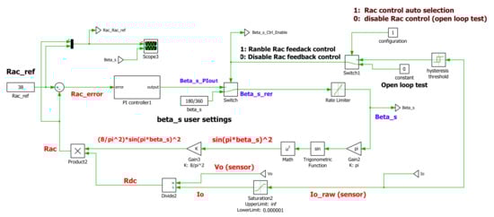
Figure 12.
Rectifier phase shift angle βs generation in PLECS RT Box for experimental testing purpose.
In real-time control at “k” sample, the DC output charging current sensor signal in the unit of “A” at “k” sample is obtained as “Io_raw (k)”; the DC output battery charging voltage sensor signal in the unit of “V” is obtained as “Vo (k). A low limit saturation function is applied on the battery current measurement to avoid divided-by-zero error, as shown in (38). The estimated Rdc signal is constructed using (39)
The rectifier AC resistance signal “Rac” (LCC AC load resistance) is calculated using (40), which is a digital implementation of Equation (11). In Equation (40), βs (k − 1) is the rectifier phase shift angle of the previous sample generated by the “Rac” proportional-integral (PI) feedback controller.
The configuration switches are added to enable/disable the “Rac” feedback control to test DAB performance in open loop control manually βs setting condition. In wireless charging regular operation, Rac feedback control is automatically enabled/disabled depending on the battery current hysteresis threshold settings as given in (41).
The rate limiting for rectifier phase shift angle is applied to smooth out the DAB converter dynamic transition caused by sudden phase shift angle change as given in (42).
2.6. DAB LCC Resonant Converter Open Loop TPS Control Simulation Analysis
2.6.1. DAB LCC Resonant Converter TPS Control with Active Rectifier Control to Achieve Diode Bridge Rectify Performance
Figure 13 shows the PLECS circuit simulation results comparison TPS phase shift PWM modulation with βs (deg) = 180° vs. diode rectifier operation.
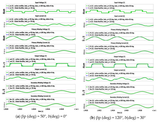
Figure 13.
Inverter/rectifier and transformer voltage and current waveforms with TPS open loop control settings to match diode bridge rectifier performance.
The above simulation results are obtained in DAB open loop TPS control with manual βp, βs, and δ settings when both invert side CC/CV feedback control and rectifier side Rac feedback control are disabled. The inverter-to-rectifier phase shift angle δ settings are manually adjusted for DAB open loop TPS control to match the performance of the diode bridge rectifier operation for the given βp settings.
The simulation results show that the diode bridge rectifier’s performance is much closer to the active rectifier with βs (deg) = 180° and a smaller δ (deg) angle setting. Based on the above simulation results, it is possible to estimate the initial inverter-to-rectifier phase shift angle δ (deg) from AC signal measurement in the diode bridge operation at the power-up stage. Therefore, it is possible to start the rectifier phase shift modulation smoothly from TPS control to achieve diode bridge performance when TPS control is to be implemented in separate control hardware installed in the EV car on the receiver side.
2.6.2. DAB LCC Resonant Converter TPS Control for Unity Power Factor Operation
Figure 14 shows the PLECS circuit simulation results of inverter/rectifier voltage/current and the receiver winding voltage/current waveforms obtained from TPS open loop control for the same inverter/rectifier phase shift angle βp and βs settings but different inverter-to-rectifier phase shift angle δ settings.
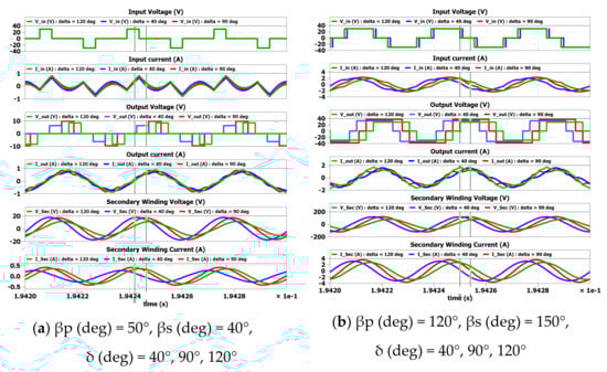
Figure 14.
Inverter/rectifier AC voltage/current and receiver winding voltage/current waveforms for same βp and βs and different δ settings.
These simulation results show that the inverter-to-rectifier phase shift angle δ has a negligible effect on the rectifier AC current waveform. However, it changes the inverter and rectifier power factor angle significantly. The inverter and rectifier operate at unity power factor when the inverter-to-rectifier phase shift angle is around δ = 90°.
In TPS close loop control, the inverter-to-rectifier phase shift angle δ should be automatically adjusted to minimize inverter and rectifier reactive power flow to/from LCC resonant circuit.
2.6.3. DAB LCC Resonant Converter TPS PWM Modulation ZVS Switching Performance
In the power switch ZVS performance study, the circuit simulation needs to be conducted using the circuit parameters and settings of the experimental setup. TPS PWM modulation ZVS switching performance is evaluated in PLECS circuit simulation for SiC MOSFET C3M0120090D with on-resistance Rds = 120 mΩ, output capacitance 40 pF, and SiC MOSFET body-diode forward voltage 4.8 V.
In this study, the DAB DC output resistor is replaced with a DC voltage source from 20 V to 30 V to simulate the battery in different charging conditions. DAB DC input voltage is set to 30 V. The DC output voltage current feedback control is applied to regulate the inverter phase shift angle βp. Rectifier side Rac = 38 Ω feedback control is applied to regulate the rectifier phase shift angle βs. The inverter-to-rectifier phase shift angle is manually set closer to δ = 90°. The PWM gating signal dead time is set to 200 ns.
Figure 15 shows the simulation results when DC output voltage Vo = 20 V and DC output current Io = 0.4 A with δ = 90°. This simulation emulates the condition when Rdc = 50 Ω when the battery is working at the changing CC mode. The simulation results show that inverter/rectifier Leg 1 and Leg 2 are all working at ZVS switching. ZVS soft-switching is achieved when Sic MOSFET is switched on with the freewheeling current flows through its body-diode. In this operation condition, adding an extra inverter-to-rectifier phase with δ = 90 + ∆δ (∆δ > 0) only causes extra reactive power to flow to/from the AC resonant circuit and reduces the power efficiency.
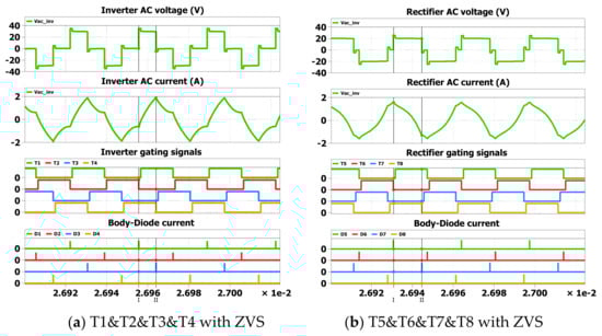
Figure 15.
Inverter/rectifier voltage/current, MOSFET gating signals, diode currents PLECS circuit simulation results for Vo = 20 V, Io = 0.4 A (Rdc = 50 Ω, emulate CC mode) with βp (deg) = 82.3°, βs (deg) = 151, δ (deg) = 90°.
Figure 16 shows the simulation results when DC output voltage Vo = 30 V and DC output current Io = 0.1 A with δ = 90°. This simulation case emulates Rdc = 300 Ω CV mode changing. The simulation results show that inverter Leg 2 and rectifier Leg 1 and Leg 2 work in ZVS switching. Inverter Leg 1 does not work in ZVS switching.
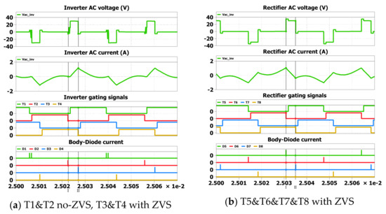
Figure 16.
Inverter/rectifier voltage/current, MOSFET gating signals, diode currents PLECS circuit simulation results for Vo = 30 V, Io = 0.1 A (Rdc = 300 Ω, emulate CV mode) with βp (deg) = 48.3°, βs (deg) = 46.2°, δ (deg) = 90°.
Figure 17 shows the simulation results when DC output voltage Vo=30 V and DC output current Io = 0.1 A with δ = 120°. This simulation emulates Rdc = 300 Ω CV mode battery charging. The simulation results show that after setting δ = 90 + ∆δ with ∆δ = 30° inverter Leg 2 and rectifier Leg 1 and Leg 2 are working in ZVS switching. Inverter Leg 2 is marginally working in ZVS switching.
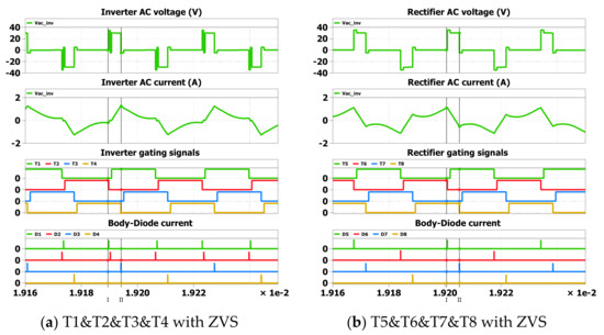
Figure 17.
Inverter/rectifier voltage/current, MOSFET gating signals, diode currents PLECS circuit simulation results for Vo = 30 V, Io = 0.1 A (Rdc = 300 Ω, emulate CV mode) with βp (deg) = 47.065°, βs (deg) = 46.47°, δ (deg) = 110°.
For the proposed TPS closed-loop control, the simulation study shows that when the inverter-to-rectifier phase shift angle is set to δ = 90°, both inverter and rectifier work at ZVS soft-switching mode with unity power factor in CC mode charging. However, in CV mode charging, the inverter-to-rectifier phase shift angle δ needs to increase to meet the ZVS condition. The cost paid is that the inverter and rectifier will deviate from ZPA operation with extra reactive power to/from the resonant circuit, which may increase the loss of the LCC resonant circuit. Further experimental measurement evaluation is required in the practical wireless charging system to decide whether increasing the phase shift delay δ setting is justifiable.
3. DAB LCC Resonant Converter TPS Control Validation
3.1. Experimental Hardware Setups
Figure 18 shows the experimental setup of the DAB LCC resonant converter TPS wireless charging control system. The hardware setup consists of a wireless charging transformer, DAB DC/DC converter built with 900 V, 23 A silicon carbide (SiC) MOSFET C3M0120090D inverter and rectifier bridges, a 1000 μF capacitor on the DC source side, a 2200 μF capacitor on DC load side. A variable resistance load connected to the rectifier DC output emulates the battery charging condition.
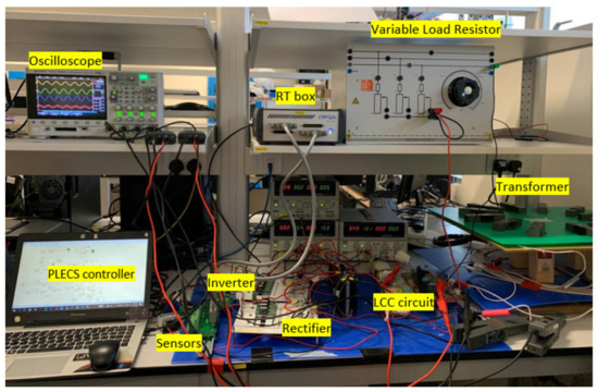
Figure 18.
Experimental setup for DAB LCC resonant converter TPS control system.
DAB LCC resonant converter operates at 30 kHz resonant frequency. SiC MOSFET C3M0120090D has on-resistance Rds = 120 mΩ, source-to-drain capacitance 40 pF, and SiC MOSFET body-diode forward voltage 4.8 V, body-diode reverse recovery charge Qrr = 115 nF, and body-diode reverse recover time 24 ns.
The LCC resonant compensation circuit consists of high-frequency ferrite core inductors and 630 V polypropylene high-frequency high voltage film capacitors. The current and voltage sensor circuit is built with a LEM LA 55-P current transducer and a LEM LV 25-P voltage transducer. PLECS RT box is used as a real-time controller for fast prototyping and experimental validation of the proposed TPS control scheme.
In the experiment test, the input DC power supply voltage is set to 30 V. The inverter-to-rectifier phase shift angle is set to δ (deg) = 90° and rectifier phase shift βs is regulated to meet Rac = 38 Ω in normal TPS close loop operation. When rectifier Rac feedback close loop control is disabled, the rectifier maximum phase shift angle βs = 0.5 (βs (deg) = 180°) is applied. The measurement results are also obtained for different inverter-to-rectifier phase shift angle δ settings to validate the conclusion obtained from the TPS open loop control circuit simulation.
3.2. CC Mode and CV Mode Battery Charging Profile Feedback Control Performance
Figure 19 shows the measurement results for step response of DC output current/voltage for CC/CV mode current/voltage feedback close loop control, respectively, with Rdc = 54 Ω connected. These results validate that the proposed TPS close loop control is stable in the dynamic transition process for CC and CV mode current/voltage feedback control.
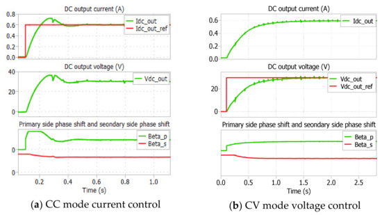
Figure 19.
DC voltage/current step response in CC/CV mode control with = 54 Ω.
3.3. LCC Resonant Circuit AC Voltage and Current Validation in DAB Steady State Operation
Figure 20 and Figure 21 show the inverter/rectifier AC voltage/current waveforms experimental results vs. simulation results in the steady-state operation of the DAB LCC resonant converter. TPS close loop control is regulated at Vo = 10 V and Rac = 38 Ω with Rdc = 56 Ω and Rdc = 200 Ω connected.
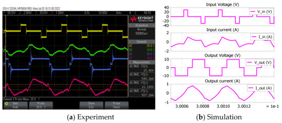
Figure 20.
Inverter/rectifier AC voltage and current waveforms at Vo = 10 V, Rac = 38 Ω with Rdc = 56 Ω connected.
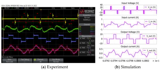
Figure 21.
Inverter/rectifier AC voltage and current waveforms at Vo = 10 V, Rac = 38 Ω with Rdc = 200 Ω connected.
Table 6 compares the measured vs. simulated inverter/rectifier AC voltage and current RMS values for test cases shown in Figure 20 and Figure 21. The RMS values of measurement results match closely with the simulation results for both Rdc = 56 Ω and Rdc = 200 Ω conditions. The phase shift angle βp and βs are greatly reduced for Rdc = 200 Ω, and as a result, the inverter and rectifier AC voltage and current are also reduced for Rdc = 200 Ω.
Table 6.
DAB Inverter/rectifier voltage/current for Rdc =56 Ω vs. Rdc = 200 Ω.
Figure 22 shows another test result for experimental results for inverter/rectifier AC voltage/current waveforms vs. simulation results in the steady-state operation. TPS close loop control is regulated at Vo = 30 V and Rac = 38 Ω with Rdc = 56 Ω connected.
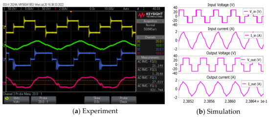
Figure 22.
Inverter/rectifier AC voltage and current waveforms at Vo = 30 V, Rac = 38 Ω with Rdc = 56 Ω connected.
Table 7 compares the measured vs. simulated inverter/rectifier AC voltage and current RMS values for test cases shown in Figure 20 and Figure 22. The RMS values of measurement results match closely with the simulation results for both Vo = 10 Ω and Vo = 30V conditions. The phase shift angle βp is greatly increased for Vo = 30 Ω. The rectifier phase shift angle βs is slightly changed for the same Rdc = 56 Ω connected.
Table 7.
DAB inverter/rectifier voltage/current for Vo = 10 V vs. Vo = 30 V.
3.4. Experimental Results with/without Rectifier AC Load Resistance Feedback Control
Figure 23 shows the experimental results of transmitter coil voltage (Vpri) and current (Ipr), and receiver coil voltage (Vsec) and current (Isec) for CV mode control at Vo = 10 V with Rdc = 150 Ω connected when rectifier Rac = 38 Ω feedback control is disabled vs. enabled.
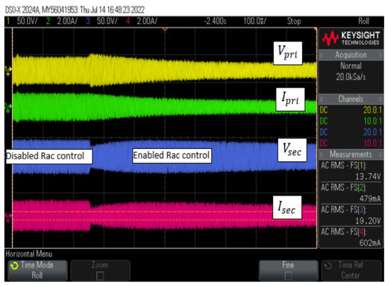
Figure 23.
Transmitter/receiver current/voltage for Vo = 10 V with Rdc = 150 Ω connected when rectifier Rac = 38 Ω feedback control is disabled vs. enabled.
Figure 24 shows the experimental results of transmitter coil voltage (Vpri) and current (Ipri) and receiver coil voltage (Vsec) and current (Isec) for CV mode control at Vo = 40 V with Rdc = 150 Ω connected when the rectifier Rac = 38 Ω feedback control is disabled vs. enabled
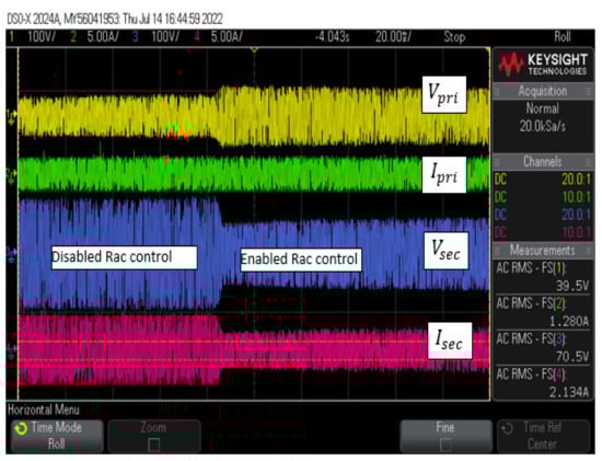
Figure 24.
Transmitter/receiver coil current/voltage at Vo = 40 V with Rdc = 150 Ω connected when rectifier Rac = 38 Ω feedback control is disabled vs. enabled.
Table 8 shows the measured transmitter/receiver winding voltage and current RMS values for Rdc = 150 Ω when Rac = 38 Ω feedback control of rectifier phase shift angle is disabled vs. enabled. The DAB converter operates at Vo = 10 V, 20 V, 30 V, 40 V. These results show that when Rac = 38 Ω feedback control is enabled, the transmitter and receiver current are greatly reduced. Therefore, the transformer winding loss is also significantly reduced.
Table 8.
Transmitter/receiver RMS voltage/current with Rdc = 150 Ω connected.
Figure 25 shows the power efficiency measurement results with Rac = 38 Ω feedback control enabled (solid line) vs. with Rac control disabled (βs = 0.5 and βs (deg) = 180°, dashed line) when different values of Rdc are connected. The measurement is conducted at different DC output voltage (Vo) levels till PI control output is saturated at a maximum phase shift angle of βp (deg) = 180°. The measurement results are plotted as output power vs. power transfer efficiency measured as the ratio of DC output power vs. DC input power.
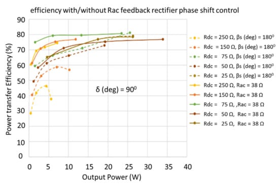
Figure 25.
Power efficiency measurement with/without Rac feedback control.
The measurement data shows that when Rac = 38 Ω control is enabled, power efficiency is greatly improved when a larger Rdc is connected, especially in lower output power operation conditions of DAB. The power efficiency for Rdc = 250 Ω in [1 W, 5 W] output power range is improved from [30%, 40%] to [60%, 75%]. The efficiency variation range is reduced from [30%, 80%] for Rac control disabled to [60%, 80%] with Rac = 38 Ω control enabled.
The maximum power efficiency from measurement data around 80% is slightly lower than 86% shown in Figure 9b obtained from analytical calculation. The reason is that the SiC MOSFET switching loss and conduction loss of the DAB converter have not been included in the analytical calculation.
3.5. Performance Evaluation for Inverter-to-Rectiiver Phase Shift Angle δ Setting Change
In the below experimental test, TPS close loop control performance is measured for different phase shift angle δ (deg) settings to evaluate its effect on power efficiency. This test aims to validate that the DAB should work at δ (deg) = 90° to achieve unity power factor operation and maximum efficiency, as what is proved mathematically in analytical derivation and is validated in PLECS circuit simulation.
Figure 26 shows the measurement data for input DC power vs. phase shift angle δ (deg) change. The DAB converter operates at input DC voltage Vdc = 30 V and output DC voltage Vo = 10 V, 20 V, 30 V, 40 V with different DC load resistor Rdc connected. For the same Rdc and Vo, DC output power is the same; increasing input power means reduced power efficiency.
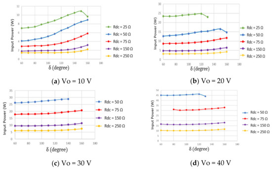
Figure 26.
Input power vs. inverter-to-rectifier phase shift angle δ (deg) when DAB converter operating at Vdc = 30 V and Vo = 10 V, 20 V, 30 V. 40 V with different Rdc connected.
The measurement data show that the input power increases when δ (deg) > 90° for Vo = 10 V and Vo = 20 V for all Rdc values. Therefore, the efficiency will be reduced for a larger phase shift angle δ setting. At higher power levels for Vo = 30 V and Vo = 40 V, the input power is not sensitive to δ (deg) setting change in the range of 80° < δ (deg) < 100°. However, inverter voltage feedback control could saturate at βp = 0.5 and βp (deg) = 180° when δ (deg) > 100° and δ (deg) < 80°.
Based on the above analysis, δ (deg) = 90° is the preferred setting for DAB LCC resonant converter to operate reliability and achieve high efficiency. This conclusion tallies with the conclusion drawn from TPS open loop control simulation results for unity power factor operation of the DAB converter with δ (deg) = 90°.
4. Challenges and Possible Methods to Implement TPS Control in Decoupled Transmitter and Receiver Control Hardware
For the control scheme presented in the previous content, the TPS modulator is implemented in one PLECS RT box control hardware. Therefore, all three phase shift angles can be synchronously controlled by shifting the positive zero-crossing timing instants of the triangle PWM carrier signals of the inverter Legs and the rectifier Legs in the same PWM modulator hardware implemented in the high-timing resolution FPGA.
4.1. Inverter and Rectifier Phase Shift PWM Modulator Implemented in Two Separate Control Hardware
Figure 27 illustrates the inverter phase shift PWM modulators and rectifier phase shift PWM modulation signal connections when the inverter and rectifier phase shift control is to be implemented in two separate control hardware. The initial unknown random inverter-to-rectifier phase shift angle δ_init (random) in the rectifier PWM modulator is generated because of the phase timing difference of inverter Leg 1 and rectifier Leg 1 PWM carrier signals, which cannot be controlled. The inverter-rectifier phase shift angle δ is a control variable which can be adjusted using a self-tuning algorithm for TPS control. The inverter-to-rectifier phase shift angle δ is applied to remove the effect of unknown δ_init and to achieve the desired smooth power-on startup transition performance and unity power factor operation of the DAB converter in regular battery wireless charging operation.
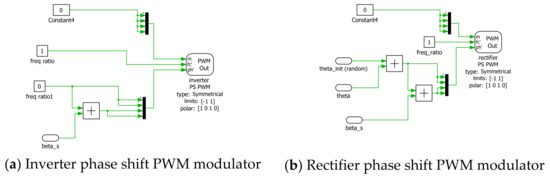
Figure 27.
TPS phase shift PWM modulator signal connections when TPS control in separate inverter and rectifier control hardware.
4.2. DAB Converter TPS Control Smooth Poweron Startup Transition with Inverter-to-Rectifier Phase Shift Angle Auto-Adjustment Scheme
Figure 28 shows the function block diagram for the inverter-to-rectifier phase shift angle δ(deg) auto-adjustment scheme to be implemented in the same high-timing resolution rectifier FPGA of the PWM modulator with two power-on DAB converter startup transition stages added.
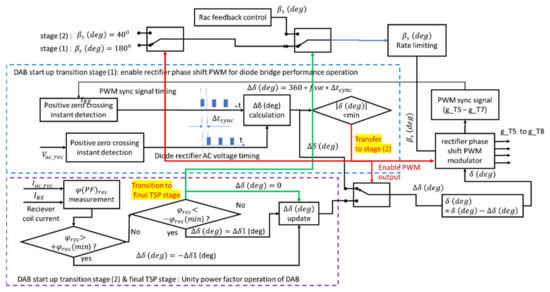
Figure 28.
Function block diagram for DAB smooth startup transition from stage (1) to stage (2) and to the final TPS stage.
The transition stage (1) is to smoothly enable the rectifier phase shift PWM modulator in the DAB converter diode operation condition. The DAB converter power on startup process starts at diode rectifier operation with rectifier side PWM gating signals disabled. The inverter phase shift control is enabled for CC mode operation with a very small charging current to establish the rectifier side AC voltages for diode bridge operation. The rectifier phase shift angle is fixed to βs = 180°. The rectifier PWM carrier signal timing is auto-adjusted to match the diode rectifier timing with the inverter-to-rectifier phase shift angle change. Therefore, the rectifier phase shift control is enabled smoothly from diode bridge operation. Once the rectifier phase shift PWM modulator is enabled, the startup process transfers to the transition stage (2).
The transition stage (2) is to achieve inverter and rectifier unity power factor operation with phase shift angle δ (deg) auto-adjustment. A smaller rectifier phase shift angle is applied in an open loop condition in this stage. The inverter phase shift control operates at the same condition as the transition stage (1). The inverter-to-rectifier phase shift angle is auto-adjusted to minimize the measured rectifier power factor angle to achieve unity power factor operation. Once the DAB converter runs in unity power factor operation, the start-up transition stage (2) is completed, and TSP control is transferred to the regular power transfer operation stage.
4.3. Power on Transition Stage (1)—Smoothly Enable Rectifier Phase Shift Control in Diode Bridge Operation Condition
In the power-on transition stage (1), the rectifier phase shift PWM modulator runs internally when its output gating signals are disabled. The rectifier PWM sync signal is constructed internally in the rectifier PWM modulator FPGA by subtracting the gating signal g_T7 from g_T5. The rectifier phase shift PWM modulator starts with βs (deg) = 180°. The positive zero crossing timing difference of the PWM sync signal and diode rectifier AC voltage is used to auto-adjust δ (deg) setting until ∆δ below its maximum threshold.
Figure 29 shows the operation condition when the positive zero-crossing of the rectifier PWM sync signal aligns with the diode rectifier voltage signal after successful phase shift angle δ(deg) auto-adjustment. In this condition, the rectifier phase shift PWM modulator gating signal output to the bridge power electronic switching devices is enabled. The DAB rectifier bridge phase shift PWM modulation performs similarly to the diode rectifier with smooth power on transition.
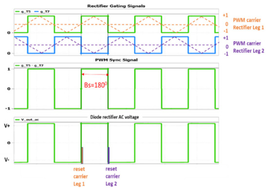
Figure 29.
DAB smooth startup transition stage (1): phase shift angle δ (deg) auto-adjustment for rectifier PWM modulator smoothly enabled in diode rectifier operation condition.
4.4. Power on Transition Stage (2)—Inverter-to-Rectifier Phase Shift Angle Auto-Adjustment for DAB Unity Power Factor Operation in Rectifier Phase Shift Open Loop Control
In the power-on transition stage (2), inverter control is the same as in stage (1). The rectifier shift angle βs (deg) is smoothly reduced through the rate change limiting block to a smaller value setting (for example, βs = 40°) to improve the power factor angle auto-adjustment sensitivity. The rectifier AC power factor angle is measured. The rectifier AC power factor angle is used to adjust δ (deg) to minimize the rectifier AC power factor angle to achieve unity power factor operation of DAB bridges.
Figure 30 shows the block diagram for the rectifier AC power factor angle measurement from phase difference detection of receiver coil AC current and rectifier AC current.
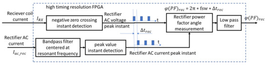
Figure 30.
Rectifier AC power factor angle measurement.
The relationship of the fundamental frequency component of rectifier AC voltage and receiver coil current derived in (36) is rewritten as (43), which means that rectifier AC voltage lags the receiver coil current by 90°. Utilizing (43), the peak instant of the fundamental frequency component of rectifier AC voltage can be detected by the negative zero crossing instant of the harmonic-free receiver coil current.
The high order harmonics of rectifier AC current should be removed by bandpass filter centered at resonant frequency before its peak timing instant detection. The peak instant of the filtered rectifier current can be captured as the phase instant of the rectifier AC current.
The AC power factor angle of the rectifier is calculated from the measured timing error as shown in (44), where “fsw” is the DAB converter resonant and switching frequency. The low pass filtered power factor angle is used for phase shift angle δ auto-tuning adjustment purposes.
Figure 31 illustrates the simulation results of inverter/rectifier AC voltage/current and receiver coil current for different inverter-to-rectifier phase shift angle δ (deg) settings to achieve unity power factor operation. The unity power operation is achieved when the rectifier current peak time instant aligns with the negative zero crossing of the receiver coil current.
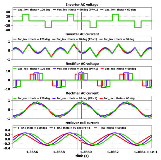
Figure 31.
DAB smooth startup transition stage (2): rectifier δ (deg) auto-adjustment to achieve unity power factor control of rectifier DAB bridge.
4.5. DAB TPS Close Loop Control Stage with Inverter-to-Rectifier Phase Shift Angle Auto-adjustment for DAB Unity Power Factor Operation with Rectifier Feedback Control Enabled
In the power-on transition stage (2), when the rectifier power factor angle is below the threshold setting, the startup process is transferred from stage (2) to the normal TPS closed-loop control stage. In the final TPS control stage, Rac feedback control regulation of βs angle is enabled. The inverter-to-rectifier phase shift angle δ (deg) auto-adjustment for unity power factor operation of DAB continues to run to eliminate the accumulated phase timing draft in either the inverter PWM carrier signal or rectifier PWM carrier signal. The inverter battery voltage and current control are changed to the automatic CCCV mode setting based on battery voltage measurement and SOC status estimation.
5. Conclusions and Discussions
This paper proposes TPS closed-loop control method to realize the unity power factor operation of wireless charging DAB LCC resonant converter at optimized resonant circuit AC load resistance. The efficacy improvement for the proposed TPS control comes mainly from unity power factor operation of the DAB inverter and rectifier. ZVS in CC mode operation helps to improve the efficiency as well. The Rac feedback control improves the efficiency in CV mode charging operation only. One inverter/rectifier Leg may lose ZVS switching in CV mode charging control, which may lower the efficiency at CV mode than CC mode charging.
The analytical calculation of the LCC resonant converter performance using its resonant equivalent circuit model shows that the converter output DC voltage/current and input/output power changes with inverter phase shift angle for the same resonant circuit AC load resistance level. The mathematical analysis provides the theoretical foundation to implement the battery charging current and voltage feedback control with inverter phase shift regulation. The analytical calculation result shows that the AC load resistance of the LCC resonant circuit is another crucial factor which significantly affects the voltage, current, power, and power efficiency of the resonant converter. There is an optimized AC load resistance value for maximum efficiency operation. For a unidirectional LCC resonant circuit with a diode rectifier, the significant variation of equivalent battery load resistance maps into the considerable variation of AC load resistance with a gain factor of . The power efficiency will be degraded when the equivalent battery resistance is significantly increased in CV mode charging. The variation of AC load resistance also causes considerable DC voltage gain variation and inverter load impedance frequency curve shape changes. In DAB TPS control, the low-efficiency issue in CV mode charging can be resolved with AC load resistance feedback control around at optimal target by regulating the rectifier phase shift angle. The ratio of rectifier AC resistance and equivalent battery DC resistance is derived as a non-linear function for rectifier phase shift angle. The AC load resistance is estimated from measured DC load resistance and rectifier phase shift angle to construct the feedback control signal. Lastly, the inverter-to-rectifier phase shift angle for unity power factor operation of the DAB LCC resonant converter is mathematically proven to be δ = 90°. This setting ensures minimizing the reactive power flow in LCC resonant circuit. Therefore, it maximizes the LCC resonant circuit efficiency.
The simulation analysis and experimental test are conducted to validate the performance of the proposed DAB resonant converter high-efficiency control solution. The simulation and experimental results verified that the proposed DAB control system works as designed. DC output voltage and current can be regulated stably around its reference value in either current or voltage feedback control conditions with inverter phase shift control. The unity power factor operation is achieved when the inverter-to-rectifier phase shift angle is δ = 90°. The DAB converter efficiency is significantly improved when rectifier side Rac feedback control is regulated around its smaller normal value when a larger DC load resistance is connected in the test. The transformer winding current magnitude is greatly reduced when Rac feedback control is enabled when larger DC load resistance is connected to DC/DC converter output. The simulation and measurement results for TPS control matches well.
The ZVS performance of TPS control is conducted in the circuit simulation in the simulated CC mode control and CV mode control of battery charging condition by replacing the load resistor with a DC voltage supply to emulate the battery. The simulation results show that Sic MOSFET switches of the inverter and rectifier work at ZVS soft-switching conditions in the emulated CC mode charging with a low battery equivalent load resistance. However, in the CV mode charging with large battery equivalent load resistance, one of the inverter/rectifier Legs may lose ZVS soft switching. This explains why the measured efficiency is still around 20% lower at a smaller power condition with larger DC load resistance connected, even if the Rac control is enabled. From the circuit simulation results, a slight adjustment of inverter-to-rectifier angle may not improve the ZVS switching in CV mode operation.
The proposed TPS control is validated in a small power laboratory experimental setup. The achievable efficiency is from 60% to 80% for the output power range from 1 W to 35 W. The efficiency improvement with Rac feedback control enabled is around 30% at power level from 1 W to 5 W. The total efficiency measurement from this small power wireless charging DAB LCC resonant converter experimental setup is lower than the published efficiency from a large power wireless charging setup. This is because, at a low power level of around 30 W, the small SIC MOSFET switching and conduction loss contribute to a significant percentage of power efficiency reduction. Efficiency improvement from 30% to 60% at 1 W to 5 W power level with Rac feedback control enabled indicates that winding loss is a significant contribution for the wireless charging system even at a very low power level. For kW range, high power EV charging application, the efficiency of the proposed TSP control scheme will be much better than the DAB control solutions published as a result of optimized Rac feedback control and the unity power factor operation of DAB converter bridges resulting from a significant reduction in winding loss in the wireless charging system.
There are some engineering challenges to implementing the proposed TPS closed-loop control scheme in the wireless charging system with separate transmitter and receiver control hardware. The paper provides some basic ideas on how to implement the inverter and rectifier PWM modulation separately. The power-on startup transition stages are required to be added smoothly to enable rectifier side phase shift PWM modulation in diode rectifier operation conditions. The inverter-to-rectifier phase shift angle is to be automatically adjusted to minimize the power factor angle to achieve the unity power factor operation. The feasibility study is done with circuit simulation. However, it requires considerate engineering effort to make the idea work in a suitable wireless charging product.
Author Contributions
Conceptualization, S.C., Y.C., R.T.N. and S.L.; methodology, S.C. and Y.C.; software, S.C. and Y.C.; validation, S.C. and Y.C.; formal analysis, S.C. and Y.C.; investigation, R.T.N. and S.L.; writing—original draft preparation, S.C. and Y.C.; writing—review and editing, S.C., R.T.N. and S.L.; supervision, R.T.N. and S.L. All authors have read and agreed to the published version of the manuscript.
Funding
This research received no external funding.
Institutional Review Board Statement
Not applicable.
Informed Consent Statement
Not applicable.
Data Availability Statement
Not applicable.
Acknowledgments
The authors would like to thank Singapore Institute Technology for the Lab equipment provided for experimental validation.
Conflicts of Interest
The authors declare no conflict of interest.
Abbreviations
The following abbreviations are used in this manuscript:
| DC | Direct current |
| AC | Alternate current |
| CC | Constant current |
| CV | Constant voltage |
| EV | Electric vehicle |
| LLC | Inductor-inductor-capacitor |
| LCC | Inductor-capacitor-capacitor |
| DAB | Dual active bridge |
| Rx | Receiver |
| Tx | Transmitter |
| WPT | Wireless power transfer |
| PLL | Phase lock loop |
| ZPA | Zero phase angle |
| ZVS | Zero voltage switching |
| DPS | Double phase shift |
| TPS | Triple phase shift |
| EMI | Electromagnetic interference |
References
- Ahmad, A.; Alam, M.S.; Chabaan, R. A comprehensive review of wireless charging technologies for electric vehicles. IEEE Trans. Transp. Electrif. 2017, 4, 38–63. [Google Scholar] [CrossRef]
- Li, S.; Li, W.; Deng, J.; Nguyen, T.D.; Mi, C.C. A Double-Sided LCC Compensation Network and Its Tuning Method for Wireless Power Transfer. IEEE Trans. Veh. Technol. 2015, 64, 2261–2273. [Google Scholar] [CrossRef]
- Galigekere, V.P.; Onar, O.; Pries, J.; Zou, S.; Wang, Z.; Chinthavali, M. Sensitivity analysis of primary-side LCC and secondary-side series compensated wireless charging system. In Proceedings of the 2018 IEEE Transportation Electrification Conference and Expo (ITEC), Long Beach, CA, USA, 13–15 June 2018; IEEE: Piscataway, NJ, USA, 2018; pp. 885–891. [Google Scholar]
- Feng, H.; Cai, T.; Duan, S.; Zhao, J.; Zhang, X.; Chen, C. An LCC-Compensated Resonant Converter Optimized for Robust Reaction to Large Coupling Variation in Dynamic Wireless Power Transfer. IEEE Trans. Ind. Electron. 2016, 63, 6591–6601. [Google Scholar] [CrossRef]
- Haque, M.S.; Mohammad, M.; Pries, J.L.; Choi, S. Comparison of 22 kHz and 85 kHz 50 kW wireless charging system using Si and SiC switches for electric vehicle. In Proceedings of the 2018 IEEE 6th Workshop on Wide Bandgap Power Devices and Applications (WiPDA), Atlanta, GA, USA, 31 October 2018–2 November 2018; IEEE: Piscataway, NJ, USA, 2018; pp. 192–198. [Google Scholar]
- Nguyen, B.X.; Singh, J.; Zhang, X.; Jiang, W.; Koh, L.H.; Wang, P. Design and Control for ZVS Constant Current and Constant Voltage Wireless Charging Systems. In Proceedings of the 2018 IEEE 4th Southern Power Electronics Conference (SPEC), Singapore, 10–13 December 2018; IEEE: Piscataway, NJ, USA, 2018; pp. 1–7. [Google Scholar]
- Zhang, X.; Cai, T.; Duan, S.; Feng, H.; Hu, H.; Niu, J.; Chen, C. A Control Strategy for Efficiency Optimization and Wide ZVS Operation Range in Bidirectional Inductive Power Transfer System. IEEE Trans. Ind. Electron. 2019, 66, 5958–5969. [Google Scholar] [CrossRef]
- Qu, X.; Chu, H.; Wong, S.C.; Chi, K.T. An IPT battery charger with near unity power factor and load-independent constant output combating design constraints of input voltage and transformer parameters. IEEE Trans. Power Electron. 2019, 34, 7719–7727. [Google Scholar] [CrossRef]
- Vu, V.-B.; Tran, D.-H.; Choi, W. Implementation of the Constant Current and Constant Voltage Charge of Inductive Power Transfer Systems with the Double-Sided LCC Compensation Topology for Electric Vehicle Battery Charge Applications. IEEE Trans. Power Electron. 2018, 33, 7398–7410. [Google Scholar] [CrossRef]
- Lu, J.; Zhu, G.; Lin, D.; Zhang, Y.; Wang, H.; Mi, C.C. Realizing Constant Current and Constant Voltage Outputs and Input Zero Phase Angle of Wireless Power Transfer Systems with Minimum Component Counts. IEEE Trans. Intell. Transp. Syst. 2021, 22, 600–610. [Google Scholar] [CrossRef]
- Lu, J.; Zhu, G.; Lin, D.; Zhang, Y.; Jiang, J.; Mi, C.C. Unified Load-Independent ZPA Analysis and Design in CC and CV Modes of Higher Order Resonant Circuits for WPT Systems. IEEE Trans. Transp. Electrif. 2019, 5, 977–987. [Google Scholar] [CrossRef]
- Cao, S.; Naing, H.Y.Y.; Naayagi, R.T.; Lee, S.S.; Wei, F.; Tseng, K.J. Wireless charging resonant converter topology study based on analytical design computation. In Proceedings of the 2020 3rd International Conference on Energy, Power and Environment: Towards Clean Energy Technologies, Shillong, India, 5–7 March 2021; IEEE: Piscataway, NJ, USA, 2021; pp. 1–6. [Google Scholar]
- Cao, S.; Nawawi, A.; Lim, Z.; Ang, J.; Hu, X.; Tong, C.F.; Tseng, K.J. Wireless Charging Technologies and Standardization for Electric Unmanned Crafts. In Proceedings of the 2022 International Power Electronics Conference (IPEC-Himeji 2022-ECCE Asia), Himeji, Japan, 15–19 May 2022; IEEE: Piscataway, NJ, USA, 2022; pp. 2147–2154. [Google Scholar]
- Li, H.; Li, J.; Wang, K.; Chen, W.; Yang, X. A Maximum Efficiency Point Tracking Control Scheme for Wireless Power Transfer Systems Using Magnetic Resonant Coupling. IEEE Trans. Power Electron. 2015, 30, 3998–4008. [Google Scholar] [CrossRef]
- Zhao, Q.; Wang, A.; Liu, J.; Wang, X. The Load Estimation and Power Tracking Integrated Control Strategy for Dual-Sides Controlled LCC Compensated Wireless Charging System. IEEE Access 2019, 7, 75749–75761. [Google Scholar] [CrossRef]
- Li, Z.; Huang, X.; Song, K.; Jiang, J.; Zhu, C.; Du, Z. Constant current charging and the maximum system efficiency tracking for wireless charging systems employing dual-side control. In Proceedings of the 2018 International Power Electronics Conference (IPEC-Niigata 2018-ECCE Asia), Niigata, Japan, 20–24 May 2018; pp. 84–87. [Google Scholar]
- Jiang, Y.; Wang, L.; Wang, Y.; Wu, M.; Zeng, Z.; Liu, Y.; Sun, J. Phase-Locked Loop Combined with Chained Trigger Mode Used for Impedance Matching in Wireless High Power Transfer. IEEE Trans. Power Electron. 2020, 35, 4272–4285. [Google Scholar] [CrossRef]
- Ping, W. Modeling and Simulation of Full-Bridge Series Resonant Converter Based on Generalized State Space Averaging. Appl. Mech. Mater. 2013, 347–350, 1828. [Google Scholar]
- Salem, M.; Jusoh, A.; Idris, N.R.N.; Alhamrouni, I. Modeling and simulation of generalized state space averaging for series resonant converter. In Proceedings of the 2014 Australasian Universities Power Engineering Conference (AUPEC), Perth, Australia, 28 September–1 October 2014; IEEE: Piscataway, NJ, USA, 2014; pp. 1–5. [Google Scholar]
- Yang, E.X. Extended Describing Function Method for Small-Signal Modeling of Resonant and Multi-Resonant Converters. Ph.D Thesis, Virginia Tech, Blacksburg, VA, USA, 1994. [Google Scholar]
Publisher’s Note: MDPI stays neutral with regard to jurisdictional claims in published maps and institutional affiliations. |
© 2022 by the authors. Licensee MDPI, Basel, Switzerland. This article is an open access article distributed under the terms and conditions of the Creative Commons Attribution (CC BY) license (https://creativecommons.org/licenses/by/4.0/).