Abstract
These days, the market of wireless communications has developed dramatically. Thus, demand increased with respect to wireless communication terminals that consume less power. Consequently, integration technology for passive elements and circuit module development with respect to ‘Radio frequency systems’ using ‘Micro electro mechanical system’ is becoming a focused topic. Many researchers focused various perspectives in this field. The development of ultra-low operating voltage elements is required in voltage-tunable MEMS-type capacitors, but development for satisfying demands has not occurred. Among many studies, a capacitor with a high tuning range using carrier beams has been proposed by Barki-Kassem and others in 2006. In the proposed study, a high tuning range was generated using a carrier beam when the voltage was applied, passing through the pull-in point and exceeding the controllable range. However, these carrier beams are relatively inefficient because these are applied only in one location and not in several air gaps. Therefore, this study dealt with the optimization of a new MEMS capacitor concept, such as using a total of four beams and by applying a side wall instead of a single carrier beam compared to the previous study. Therefore, in this study, further steps were applied to existing research findings to optimize a new concept MEMS capacitor by applying the side wall instead of a carrier beam. The side wall is the same as the one used in the four-beam example.
1. Introduction
One of the recent trends in wireless communication devices is miniaturization and high precision using MEMS (Microelectromechanical Systems) technology, which can minimize the RF (Radio Frequency) device in accordance with integrating the digital circuits (e.g., planar and non-planar antenna, duplexer, bandpass and lowpass filter, power filter, power dividers, mixer, and amplifiers) of wireless communications [1]. Moreover, the wireless communication market is rapidly growing, and the demand for wireless communication terminals with lower power consumption and small sizes increased; IMT2000 (International Mobile Telecommunication 2000), which is represented by image communication, emerged as the next-generation industrial communication method. Therefore, the technical development of wireless communication devices should be performed as soon as possible in order to establish the technical basis for its own domestic market.
Currently, the core passive component (e.g., inductor, capacitor) development technology of an RF system using MEMS, RF circuit, the integrated technology of developed passive components, and developed VCO (voltage-controlled oscillator) core RF circuit modules for RF circuits has become a focus of research [2,3]. Moreover, the development of a MEMS capacitor that is compact and is a low operating voltage tunable-type device has been requested according to the RF communication technology. However, the specifications of the device were not still developed enough to meet the needs of such a demand at home and abroad. Therefore, the development of capacitor passive elements is urgently needed for applications as the new MEMS technology.
Studies on the MEMS capacitor with a high tuning range are active in overseas areas.
A MEMS variable capacitor having two movable plates loaded with a nitride layer is proposed by Maher Bak and Kassem and Raafat R. Mansour [4]. Moreover, the electrostatically actuated varactor is based on a parallel-plate approach and is best suited for microwave/millimeter-wave applications by Dimitrios Peroulis and Linda P. B. Katehi [5]. A structure that extends the tuning range of MEMS capacitors by at least a factor of eight was proposed by Tommy K. K. Tsang and Mourad N. El-Gamal [6]. According to Nils Hoivik, M.A et al., they proposed a novel design of an electrostatic digitally controllable variable MEMS capacitor constructed using Cronos MUMPS technology and flipchip technology processing [7].
There are many other studies. One of them proposed a simple flat-plate MEMS capacitor with four carrier beams (Maher Bakri-Kassem and Raafat R. Mansour [8]) but these papers were not performed at the level required by the optimization. In addition, the carrier beams were located in the same position in the air gap. Therefore, its tuning range is limited.
In this paper, we introduce an optimized high tuning range MEMS capacitor with a side wall for supplementing these shortcomings.
2. A Novel MEMS Capacitor
Figure 1 shows the schematic diagram of the novel MEMS capacitor and this has not been optimized yet. Figure 1 is the ideal side wall. The cantilever beam’s length of the novel MEMS capacitor is 260 μm and the air gap is 1.25 μm. Its stiffness changes in accordance with the cantilever beam’s deflection when it comes into contact with the side wall when dc voltages are applied. In other words, we applied the side wall to the gradual stiffness increase by using a change in the cantilever’s effective length.
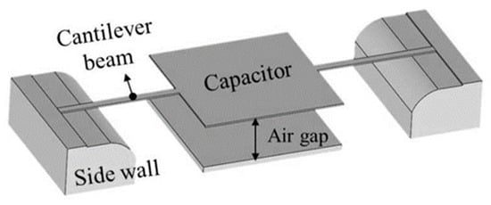
Figure 1.
A schematic diagram of the novel MEMS capacitor.
The location of the stiffness variation is described by the following equation [9].
Carrier beams of number ∞ can be assumed for the side wall, as shown in Figure 2. If vertices of the carrier beams are drawn, that is a profile of the side wall.
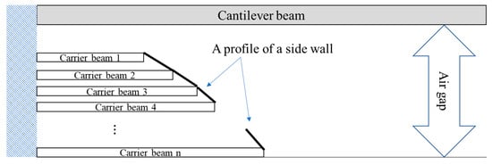
Figure 2.
The assumed side wall.
In this research study, when dc voltages () are applied to the MEMS capacitor, electrical force () is generated according to the number of carrier beams.
Therefore, it can be represented by a single formula as follows.
In this manner, Equation (2), which is n order of the equation, indicates the profile of the ideal side wall. However, in this paper, we demonstrated that the side wall was assumed to be the number of four carrier beams, and we proceeded with the optimization for the side wall.
3. Design Formula
3.1. Design Requirements and Variables
To find the high tuning range of a MEMS capacitor, the objective function is as follows.
Maximize Tuning range
The design variables were selected as , as shown in the Figure 3. Moreover, Table 1 shows the initial values, lower bounds, and upper bounds of each variable.
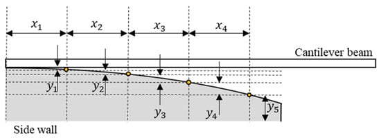
Figure 3.
Design variables of the novel MEMS capacitor.

Table 1.
Initial, lower, and upper limit values of the design.
3.2. Design Problem Formula
The constraints of are divided into four equal parts according to the length of the cantilever beam, measured at (the extra length is set to ), and the constraints of are separated into five equal parts in accordance with air gap; it is distributed at
The following is the design formulation.
| Find | |
| To maximize | Tuning Range |
| Subject to | |
4. Optimal Design
4.1. Analysis Procedures
Figure 4 shows the analysis procedure. This paper used the commercial PIDO (Process Integration and Design Optimization) tool, PIAnO software, by considering the number of design variables and the orthogonality [10].
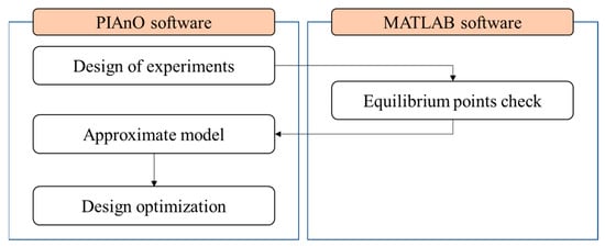
Figure 4.
The analysis procedure.
First, we conducted a design of experiments (DOE) and then the equilibrium points, which include an electrical force and mechanical force nodes for electrical voltage, and they were found according to sampling points by using commercial numerical analysis software MATLAB. Afterwards, approximation models were generated using the Kriging algorithm provided by the PIAnO software. Finally, we derived the optimal solution using a progressive quadratic response surface method (PQRSM).
4.2. Design of Experiments
An orthogonal array has the advantage easy utilization regardless of the lack of a theoretical background. Moreover, the sampling points can be inserted into the array without enlarging the size of the array [11]. Therefore, the orthogonal array of () was conducted by PIAnO, and then we produced graphs of the electrical force and the mechanical force for checking the nodes using MATLAB according to design variables.
4.3. Approximate Model
An approximate model can be approximated for the relationship between performance indices and design variables by using the analysis results at the sampling points specified by a DOE. In this paper, the approximate model-based optimal design, which can be obtained by the optimal solution in a short period of time, was conducted by considering the problem that it requires a long analysis period.
The approximate model was created by Kriging model, since the Kriging model shows superior predictive performance under many design variables and in strongly nonlinear systems. The Kriging model is a type of interpolation model. It was mathematically established by Metheron in 1963 based on research conducted by mining researcher Krige in 1951 [12,13].
Kriging, which shows excellent predictive performances in a system with many design variables and strong nonlinearity, provides statistical estimates.
In addition, there are no custom parameters that rely on the user’s experience or intuition because parameters are optimized via the Maximum Likelihood Estimation (MLE) method [14]. So we selected the Kriging model, which is one of the approximate models provided in the PIAnO software. This Kiriging model was generated by using 27 sampling points, but an accuracy evaluation of underestimated 50% as the accuracy. Then, we remade the orthogonal array () for higher accuracy with respect to the approximate model using the Full Quadratic Polynomial Model. However, this approximate model’s accuracy was also less than 60%. So, to compensate for accuracies, we added 32 sampling points to () using the Argument Latin Hypercube Design (ALHD) method. Therefore, the accuracy of the approximate model increased by using a total of 130 experiment points (sampling points). Finally, in the evaluation results of the metamodel, the accuracy of is over 80%.
4.4. Optimization Technique
The PIAnO tool provides the Progressive Quadratic Response Surface Method (PQRSM) and Evolution Algorithm and micro-Genetic Algorithm (mGA) of optimization techniques. Among them, we used PQRSM by using a direct search optimization. This PQRSM uses sequential approximate optimization algorithms, which uses the concept of a trust region algorithm to guarantee convergence. Moreover, it generates a quadratic response surface model using only the number of 2n + 1 sampling points for the response surface model. It satisfies rotatability, indicating the accuracy of the sampling points; n is the number of input variables. Moreover, PQRSM has the characteristic of a weak global convergence that can find the global optimum via approximation model management using the trust region’s algorithm.
5. Theoretical Analysis
Table 2 shows the optimal design variable values and the initial value. Figure 5 shows the electric force and mechanical force graph in accordance with the optimization value.
Table 2.
Initial and optimal design variables values.
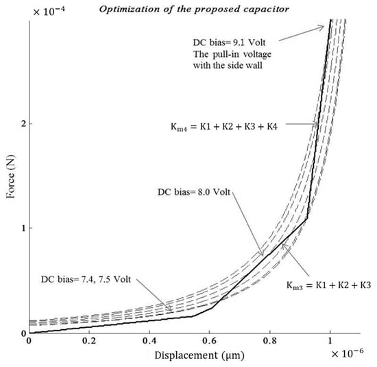
Figure 5.
The electric force and mechanical force graph in accordance with the optimization value.
We confirmed that the displacement value according to the voltage (7.4 V~pull-in point). Table 3 shows the equilibrium points in accordance with electrical force and mechanical force nodes.
Table 3.
Displacement value according to voltage.
The mathematical result is that the conventional research used a pull-in point at 7.4 volts, but the pull-in point of this paper is approximately 9.1 volts. That is, the voltage’s availability increased by about 23%. Moreover, displacement increased by approximately 7% at the pull-in point. Therefore, this novel MEMS capacitor improved the performance by about 30% according to the following expression: .
6. Finite Element Method (FEM) Simulation
To compare the validation of the optimal side wall of the theoretical (mathematical) model and actual model, we performed the finite element method using commercial structure analysis software ANSYS, as shown Figure 6. Therefore, FEM analysis was performed on half of the capacitor for mechanical behavior analyses.
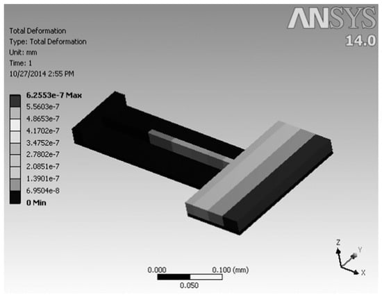
Figure 6.
Static structure the analysis of the optimized capacitor.
Figure 7 represents the displacement result of the comparison with theoretical data and simulations for the mechanical behavior analysis of the optimal MEMS capacitor within the input voltage range from 0 V to 9.5 V.
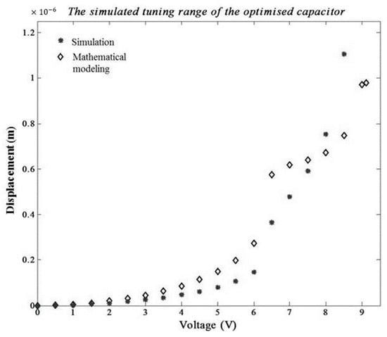
Figure 7.
The displacement result of the comparison according to voltage.
Moreover, there is a difference of data values between 6 and 6.5 volts due to the difference in equilibrium points, which is generated between the displacement and force, as shown in Figure 8.
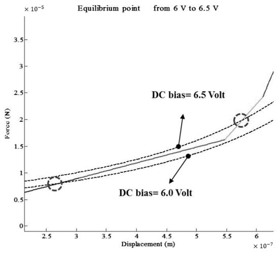
Figure 8.
Equilibrium point from 6 V to 6.5 V.
7. Conclusions
This paper represents a novel MEMS capacitor with a side wall for high tuning ranges. Although various good ideas exist in previously studied cases, there were difficulties with respect to production and cost, and no optimized cases were found.
The following conclusions were obtained by applying the optimized side wall of a novel MEMS capacitor, which is simple and can have a high tuning range.
We conducted side wall optimizations using commercial optimization software PIAnO. Moreover, this paper covered the applicability of the MEMS capacitor by conducting a comparison analysis with a theoretical model using the MATLAB program and a commercial finite element analysis program ANSYS. The pull-in point was generated at approximately 9.12 V on the theoretical result, but the simulation pull-in point was created at approximately 8.5 V. Moreover, the simulation displacement is about 1.1 um, which increased about 12% than the theoretical displacement result.
Currently, this study is an examination of ideas, and it is planned to conduct performance comparison and verification through simulation and in the future.
Author Contributions
Conceptualization, K.L.; data curation, K.L.; formal analysis, K.L.; funding acquisition, J.K.; investigation, K.L.; project administration, J.K.; resources, J.K.; software, K.L.; supervision, J.K.; validation, K.L.; visualization, K.L.; writing—original draft, K.L.; writing—review and editing, J.K. All authors have read and agreed to the published version of the manuscript.
Funding
This research was funded by the National Research Foundation of Korea (NRF) funded by the Korean government (MSIT) (No. 2022R1A2C1005357).
Institutional Review Board Statement
Not applicable.
Informed Consent Statement
Not applicable.
Data Availability Statement
Not applicable.
Conflicts of Interest
The authors declare no conflict of interest.
Abbreviations
| Young’s modulus | |
| Stress of Winding Direction | |
| Width of cantilever beam | |
| Height of cantilever beam | |
| Length of cantilever beam |
References
- Yun, Y. A novel microstrip-line structure employing a periodically perforated ground metal and its application to highly miniaturized and low-impedance passive components fabricated on GaAs MMIC. IEEE. Trans. Microw. Theory. Tech. 2005, 53, 1951–1959. [Google Scholar]
- Varadan, V.K.; Vinoy, K.J.; Jose, K.A. RF MEMS and Their Applications, 1st ed.; Wiley: New York, NY, USA, 2003. [Google Scholar]
- Senturia, S.D. Microsystem Design, 1st ed.; Kluwer Academic Publishers: Boston, MA, USA, 2001. [Google Scholar]
- Bakri-Kassem, M.; Mansour, R.R. Two movable plate nitride loaded MEMS variable capacitor. IEEE. Trans. Microw. Theory. Tech. 2004, 52, 831–837. [Google Scholar] [CrossRef]
- Peroulis, D.; Katehi, L.P. Electrostatically-tunable analog RF MEMS varactors with measured capacitance range of 300%. In Proceedings of the IEEE MTT-S International Microwave Symposium Digest, Los Angeles, CA, USA, 8–13 June 2003; Volume 3, pp. 1793–1796. [Google Scholar]
- Tsang, T.K.; El-Gamal, M.N. Very wide tuning range micro-electromechanical capacitors in the MUMPs process for RF applications. In Proceedings of the 2003 Symposium on VLSI Circuits. Digest of Technical Papers (IEEE Cat. No. 03CH37408), Kyoto, Japan, 12–14 June 2003; pp. 33–36. [Google Scholar]
- Hoivik, N.; Michalicek, M.A.; Lee, Y.C.; Gupta, K.C.; Bright, V.M. Digitally controllable variable high-Q MEMS capacitor for RF applications. In Proceedings of the IEEE MTT-S International Microwave Sympsoium Digest (Cat. No. 01CH37157), Phoenix, AZ, USA, 20–24 May 2001; Volume 3, pp. 2115–2118. [Google Scholar]
- Bakri-Kassem, M.; Mansour, R.R. A high-tuning-range MEMS variable capacitor using carrier beams. Can. J. Elect. Comput. E 2006, 31, 89–95. [Google Scholar] [CrossRef]
- Roy, R.C. Mechanics of Materials, 2nd ed.; Wiley: New York, NY, USA, 2007; p. 796. [Google Scholar]
- PIDOTECH Inc. Process Intergration, Automation, and Optimization. In PIAnO User’s Manual; PIDOTECH Inc.: Seoul, Korea, 2010. [Google Scholar]
- Hedayat, A.S.; Sloane, N.J.A.; Stufken, J. Orthogonal Arrays: Theory and Applications, 1st ed.; Springer: New York, NY, USA, 1999. [Google Scholar]
- Krige, D.G. A Statistical Approach to Some Basic Mine Valuation Problems on the Witwatersrand. J. Chem. Metal. Min. Soc. S. Afr. 1951, 52, 119–139. [Google Scholar]
- Matheron, G. Principles of Geostatistics, Economic Geology. Econ. Geol. 1963, 58, 1246–1266. [Google Scholar] [CrossRef]
- Simpson, T.; Mistree, F.; Korte, J.; Mauery, T. Comparisons of Response Surface and Kriging Models for Multidisciplinary Design Optimization. In Proceedings of the 7th AIAA/USAF/NASA/ ISSMO Symposium on Multidisciplinary Analysis & Oprimization, St. Louis, MA, USA, 2–4 September 1998; Volume 1, pp. 381–391. [Google Scholar]
Publisher’s Note: MDPI stays neutral with regard to jurisdictional claims in published maps and institutional affiliations. |
© 2022 by the authors. Licensee MDPI, Basel, Switzerland. This article is an open access article distributed under the terms and conditions of the Creative Commons Attribution (CC BY) license (https://creativecommons.org/licenses/by/4.0/).