Abstract
We demonstrate, for the first time, GaAs thin film solar cells epitaxially grown on a Si substrate using a metal wafer bonding and epitaxial lift-off process. A relatively thin 2.1 μm GaAs buffer layer was first grown on Si as a virtual substrate, and a threading dislocation density of 1.8 × 107 cm−2 was achieved via two In0.1Ga0.9As strained insertion layers and 6× thermal cycle annealing. An inverted p-on-n GaAs solar cell structure grown on the GaAs/Si virtual substrate showed homogenous photoluminescence peak intensities throughout the 2″ wafer. We show a 10.6% efficient GaAs thin film solar cell without anti-reflection coatings and compare it to nominally identical upright structure solar cells grown on GaAs and Si. This work paves the way for large-scale and low-cost wafer-bonded III-V multi-junction solar cells.
1. Introduction
III-V multijunction solar cells have been the most efficient photovoltaic cells by overcoming the detailed balance limit of single-junction solar cells [1,2,3,4,5]. Recently, six-junction III-V solar cells with three compositionally graded buffers have reached a 1-Sun global efficiency of 39.2% [2]. The monolithically integrated six-junction solar cell requires high material consumption and long epitaxial growth time for the three metamorphic graded buffers that are approximately ~5 μm thick in total. Therefore, the high material growth time and cost can be an obstacle for the use of III-V multi-junction solar cells in various terrestrial applications, other than for space and military applications. Wafer-bonded III-V multi-junction solar cells are another type of high efficiency III-V technology [6,7,8]. Four-junction solar cells fabricated by bonding an InGaP/GaAs dual-junction solar cell to an InGaAsP/InGaAs cell showed a record-breaking conversion efficiency of 44.7% under 297-Suns [9]. Although this approach does not require lengthy and material-consuming growth of metamorphic graded buffers, it must consume two expensive III-V wafers, e.g., GaAs and InP wafers, to create one high efficiency multi-junction solar cell. Since the cost of III-V wafer accounts for more than 80% of the total manufacturing cost [10,11], replacing expensive III-V wafers with cheaper Si wafers could be the first step toward more techno-economic and high efficiency III-V multi-junction solar cells.
Growth of III-V materials on Si, however, creates several hurdles to overcome, such as large lattice mismatch, polar/non-polar growth, and thermal cracks [12,13,14,15,16]. The large lattice mismatch issue can be mitigated via dislocation filter layers, thermal cycle annealing, and two-step growth, while the polarity mismatch can be addressed by using an offcut Si wafer [17,18,19,20,21,22]. The thermal cracks caused by the difference in thermal expansion coefficients during sample quenching can be avoided by restricting the total III-V layer thickness below ~7 μm at moderately low growth temperatures [23]. Decades of research on III-V growth on Si have enabled production of 18.0% efficient monolithic GaAs solar cells on Si by addressing these issues [24,25]. However, the possibility of epitaxial lift-off of III-V solar cells grown on Si for wafer-bonded III-V multi-junction solar cells to reduce their manufacturing cost has not been explored.
Here, we demonstrate, for the first time, a thin-film GaAs solar cell grown on an Si wafer then transferred to a polyimide film via a metal wafer bonding and epitaxial lift-off process. The 2.1 μm-thick GaAs buffer was grown on a Si wafer to reduce the threading dislocation density to 1.8 × 107 cm−2, measured by electron channeling contrast imaging. An inverted GaAs solar cell structure was grown on the GaAs/Si template and revealed a 10.6% 1-Sun efficiency without anti-reflection coating, demonstrating that a wafer bonding and epitaxial lift-off process is compatible with III-V solar cells hetero-epitaxially grown on Si substrates. We believe that an optimized GaAs solar cell structure with InGaP window layer and back-surface field layer will boost the thin film GaAs solar cell performance further.
2. Material Growth
All samples were grown by a Veeco Gen-930 molecular beam epitaxy (MBE) system. Si substrates, with 4-degree offcut towards [110] plane, were used to prevent formation of anti-phase domains. A high-quality GaAs buffer was grown on an Si substrate after desorbing the native oxide at 900 °C for 10 min under As2 overpressure. After oxide desorption, the substrate was cooled to 400 °C for a 100 nm low-temperature GaAs (LT-GaAs) buffer, followed by 400 nm high-temperature GaAs (HT-GaAs) buffer growth at 580 °C. Then, 3× thermal cycle annealing (TCA) was performed at 350~650 °C to increase the dislocation glide velocity and decrease threading dislocation density (TDD). Afterwards, the substrate temperature was raised to 500 °C for the growth of a 200 nm In0.1Ga0.9As single insertion layer (SIL). Subsequently, the 600 nm HT-GaAs was grown at 1 μm/hr, followed by 3× TCA, 200 nm In0.1Ga0.9As SIL, and 600 nm HT-GaAs layer. After the growth of high-quality GaAs buffer, as shown in Figure 1a, electron channeling contrast imaging (ECCI) was performed by Inspect F50 (FEI) to investigate the TDD. The sample was loaded back to the MBE reactor for the growth of GaAs solar cells, as shown in Figure 2a. Cells consisted of inverted GaAs emitter/base structures with Al0.4Ga0.6As window/BSF layers. For the epitaxial lift-off (ELO) process, a 50 nm AlAs sacrificial layer was inserted between the p-GaAs contact layer and the 100 nm GaAs buffer.
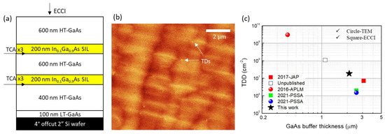
Figure 1.
(a) GaAs buffer structure on 4-degree offcut Si using In0.1Ga0.9As single insertion layer and thermal cycle annealing. (b) An ECCI image of the GaAs buffer surface grown on Si substrate. (c) Threading dislocation density benchmark of GaAs/Si materials reported by other groups.
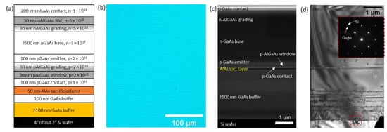
Figure 2.
(a) Schematic illustration of GaAs one-junction solar cell grown on Si substrate. (b) Differential interference contrast optical microscopy image. (c) Cross-sectional SEM image of the entire solar cell structure. (d) Cross-sectional bright-field TEM image. Inset shows the selected area diffraction pattern.
3. Results and Discussion
3.1. Material Characterizations
The total GaAs buffer thickness was maintained at 2.1 μm to avoid thermal cracks in the full device sample because a typical GaAs solar cell adds approximately another 3 μm-thick III-V layers on top of the buffer. Reducing the GaAs buffer thickness typically results in higher TDDs [26]. Therefore, it was important to modify the GaAs buffer structure so that the 2.1 μm-thick GaAs/Si template used in this work could still serve as a virtual substrate with a low TDD. ECCI was performed to investigate the TDD. Figure 1b shows a representative ECCI image where white speckles are individual threading dislocations (TDs) propagating to the surface. The TDDs were calculated by taking more than five images per sample for high statistical accuracy. We achieved a TDD of 1.86 × 107 cm−2 from the 2.1 μm GaAs buffer layer. Figure 1c shows a comparison of TDD in GaAs/Si material system reported by other groups.
Figure 2a shows the schematic structure of one-junction GaAs solar cell grown on Si substrate with optimized TCA and In0.1Ga0.9As SIL. The p-on-n GaAs solar cell has an upside-down structure for metal wafer bonding and ELO process. Figure 2b shows a Nomarski image of the surface with few oval defects and hillocks, which are extremely detrimental to solar cell performance by increasing electrical shunts. The cross-sectional SEM image of Figure 2c reveals the entire GaAs solar cell structure grown on the Si substrate. We also confirmed that the growth of the 50 nm AlAs sacrificial layer for the ELO process did not roughen the layer interface, as seen in the reflection high energy electron diffraction patterns (not shown here). The interfaces in GaAs/Si system were investigated by two-beam condition TEM (Tecnai, FEI) measurement for more clarity to measure the defects. The TEM sample was prepared with Helios G4 HX dual beam (FEI) to make the cross-sections from the actual GaAs buffer on Si. Figure 2d shows a cross-sectional bright field TEM image of the TDs propagating into the GaAs solar cell layer, which were generated at the interface between the GaAs buffer layer and the Si substrate. The compressive strain state of the GaAs buffer was fully relaxed by forming misfit dislocations, as observed in the selected area diffraction image (inset of Figure 2d).
We performed a large area micro-PL on the fully grown sample at room-temperature, as shown in Figure 3a, using a 532 nm green laser as a pump source. The wafer was specular and had no cracks induced by thermal expansion mismatch. Figure 3b shows a 1.5 × 1.5 cm2 PL peak intensity mapping measured from the GaAs layer (λ = ~840 nm), confirming absence of thermal cracks in the fully grown sample. Furthermore, the PL peak intensity varied within a relatively small range from ~3800 to 4200, except for a small spot on the right corner. Raman spectroscopy (In Via Raman Microscope, Renishaw) was also carried out to investigate the strain state of the III-V layer, especially the residual thermal tension (Figure 3c). Five different locations were probed, as shown in Figure 3a, and were compared with the GaAs solar cell sample grown on a GaAs substrate as a reference. Transverse optical phonon peaks at 268 cm−1 and longitudinal optical phonon 290 cm−1 peaks were clearly detected from both [27]. The slight red-shifts from the Si substrate sample compared to the GaAs sample were attributed to the small residual thermal tension in the GaAs epitaxial layer on Si [28]. The excellent homogeneity of material optical property is especially promising for large-scale manufacturing of wafer-bonded multi junction solar cells.
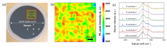
Figure 3.
(a) Photograph of a 2-inch GaAs one-junction solar cell grown on Si substrate. The red-line square shows the selected area for micro-PL mapping. (b) Micro-PL mapping image on the selected area in (a). (c) Raman spectra of GaAs solar cell grown on GaAs and Si substrate.
3.2. Device Fabrication and Performance
Figure 4a shows the fabrication procedure of our solar cells. We first deposited Pt/Au (10/50 nm), which served as a bonding material and ohmic contact metal, on the GaAs solar cell sample and the transfer substrate by electron beam evaporation. Then, standard photolithography was performed to define mesas. The samples were etched using a 1:1:5 mixture of phosphoric acid, hydrogen peroxide, and deionized water for a fast ELO. Subsequently, Ar plasma was irradiated for surface activation, which leaves highly reactive radical site layers that substantially enhance surface adhesion. Metal wafer bonding was conducted with a uniaxial pressure of approximately 40 kgf/cm2. After the bonding process, the GaAs epitaxial layer was separated from the Si donor substrate by an ELO process in which the AlAs sacrificial layer was etched by immersion in HF-based solution [29,30,31]. Finally, Pt/Ti/Pt/Au (20/30/20/200 nm) was deposited on the top contact layers by electron beam evaporation. No anti-reflection coating (ARC) was applied on the cells. Figure 4b shows photographs of the GaAs solar cells transferred to a Pt/Au-coated polyimide film. The inset shows an optical microscope image of the transferred mesa epilayer.
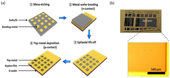
Figure 4.
(a) Fabrication procedure for transfer process of GaAs solar cell. (b) Photograph of transferred GaAs solar cell to polyimide. The inset shows the optical microscope image of GaAs solar cell grown on Si substrate.
Figure 5a shows the sample structures of three different GaAs solar cells: inverted p-on-n GaAs cell grown on Si with AlAs sacrificial layer, upright solar cell, and GaAs solar cell grown on GaAs. The current density (J)-voltage (V) characteristics were investigated to compare the electrical properties of the GaAs solar cells. Figure 5b shows dark J-V curves of the GaAs solar cells and all samples showed good rectifying characteristics with low dark current densities. The comparable dark current densities of 1.26 and 2.08 μA/cm2 between Sample A and B indicated that our ELO process did not degrade the material quality. The inset shows the ideality factor of the GaAs solar cell, which was derived from J-V curves of samples. The ideality factor provides insight on the current flow mechanism; its value is close to 2 when the carrier transport through the p-n junction is dominated by the generation-recombination mechanism. The obtained ideality factor of Sample C grown on a GaAs substrate showed its value to be under 2 at low forward bias voltages, which suggests that the diffusion current was superior over junction recombination current at low forward bias. On the other hand, the ideality factor of Sample A and B showed values above 2 at small forward biases, indicating that the defect-induced recombination and tunneling current was the dominant origin of dark current. Figure 5c shows the J-V characteristics of our fabricated GaAs solar cell in-house under AM1.5G solar spectrum. First, it is of note that our baseline upright GaAs solar cell (Sample C) showed a conversion efficiency of 11.2%. Comparison of the upright GaAs cells grown on GaAs and Si substrate indicated that the presence of 1.8 × 107 cm−2 TDs lowered the open-circuit voltage by 0.13 V and the fill-factor by 7.6%. In addition, Sample B showed a rather lower slope, which was attributed to higher series resistance. The hetero-epitaxial lift-off process seemed to additionally decrease the open-circuit voltage slightly, from 0.79 V to 0.72 V, but it did not affect the fill-factor. Even at low open-circuit voltage, Sample A showed a comparable conversion efficiency of 10.6%, which was slightly smaller than that of the upright cell on GaAs. Moreover, the short-circuit current was increased from 12.1 mA/cm2 to 19.3 mA/cm2, probably due to the light-trapping effect and slight anti-reflection effect of the lift-off etching surface [13,30,31].
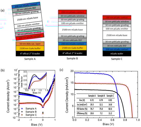
Figure 5.
(a) Schematic diagrams of the one-junction GaAs solar cells. (b) Dark current density (J) −voltage (V) characteristics of GaAs solar cell. Inset shows the ideality factor as a function of bias voltage. (c) J−V curves for fabricated GaAs solar cells.
4. Conclusions
In this work, we demonstrate GaAs thin film solar cells grown on a Si substrate and then transferred to polyimide substrate using hetero-epitaxial lift off. The large mismatch of thermal expansion coefficients between GaAs and Si can generate thermal cracks, but a high quality 2.1 μm-thick GaAs buffer with thermal cycle annealing and In0.1Ga0.9As single insertion layer enabled a thermal crack-free and low threading dislocation density of 1.8 × 107 cm−2. Furthermore, the excellent homogeneity of the material optical property, confirmed by micro-PL and Raman spectroscopy, is especially promising for the large-scale manufacture of wafer-bonded III-V multi-junction solar cells. An inverted GaAs solar cell structure was grown on the GaAs/Si template and revealed a 10.6% 1-Sun efficiency without anti-reflection coatings, demonstrating that a wafer bonding and epitaxial lift-off process may be compatible with III-V solar cells hetero-epitaxially grown on Si substrates. We believe that an optimized GaAs solar cell structure with InGaP window layer and back-surface field layer will boost the efficiency of thin film GaAs solar cells grown on silicon.
Author Contributions
Conceptualization, S.W., D.J. and W.J.C.; methodology, S.W., T.K., N.H. and J.-H.H.; growth, G.R., S.W., D.J. and R.J.C.; fabrication, S.W. and N.H.; analysis, S.W., N.H., D.J., J.B., J.K. and I.-H.L.; writing—original draft preparation, S.W. and D.J.; writing—review and editing, D.J. and W.J.C.; All authors have read and agreed to the published version of the manuscript.
Funding
This research was funded by National Research Foundation of Korea NO. NRF-2017M1A2A2048904, NRF-2021M3H4A1A02051240, and KIST institutional project (2E31011).
Institutional Review Board Statement
Not applicable.
Informed Consent Statement
Not applicable.
Data Availability Statement
Not applicable.
Conflicts of Interest
The authors declare no conflict of interest.
References
- Connolly, J.P.; Mencaraglia, D.; Renard, C.; Bouchier, D. Designing III-V multijunction solar cells on silicon. Prog. Photovolt. 2014, 22, 810–820. [Google Scholar] [CrossRef]
- Geisz, J.F.; France, R.M.; Schulte, K.L.; Steiner, M.A.; Norman, A.G.; Guthrey, H.L.; Young, M.R.; Song, T.; Moriarty, T. Six-junction III–V solar cells with 47.1% conversion efficiency under 143 Suns concentration. Nat. Energy 2020, 5, 326–335. [Google Scholar] [CrossRef]
- Tillmann, P.; Bläsi, B.; Burger, S.; Hammerschmidt, M.; Hoehn, O.; Becker, C.; Jaeger, K. Optimizing metal grating back reflectors for III-V-on-silicon multijunction solar cells. Opt. Express 2021, 29, 22517–22532. [Google Scholar] [CrossRef] [PubMed]
- Li, J.; Aierken, A.; Liu, Y.; Zhuang, Y.; Yang, X.; Mo, J.H.; Fan, R.K.; Chen, Q.Y.; Zhang, S.Y.; Huang, Y.M.; et al. A Brief Review of High Efficiency III-V Solar Cells for Space Application. Front. Phys. 2021, 8. [Google Scholar] [CrossRef]
- Green, M.; Dunlop, E.; Hohl-Ebinger, J.; Yoshita, M.; Kopidakis, N.; Hao, X. Solar cell efficiency tables (version 57). Prog. Photovolt. Res. Appl. 2020, 29, 3–15. [Google Scholar] [CrossRef]
- Cariou, R.; Benick, J.; Feldmann, F.; Höhn, O.; Hauser, H.; Beutel, P.; Razek, N.; Wimplinger, M.; Bläsi, B.; Lackner, D.; et al. III-V-on-silicon solar cells reaching 33% photoconversion efficiency in two-terminal configuration. Nat. Energy 2018, 3, 606. [Google Scholar] [CrossRef] [Green Version]
- Chiu, P.T.; Law, D.C.; Woo, R.L.; Singer, S.B.; Bhusari, D.; Hong, W.D.; Zakaria, A.; Boisvert, J.; Mesropian, S.; King, R.R.; et al. 35.8% space and 38.8% terrestrial 5J direct bonded cells. In Proceedings of the 2014 IEEE 40th Photovoltaic Specialist Conference (Pvsc), Denver, CO, USA, 8–13 June 2014; pp. 11–13. [Google Scholar]
- France, R.M.; Geisz, J.F.; Garcia, I.; Steiner, M.A.; McMahon, W.E.; Friedman, D.J.; Moriarty, T.E.; Osterwald, C.; Ward, J.S.; Duda, A.; et al. Design flexibility of ultra-high efficiency 4-junction inverted metamorphic solar cells. In Proceedings of the 2015 IEEE 42nd Photovoltaic Specialist Conference (Pvsc), New Orleans, LA, USA, 14–19 June 2015. [Google Scholar]
- Dimroth, F.; Grave, M.; Beutel, P.; Fiedeler, U.; Karcher, C.; Tibbits, T.N.D.; Oliva, E.; Siefer, G.; Schachtner, M.; Wekkeli, A.; et al. Wafer bonded four-junction GaInP/GaAs//GaInAsP/GaInAs concentrator solar cells with 44.7% efficiency. Prog. Photovolt. Res. Appl. 2014, 22, 277–282. [Google Scholar] [CrossRef]
- Hadi, S.A.; Fitzgerald, E.A.; Griffiths, S.; Nayfeh, A. III-V/Si dual junction solar cell at scale: Manufacturing cost estimates for step-cell based technology. J. Renew. Sustain. Energy 2018, 10, 015905. [Google Scholar] [CrossRef]
- Kelsey, A.W.; Horowitz, T.R.; Smith, B.; Ptak, A. A Techno-Economic Analysis and Cost Reduction Roadmap for III-V Solar Cells. Natl. Renew. Energy Lab. 2018. [Google Scholar]
- Fan, S.; Jung, D.; Sun, Y.; Li, B.D.; Martın-Martın, D.; Lee, M.L. 16.8%-Efficient n(+)/p GaAs Solar Cells on Si With High Short-Circuit Current Density. IEEE J. Photovolt. 2019, 9, 660–665. [Google Scholar] [CrossRef]
- Hong, N.; Chu, R.J.; Kang, S.S.; Ryu, G.; Han, J.-H.; Yu, K.J.; Jung, D.; Choi, W.J. Flexible GaAs photodetector arrays hetero-epitaxially grown on GaP/Si for a low-cost III-V wearable photonics platform. Opt. Express 2020, 28, 36559–36567. [Google Scholar] [CrossRef] [PubMed]
- Kim, S.; Park, M.-S.; Geum, D.-M.; Kim, H.; Ryu, G.; Yang, H.-D.; Song, J.D.; Kim, C.Z.; Choi, W.J. Fabrication and characterization of single junction GaAs solar cell epitaxially grown on Si substrate. Curr. Appl. Phys. 2015, 15, S40–S43. [Google Scholar] [CrossRef]
- Ryu, G.; Kang, S.S.; Han, J.-H.; Chu, R.J.; Jung, D.; Choi, W.J. Comparative study of metamorphic InAs layers grown on GaAs and Si for mid-infrared photodetectors. Solid-State Electron. 2020, 176, 107942. [Google Scholar] [CrossRef]
- Ryu, G.; Woo, S.; Kang, S.S.; Chu, R.J.; Han, J.-H.; Lee, I.-H.; Jung, D.; Choi, W.J. Optimized InAlAs graded buffer and tensile-strained dislocation filter layer for high quality InAs photodetector grown on Si. Appl. Phys. Lett. 2020, 117, 262106. [Google Scholar] [CrossRef]
- Wang, B.; Syaranamual, G.J.; Lee, K.H.; Bao, S.; Wang, Y.; Lee, K.E.K.; A Fitzgerald, E.; Pennycook, S.J.; Gradecak, S.; Michel, J. Effectiveness of InGaAs/GaAs superlattice dislocation filter layers epitaxially grown on 200 mm Si wafers with and without Ge buffers. Semicond. Sci. Technol. 2020, 35, 095036. [Google Scholar] [CrossRef]
- Mbeunmi, A.B.P.; El-Gahouchi, M.; Arvinte, R.; Jaouad, A.; Cheriton, R.; Wilkins, M.; Valdivia, C.; Hinzer, K.; Fafard, S.; Aimez, V.; et al. Direct growth of GaAs solar cells on Si substrate via mesoporous Si buffer. Sol. Energy Mater. Sol. Cells 2020, 217, 110641. [Google Scholar] [CrossRef]
- Lang, J.R.; Faucher, J.; Tomasulo, S.; Yaung, K.N.; Lee, M.L. Comparison of GaAsP solar cells on GaP and GaP/Si. Appl. Phys. Lett. 2013, 103, 092102. [Google Scholar] [CrossRef]
- Boyer, J.; Blumer, A.; Blumer, Z.; Lepkowski, D.L.; Grassman, T.J. Reduced dislocation introduction in III-V/Si heterostructures with glide-enhancing compressively-strained superlattices. Cryst. Growth Des. 2020, 20, 6939–6946. [Google Scholar] [CrossRef]
- Shang, C.; Selvidge, J.; Hughes, E.; Norman, J.C.; Taylor, A.A.; Gossard, A.C.; Mukherjee, K.; Bowers, J.E. A Pathway to Thin GaAs Virtual Substrate on On-Axis Si (001) with Ultralow Threading Dislocation Density. Phys. Status Solidi 2021, 218, 2000402. [Google Scholar] [CrossRef]
- Jung, D.; Callahan, P.G.; Shin, B.; Mukherjee, K.; Gossard, A.C.; Bowers, J.E. Low threading dislocation density GaAs growth on on-axis GaP/Si (001). J. Appl. Phys. 2017, 122, 225703. [Google Scholar] [CrossRef] [Green Version]
- Yang, V.K.; Groenert, M.; Leitz, C.W.; Pitera, A.J.; Currie, M.T.; Fitzgerald, E.A. Crack formation in GaAs heteroepitaxial films on Si and SiGe virtual substrates. J. Appl. Phys. 2003, 93, 3859–3865. [Google Scholar] [CrossRef]
- Andre, C.L.; Carlin, J.A.; Boeckl, J.J.; Wilt, D.M.; Smith, M.A.; Pitera, A.J.; Lee, M.L.; Fitzgerald, E.A.; Ringel, S.A. Investigations of high-performance GaAs solar cells grown on Ge-Si1-xGex-Si substrates. IEEE Trans. Electron Devices 2005, 52, 1055–1060. [Google Scholar] [CrossRef]
- Wang, Y.; Ren, Z.; Thway, M.; Lee, K.; Yoon, S.F.; Peters, I.M.; Buonassisi, T.; Fizgerald, E.A.; Tan, C.S.; Lee, K.H. Fabrication and characterization of single junction GaAs solar cells on Si with As-doped Ge buffer. Sol. Energy Mater. Sol. Cells 2017, 172, 140–144. [Google Scholar] [CrossRef]
- Wang, G.; Loo, R.; Simoen, E.; Souriau, L.; Caymax, M.; Heyns, M.M.; Blanpain, B. A model of threading dislocation density in strain-relaxed Ge and GaAs epitaxial films on Si (100). Appl. Phys. Lett. 2009, 94, 102115. [Google Scholar] [CrossRef]
- Oda, H.; Inoue, K.; Ikeda, N.; Sugimoto, Y.; Asakawa, K. Observation of Raman scattering in GaAs photonic-crystal slab waveguides. Opt. Express 2006, 14, 6659–6667. [Google Scholar] [CrossRef]
- Sugo, M.; Uchida, N.; Yamamoto, A.; Nishioka, T.; Yamaguchi, M. Residual strains in heteroepitaxial III-V semiconductor films on Si(100) substrates. J. Appl. Phys. 1989, 65, 591–595. [Google Scholar] [CrossRef]
- Kim, T.S.; Kim, H.J.; Geum, D.-M.; Han, J.-H.; Kim, I.S.; Hong, N.; Ryu, G.H.; Kang, J.; Choi, W.J.; Yu, K.J. Ultra-Lightweight, Flexible InGaP/GaAs Tandem Solar Cells with a Dual-Function Encapsulation Layer. ACS Appl. Mater. Interfaces 2021, 13, 13248–13253. [Google Scholar] [CrossRef]
- Woo, S.; Ryu, G.; Kang, S.S.; Kim, T.S.; Hong, N.; Han, J.-H.; Chu, R.J.; Lee, I.-H.; Jung, D.; Choi, W.J. High-Performance Flexible InAs Thin-Film Photodetector Arrays with Heteroepitaxial Growth Using an Abruptly Graded InxAl1–xAs Buffer. ACS Appl. Mater. Interfaces 2021, 13, 55648–55655. [Google Scholar] [CrossRef]
- Geum, D.-M.; Park, M.-S.; Lim, J.Y.; Yang, H.-D.; Song, J.D.; Kim, C.Z.; Yoon, E.; Kim, S.; Choi, W.J. Ultra-high-throughput Production of III-V/Si Wafer for Electronic and Photonic Applications. Sci. Rep. 2016, 6, 20610. [Google Scholar] [CrossRef] [Green Version]
Publisher’s Note: MDPI stays neutral with regard to jurisdictional claims in published maps and institutional affiliations. |
© 2022 by the authors. Licensee MDPI, Basel, Switzerland. This article is an open access article distributed under the terms and conditions of the Creative Commons Attribution (CC BY) license (https://creativecommons.org/licenses/by/4.0/).