1. Introduction
The single-event effect, caused by high-energy charged particles impinging on the sensitive circuits of devices, threatens the stability of space-applied electronic systems. In order to fully understand these single-event effects and predict their effects on circuit systems, sufficient experimental studies and analysis using accelerator tests are required. However, due to the limited availability of heavy ion accelerators and their high cost, the performance of experimental studies has been hindered. Therefore, methods that can replace this method of analysis are gradually being sought and developed in research.
In recent years, the pulsed laser has become a universal testing method for studying microelectronic devices and circuits [
1]. Although the particle accelerator test method is still the standard test for single-event effects, its cost and particle accelerator, which is suitable for the SEE test, can limit the complete characterization of electronic devices and circuits. At the same time, the device is exposed to a high-flux radiation environment in the accelerator test, which destroys the device and leads to the attenuation of its performance. In addition to being more stable and effective, the pulsed laser test also enables the in-depth study of the spatial and temporal characteristics of SEEs, which cannot be achieved by the wide-beam particle test. Similarly, if the pulse laser energy is not particularly high, the device’s damage can be completely avoided. In summary, the pulsed laser single-event effect has become an important testing method, which is a powerful supplement to the heavy ion test method.
Compared with heavy ion accelerators, the perturbation induced by a pulsed laser in electronic devices has the following advantages: the precise control of the spatial and temporal indexes of the injection point, a long time period for its use, and the prospect of effective and low-cost experiments. The process of charge generation induced by the pulsed laser on a semiconductor is a physical process, which is completely different from heavy ion irradiation, which works through the photoelectric effect rather than particle scattering. However, pulsed lasers can also induce SEEs in electronic devices, which can simulate these single-event phenomena caused by heavy ions and establish a relationship between the heavy ion parameters and laser parameters [
2,
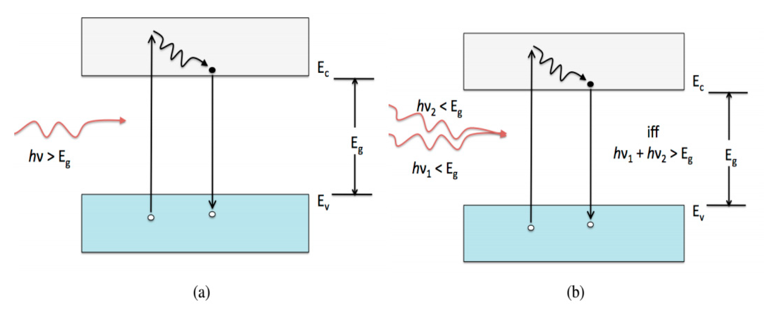
3]. Single-photon absorption (SPA) and two-photon absorption (TPA) are two characterization techniques used mainly for pulsed laser single-event effects. The pulsed laser test is usually carried out by using a laser wavelength above the band gap. The wavelength is above the band gap of the materials, and the photon absorption is mainly based on Beer’s law. That is, when the photon is incident on the semiconductor, each photon absorbed produces an electron hole pair, which is called single-photon absorption [
4]. However, the limiting factor for the selection of this method is that the total penetration of the pulsed laser decays exponentially after it is incident on the surface of the device under test (DUT), which requires that the test should be carried out from the front of the device under test. In this process, the pulsed laser passes through all the material covering the device. As the metal layer of the device increases, pulsed laser testing from the top side becomes difficult or impossible. Because of this limitation, the single-event effect test method of two-photon absorption (TPA) has gradually become the focus of current research.
The TPA test uses a femtosecond pulse laser test with the peak power of the wavelength in the sub-band gap. For light wavelengths lower than the band gap of the semiconductor materials, almost no carriers can be generated at a low light intensity. However, if the laser is strongly focused, the intensity of the incident light is greatest in the region near the focal plane, where the semiconductor material absorbs two photons at the same time, creating an electron hole pair. Based on this theory, the carrier can be injected at any position into the DUT in an accurate way. This method can also avoid the restriction that the carrier cannot be injected due to metal cladding. This method constitutes an important direction for research on the pulsed laser single-event effect test, which was first proposed in 2002 and has been used to characterize the SEE sensitivity of electronic devices and circuits for many years [
5,
6,
7].
In this paper, the single-event transient of an operational amplifier is analyzed using the pulse laser single-photon and two-photon test, further verifying the feasibility of two-photon absorption as a method of single-event effect testing technology.
2. Basic Mechanism
The mathematical models of the pulse propagation and carrier generation in semiconductors are as follows: [
8,
9]
where
I is the pulse laser irradiance,
N is the free carrier density, and φ is the phase. In addition,
α is the single-photon absorption coefficient,
β2 is the two-photon absorption coefficient, which is proportional to the imaginary part of third-order nonlinear optical susceptibility (χ),
β1 is proportional to the real part of χ,
σEX is the absorption rate of laser-induced carriers, and
γ1 represents the refraction of the free carriers. In Formula (3),
is the photon energy, and the coefficient 2 in the denominator of the second term on the righthand side of the formula means that the simultaneous absorption of two photons is required to produce an electron hole pair. In summary, Formula (1) describes the light absorption process as the pulsed laser propagates through the medium, Formula (2) describes the phase change caused by the free carrier and the pulsed laser, and Formula (3) describes the change in the carrier concentration with time due to single photon absorption and two-photon absorption, as shown in
Figure 1. If the selected pulse laser wavelength is in the sub-band gap, the α in the above equation should be equal to 0, in essence, which means that the contribution of single-photon-absorption-induced carriers can be ignored. Then, Formula (3) can be simplified as:
Focusing the laser beam on a small spot enables the formation of a high density of photons in a small area, which can induce the two-photon absorption process.
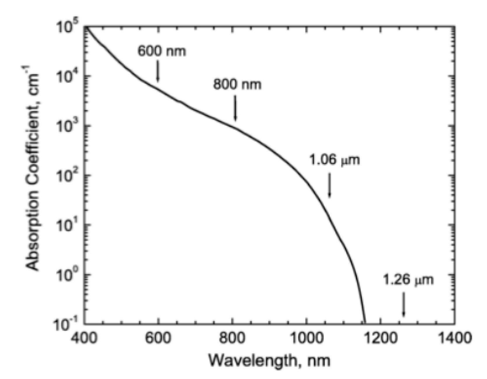
Figure 2, below, shows the absorption spectra of silicon materials at room temperature for different wavelengths of light (visible and near infrared) [
1].
The common wavelengths of the light used in the pulsed laser single-event effect simulation tests are shown in
Figure 2, above. When the wavelength of the light is more than 1200 nm, the linear absorption coefficient can be ignored, which means that, when the wavelength of the light is more than 1200 nm, most carriers are generated by two-photon absorption, and the corresponding energy of one photon is about 1 eV.
This TPA SEE technique has two characteristics that combine to make it particularly useful in SEE testing. Firstly, the pulse test equipment avoids the influences of the top metal layer and device packaging material during the process of the charging of the carriers through the wafer, and there is no exponential attenuation of the light irradiance. Secondly, the quadratic dependence on the irradiance of the pulsed laser restricts the charge carrier to ensure that the maximum light intensity is injected into the confocal region, which makes the charge injection possible at any depth of the material (device).
The two-photon absorption process is different from the single-photon absorption process, which produces a pair of electron hole pairs by absorbing a photon. It is a nonlinear absorption process, and the energy, pulse width, and beam spot diameter of the pulse laser all affect the characteristic parameters of the single-particle effect. When the pulse is prevented from hitting the top of the device, it should hit the inner wafer from the back of the device. For incident from the backside, either the single-photon absorption test method or the two-photon absorption test method can be used. Single-photon absorption and two-photon absorption single-event effects tests also involve different wavelengths.
When the photon energy is greater than the semiconductor band gap (1.12 eV in silicon), it is absorbed directly, resulting in electron hole pairs [
10]. The correlation between the photon energy and light wavelength is [
10]:
where
h is Planck’s constant and c is the speed of light. It can be concluded that the wavelength value of electron hole pair induced in undoped pure silicon is about 1108 nm. For the SPA test method, since the silicon wafer is not very thin, the wavelength is usually selected at 1064 nm, which is sufficiently long to penetrate deep enough to reach the sensitive volume. For the TPA test method, the pulsed laser can pass through the silicon material up to the focal position of the interior in order to induce the generation of carriers. Therefore, by changing the distance between the measured device and the focusing lens, the position of the generation of the carriers can be changed [
11,
12]. At present, the SPA and TPA test methods are commonly used for silicon materials with pulse wavelengths of 1064 nm and 1260 nm. However, SPA technology is not used in SEE tests for wide-band-gap materials, such as SiC, because the photon energy is smaller than the band gap of the material. Therefore, for materials with a wide band gap, the pulse laser wavelength for the TPA test method should vary from 400 nm to 600 nm.
Based on the above analysis, this paper mainly presents experimental research conducted on single-photon absorption- and two-photon absorption-induced single-event effects and offers a comparative analysis.
3. Devices under Test and Setup
3.1. Devices under Test
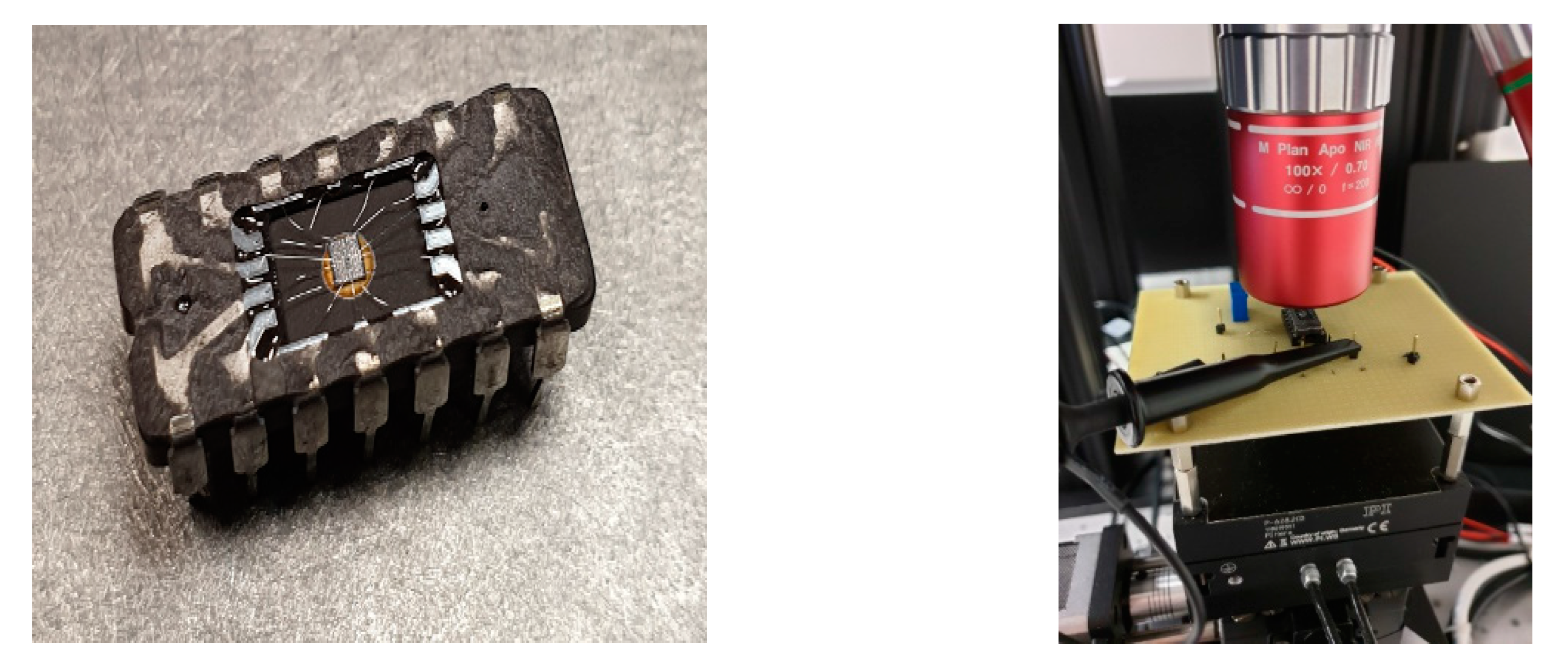
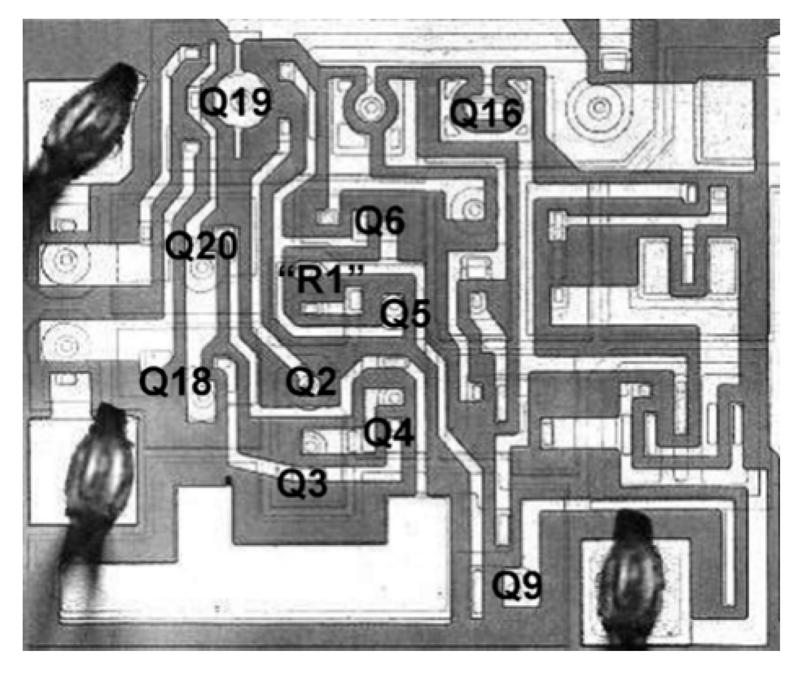
The typical operational amplifier LM124 of the TI company was selected as the device under test, and the single-event transient was induced by a pulse laser. Then, the different characteristics of SPA and TPA were compared and analyzed. Due to the limited penetration capacity of light, the device was capped before the test, as shown in
Figure 3. The device was configured for V = 1 V and V = ±15 V.
3.2. Test Principle and Process
This test is mainly used to obtain the relationship between the transient voltage and the change of the laser focal plane position. The specific test process is as follows:
(1) Determine the zero position of the test:
In experiments with a multiple energy pulse laser test, we must determine for each device being tested an absolute reference position, using the laser position of the device interface of different materials (generally choosing the wafer surface of the device) with a small speckle method in focus, the specific process is a vertically incident laser focused on the surface of the device with the minimum size and maximum intensity of light. We define this position as “zero.” Zero is the absolute position reference of the device under test during each test.
Since the laser spot is visually focused, some errors between the so-called “zero” and the actual interface position are also possible. The principle for determining the laser spot is that the spot has the smallest diameter and the brightest intensity, which corresponds to the most clear reflection caused by the change in the refraction coefficient when the laser beam passes through the covering layer and enters the sensitive area in between. However, since the spot is visibly focused, it is difficult to determine the change in the spot size at the micron level, which means that the error between the zero point and the actual SiO2/Si interface should be at the micron level.
(2) Determine the incident range of the laser scanning area:
For a particular device, once the zero point is determined, the laser incidence range can be defined according to it. Typically, the laser incident range is within a few hundred micronmeters either side of zero.
(3) Irradiate the measured area by moving the laser focal plane in small steps within the range (Z-scanning technology):
After determining the zero point and laser incident range of the device under test, the focal plane of the laser is positioned on one side of the range boundary, and then the focal plane is moved in small steps. The step size varies depending on the device being measured and the diameter of the beam. Typically, the move step is in the range of 0.5–1.0 μm.
(4) Test and record the voltage change in the DUT:
Test the collected voltage in real time after each movement. Specifically, 300 pulses should be recorded after each movement and then averaged at each position point in order to obtain the average at each point.
(5) Obtain the functional relationship of the voltage change with the focal plane:
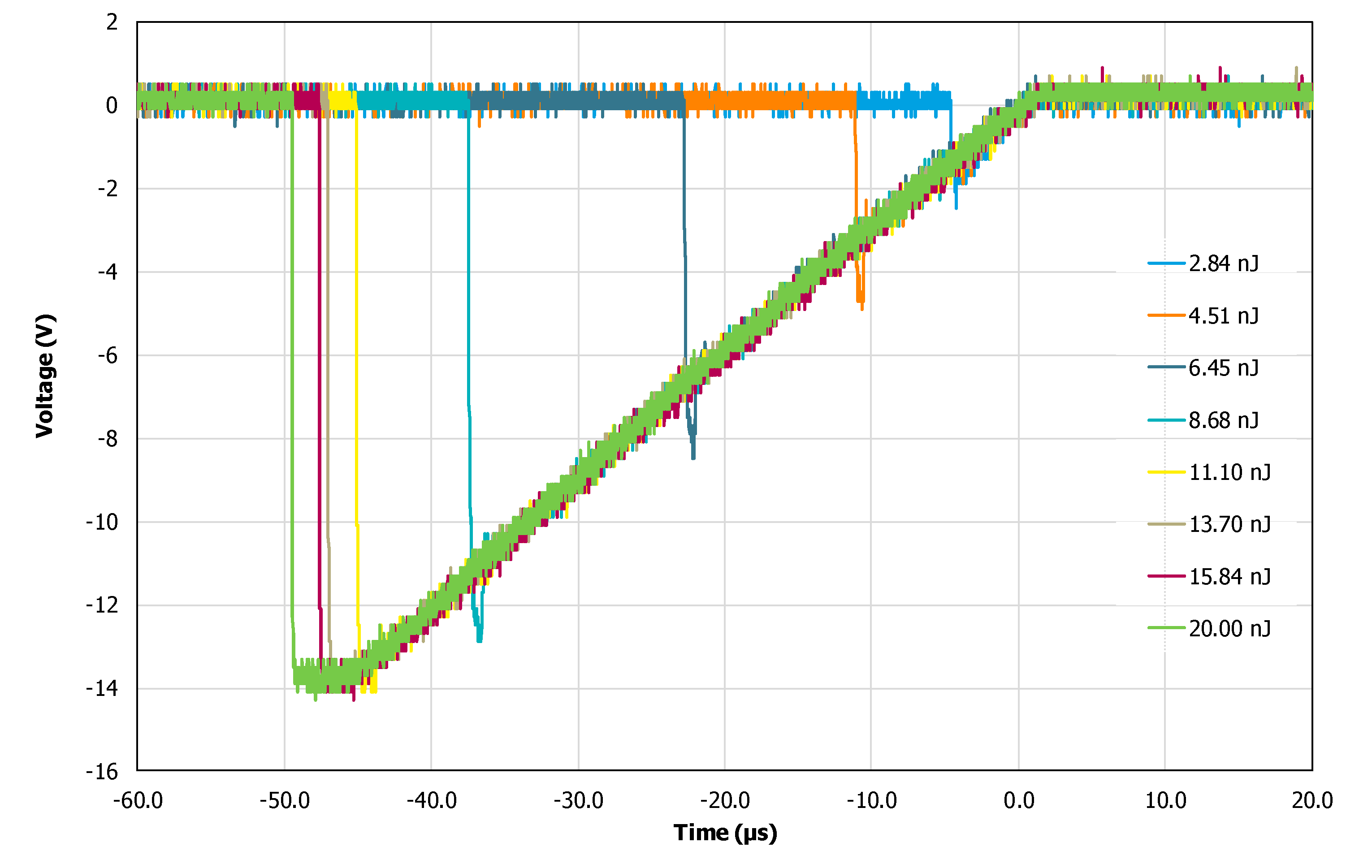
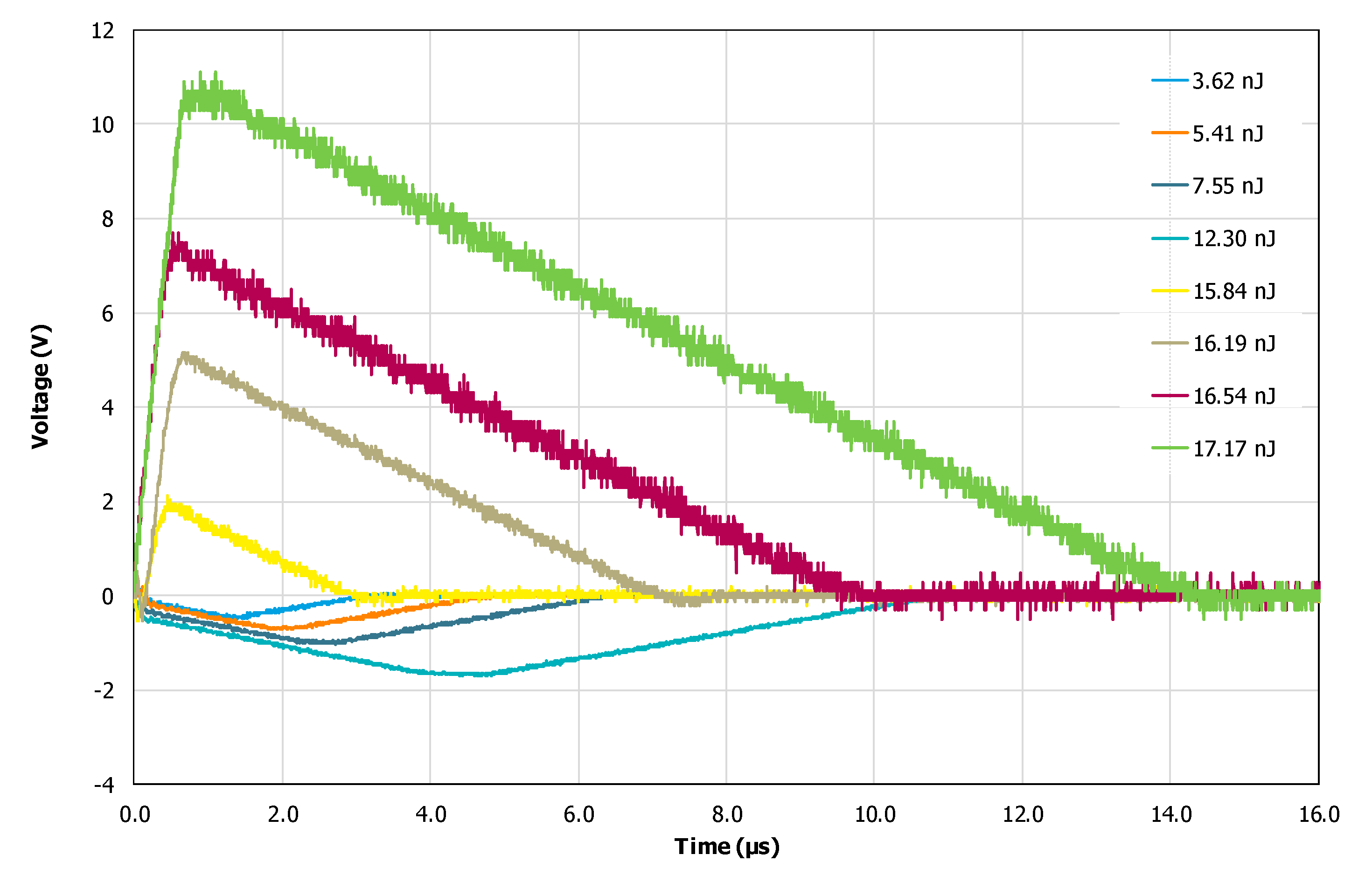
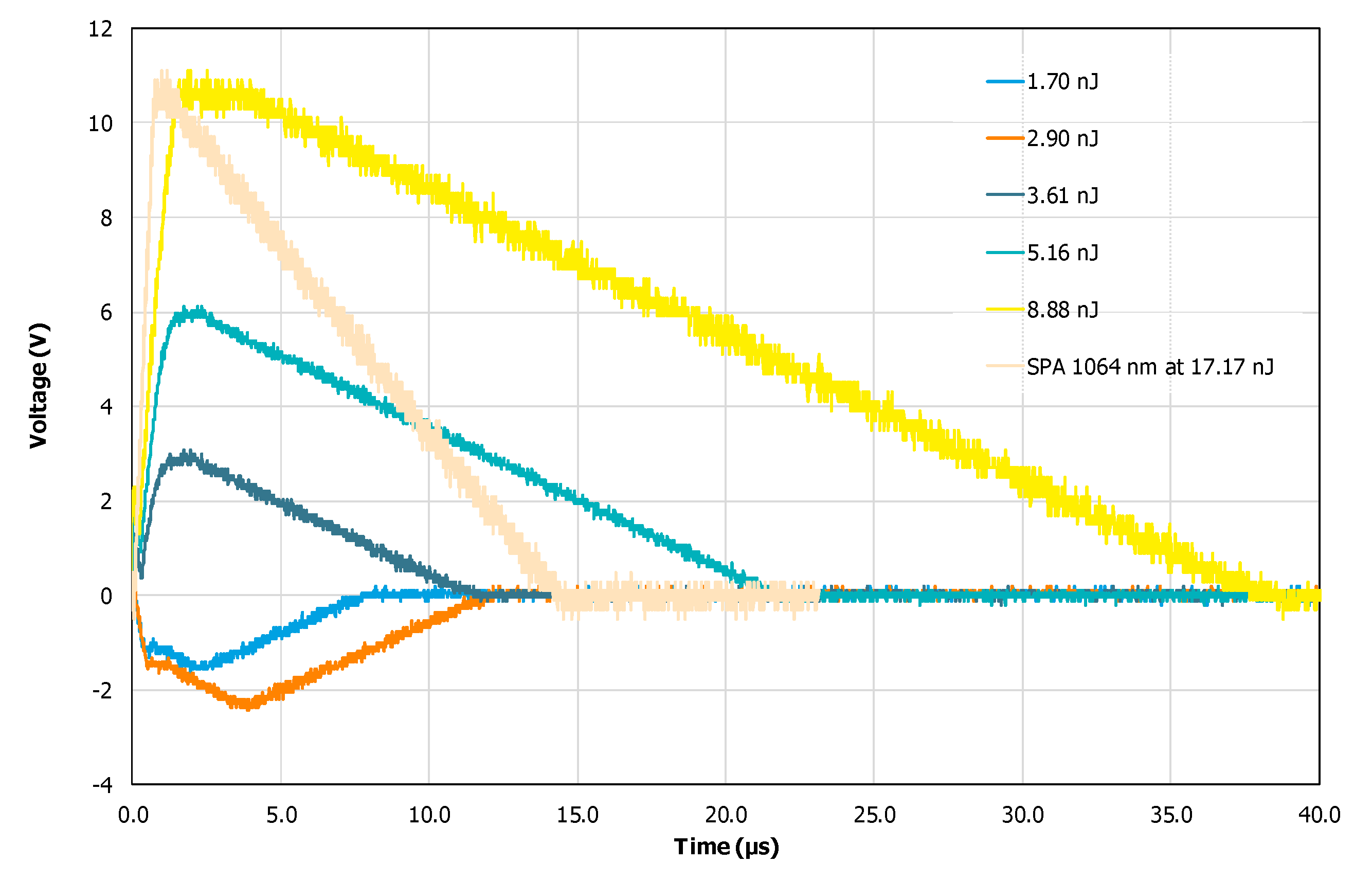
Based on the above measured data, the voltage varies with the laser pulse energy and the focal plane position, as a function. The Y-axis represents the average quantity at each position. Since the laser beam is incident vertically to the surface of the device, the X-axis position is defined as the Z-position, corresponding to the distance traveled along the Z-axis of the DUT. In the data graph, the right side of z = 0 indicates that the focal plane of the laser beam moves in the internal direction of the DUT.
3.3. Test Setup
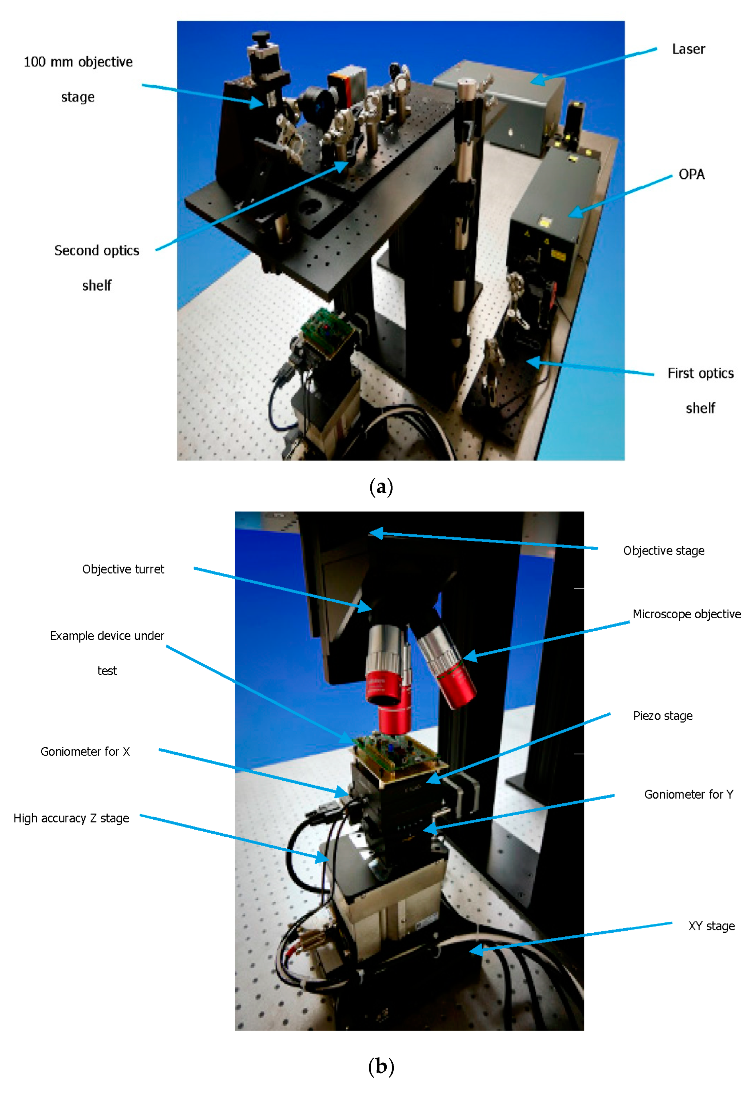
The pulse width of the pulse laser used in the test was 120 fs, the diameter of the focal spot was 1.5 μm, and the repetition rate of the pulse laser was 1 kHz. The pulse laser wavelengths used in the SPA and TPA tests were 1064 nm and 1260 nm, respectively. The test equipment is shown in
Figure 4, below.
The X- and Y-axis loaders represent long distances in the X and Y directions and are commonly used for the initial alignment of the device under test, automatic leveling, and laser scanning equipment.
5. Conclusions
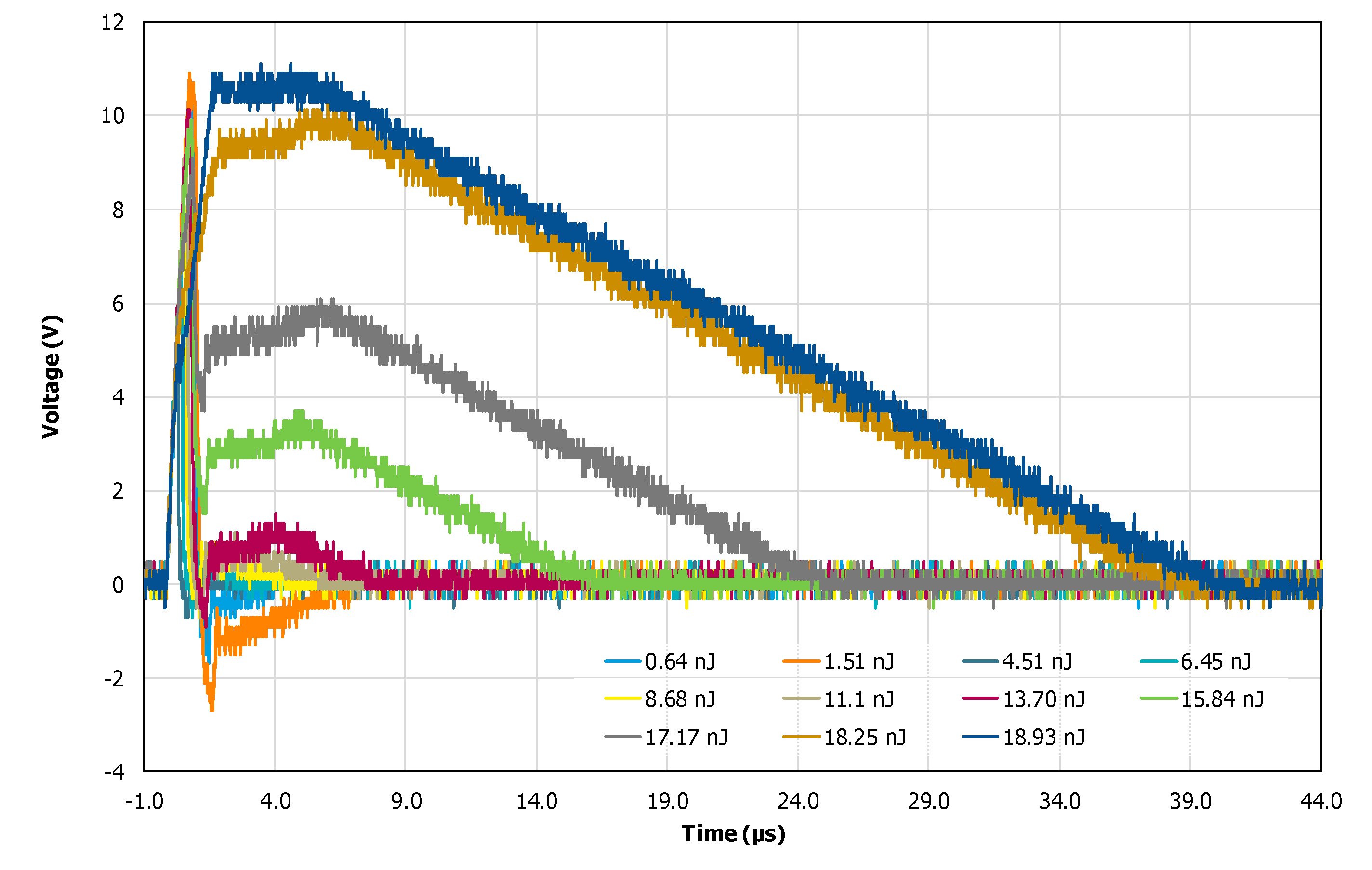
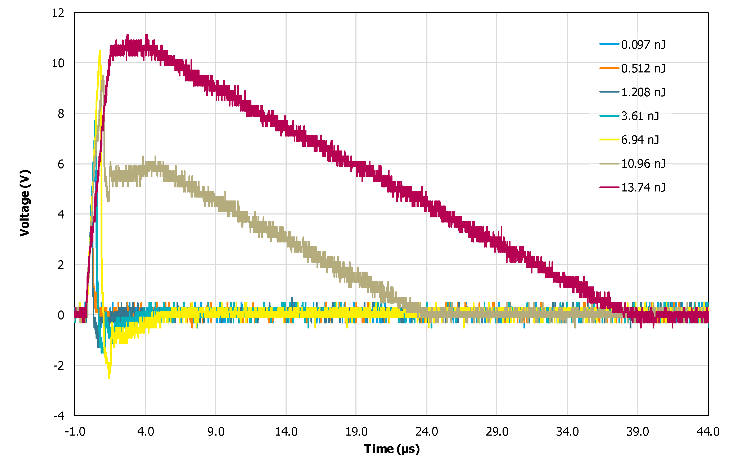
Based on the two-photon absorption-produced and carrier-femtosecond-pulsed-laser-induced effects of single-event simulation test technology, we can see that the single-event effect of the pulse laser micro-nano electronic device simulation test is valuable in a specific sense: partly due to the reduced device process size, the integration can be enhanced, and the rate of the device can be made faster at the same time. The other way in which this test is valuable is related to the unique properties of the TPA process when the pulsed laser passes through the wafer, which means that the laser is injected directly into the specified location of the complex circuit, avoiding the influence of the metal layer’s interface. This test method can enable the formation of meaningful qualitative judgments and insights relating to, for example: radiation-sensitive node identification; the reinforcement of the circuit design; the mechanisms of the validation and calibration of basic research models; space missions with the screening of electronic components and their injection in complex circuit fault to analyze error propagation characteristics, etc., which can, in electronics, resist radiation evaluation; reinforcement design verification provided in space-time; and other important information about the effects of a single event. In this study, the differences between the SPA- and TPA-induced single-event transient effects were compared based on the single-event transient effects of typical operational amplifiers. According to the results, it can be seen that the transient voltage slope slopes induced by SPA and TPA were basically the same. The energy of the SPA test with 1064 nm light was about half of the energy of the TPA test with 1260 nm light. Moreover, it can be seen from the results that, when the pulse laser energy was low, the transient voltage firstly appeared as a positive polarity pulse, and with the increasing pulse laser energy, the transient voltage pulse presented as a positive pulse with a larger amplitude. This may be related to the amount of the deposited charge. As the pulse energy increased, more charges were deposited.
These experimental results show that the TPA SEE test technique is an effective means of testing the single-event effect of a pulsed laser in high-frequency, high-speed, and high-integration devices, which can be used in the future. Meanwhile, the Z-scanning technology of TPA SEE can use a single wavelength laser to determine the depth of the sensitive volume of the device, which has positive practical value for the device performance evaluation and anti-radiation reinforcement design.


