Review

Recent Advances in the Growth and Characterizations of SILAR-Deposited Thin Films

Faculty of Health and Life Sciences, INTI International University, Putra Nilai 71800, Negeri Sembilan, Malaysia
Appl. Sci. 2022, 12(16), 8184; https://doi.org/10.3390/app12168184
Submission received: 2 July 2022 / Revised: 29 July 2022 / Accepted: 2 August 2022 / Published: 16 August 2022
(This article belongs to the Section Materials Science and Engineering)

Abstract

:
Many researchers have reported on the preparation and characterization of thin films. The prepared thin films could be used in lasers, cathodic ray tubes, solar cells, infrared windows, ultraviolet light emitting diodes, sensors, supercapacitors, biologic applications, and optoelectronic applications. The properties of these thin films strongly depend on the deposition techniques. Throughout the years, many investigations into the production of various types of thin films (by using the successive ionic layer adsorption and reaction (SILAR) method) were conducted. This method attracts interest as it possesses many advantages when compared to other deposition methods. For example, large area depositions could be carried out in any substrates at lower temperatures via inexpensive instruments; moreover, a vacuum chamber is not required, it has an excellent growth rate, and the unique film properties could be controlled. In this work, metal sulfide, metal selenide, metal oxide, and metal telluride were deposited on substrates by using the SILAR method. According to the findings, both thick and thin films could be synthesized under specific conditions during the experiment. Additionally, the results showed that the number of deposition cycles, rinsing times, immersion times, and concentrations of the precursors affected the crystallinities, grain sizes, film thicknesses, surface roughness, and shapes of the obtained films. These films could be used in solar cell applications with high power conversion efficiency due to the appropriate band gap value and high absorption coefficient value.

1. Introduction

Thin films have attracted much interest because they possess unique properties [1]. Several physical methods and chemical deposition techniques were used for the growth of thin films on substrates. These deposition methods include electrodeposition [2], chemical bath deposition [3], magnetron sputtering, chemical vapor deposition, spray pyrolysis, thermal evaporation [4], molecular beam epitaxy, ion beam deposition, electron beam evaporation, atomic layer epitaxy, the spin coating method [5], the pulsed laser deposition method, and the successive ionic layer adsorption and reaction (SILAR) technique. The advantages and disadvantages of these deposition techniques are highlighted as shown in Table 1. The prepared thin films could be used in lasers, cathodic ray tubes, solar cells [6], infrared windows, ultraviolet light-emitting diodes, sensors [7], supercapacitors, and biologic and optoelectronic applications [8].
The advantages of the SILAR method, including a large area deposition, could be carried out in any substrate at lower temperatures by using simple techniques and inexpensive instruments [9]; stoichiometry, thickness, morphology, and grain size could be controlled [10]; there are material and production cost savings [11]; a vacuum chamber is not required; there is excellent growth rate and non-formation of precipitate in the container. Generally, the SILAR deposition technique background could be represented by the adsorption and reaction of ions (anions and cations from solutions) and the rinsing process (deionized water) to prevent precipitation in the solution. The SILAR technique consists of four steps [12], namely adsorption (the cation is adsorbed on the substrate surface), the first rinsing with water (the excess adsorbed ions are rinsed away), the reaction process (introducing the anionic ion into the system), and the second rinsing (the unreacted species and excess ions are removed). The formation of thin films on the substrate could be observed by repeating these cycles [13]. The complexing agents, rinse times, immersion times, deposition cycles, concentrations of the precursor solutions, and the nature of the precursors were shown to affect the SILAR growth phenomena. In this work, specific terms, such as “ionic product” and “solubility concept” will be discussed briefly to help the reader understand the SILAR deposition technique. When the sparingly soluble salt (EF) was reacted with water, the saturated solution consisted of the A+ ion and B- ion, as indicated in the following equation:
EF s E + + F
K = C E + · C F / C EF
K K = C E + · C F
K s = C E + · C F
Here, the concentrations of E+, F, and EF are represented as C E + , C F , and CEF, respectively. Generally, the concentration of pure solid was considered a constant number (K′). We knew that K and K′ were so-called constant values. The product of KK′ was identified as a constant value as well and could be labeled as Ks. In the SILAR deposition method, Ks and C E + , C F are called the solubility product and ionic product, respectively. We can observe that the ionic product is equal to the solubility product in the saturated solution, In the supersaturated solution, precipitation occurs, and ions combine to produce nuclei when the ionic product is more than the solubility product.
In this work, we will describe the preparation of metal sulfide, metal oxide, metal telluride, and metal selenide thin films by using the SILAR deposition technique. The thin film growth and reaction mechanisms will be highlighted based on the literature. The properties and applications of the obtained nanostructured thin films will be discussed.

2. Metal Sulfide Thin Films

Sulfur is non-metallic, abundant, and has an atomic number of “16” with the symbol “S”. Generally, sulfur is very low in toxicity (to humans) as our bodies require it for certain activities.

2.1. Silver Sulfide Films

Nanostructured n-type silver (I) sulfide (Ag2S) films were deposited onto fluorine-doped tin oxide (FTO)-coated glass [14]. Photoelectrochemical studies revealed that high series resistance caused a very low value of power conversion efficiency. Nanoscale highly-conducting Ag2S films with thicknesses of 299 nm were produced under specific conditions, such as immersion time = 25 s, deposition cycle = 50 cycles, and rinse time = 15 s [15]. The obtained films were homogeneous and polycrystalline with the most intense peaks along (100) the planes based on the field emission sacking electron microscopy (FESEM) and the X-ray diffraction (XRD) analysis. The energy dispersive X-ray analysis (EDX) spectra confirmed silver richer in these films. The films (thickness = 0.22 µm) were synthesized onto amorphous glass at 27 °C by using thiourea (SC(NH2)2) and silver (I) nitrate (AgNO3), which were annealed under various temperatures. The XRD data supported the recrystallization process, causing bigger grain sizes at higher annealing temperatures. Electrical resistivity (2.58 to 1.99 × 10⁴ Ω·cm) and the band gap (1.07 eV to 1 eV) were reduced with increasing temperatures (from 373 to 573 K) [16]. The deposition of Ag2S (silver sulfide) films took place on glass slides by using a complexing agent (ammonia (NH3)) at 40 °C [17]. Films showed monoclinic phases and preferred orientations corresponding to the (120) plane. Improvements in crystallinity and the red shift in absorption edge could be observed when the deposition cycle increased from 20 to 50 cycles. Thiourea and silver nitrate were used to produce thin films under 30 deposition cycles, at 27 °C; the rinse time was 10 s, and the immersion time was 15 s [18]. The film thickness and crystallite size were 135 and 21.38 nm, respectively. In the optical studies, the absorption edge was observed at 620 nm, showing a band gap of 2.09 eV. Other researchers have highlighted that these films could be used in sensitized solar cells due to the non-toxic materials [19], excellent short circuit currents, and compatibility with the polysulfide electrolyte [20].

2.2. Copper Zinc Tin Sulfide Films

The copper zinc tin sulfide (CZTS) uniform films were prepared at room temperature on glass substrates [21]. The resistivity value, band gap, mobility, absorption coefficients, and carrier density were 1.51 × 10² Ω·cm, 1.5 eV, 0.32 cm2V−1⋅s−1, 104 cm−1, and 1.28 × 1017 cm−3, respectively. Based on the Raman spectroscopy and XRD studies, two peaks (287 and 336 cm−1) could be observed and the films showed tetragonal phases, respectively [22]. Gayatri and co-workers [23] reported that the grain sizes increased with the increasing deposition cycles during the experiment. The scanning electron microscopy (SEM) results revealed the formation of porous grains in the obtained samples. Low-cost non-toxic CZTS films were produced on fluorine-doped tin oxide (FTO) glass by Sawanta and co-workers [24]. Photovoltaic behaviors (Voc = 390 mV, Jsc = 636.9 µA/cm2, fill factor = 0.62, power conversion efficiency = 0.396%) in a photoelectrochemical solar cell were reported. On the other hand, Suryawanshi and co-workers [25] studied the influence of anionic bath immersion time on the photovoltaic characteristics. The best results were obtained for shorter immersion times (power conversion efficiency = 2.33%, short circuit current (Jsc) = 12.88 mA/cm2, open circuit voltage (Voc) = 0.42 V, fill factor = 0.43).

2.3. Tin Sulfide Films

The n-type tin (IV) sulfide or tin disulfide (SnS2) films were synthesized onto various types of substrates. The XRD confirmed that the nanocrystalline grain growth and amorphous structure could be detected in silicon (Si) (111) substrate and glass substrate, respectively. The band gap was 2.6 eV while electrical resistivity was 103 Ω·cm [26]. The triethanolamine (TEA) was used to produce tin (II) sulfide (SnS) films onto glass substrates. It was very clear that the band gap value reduced when the particle size and molar concentration of TEA increased during the experiment [27]. The SnS films were synthesized by using tin (II) chloride or stannous chloride (SnCl2) and ammonium sulfide ((NH4)2S) [28]. The Fourier transform infrared spectroscopy (FTIR) studies revealed that several peaks (602.48 cm−1, 1094.78 cm−1, 1380.64 cm−1, 1630.76 cm−1, and 2364.41 cm−1) could be observed because of the unique characteristics of the films. The nanostructured SnS films (thickness = 0.2 µm) were produced onto indium tin oxide-coated glass (ITO) substrate by using Na2S (sodium sulfide) and SnSO4 (tin (II) sulfate or stannous sulfate) solutions [29]. The obtained films showed high absorption in the visible area (ultraviolet (UV)-visible transmission spectrum), were rich in tin elements (EDX studies), and indicated sharp peaks at 680 and 825 nm (photoluminescence spectrum). There was growth of thin films (Equation (1)) by using SnCl2 and Na2S under 40 deposition cycles, as reported by Qachaou and co-workers [30]. As highlighted in the XRD studies, the lattice parameters were a = 4.07 Å, b = 4.13 Å, and c = 11.45 Å, respectively. Raman spectroscopy indicated the SnS phase without any secondary phase.
SnCl 2 + Na 2 S SnS + 2 NaCl  
The complexing agent (ethylene diamine tetra acetic acid (EDTA)) was employed during the formation of SnS films at room temperature [31] by using a tin (II) nitrate (Sn(NO3)2) solution and Na2S solution, as indicated in Figure 1. The band gap reduced (2.31 to 2.09 eV) when the molar concentration of EDTA increased from 0.05 to 0.2 M.

2.4. Copper Tin Sulfide Films

The XRD studies confirmed that the orthorhombic phase of Cu4SnS4 (CTS) and the cubic phase of Cu2SnS3 could be prepared under hydrogen sulfide (H2S) atmosphere and nitrogen and sulfur vapor mixture conditions, respectively. The activation energies were 0.1 eV and 0.06 eV in Cu2SnS3 and Cu4SnS4 films, respectively [32]. The n-type Cu2SnS3 films were prepared on stainless steel in the presence of ethylene diamine tetra acetic acid disodium (Na2EDTA), as reported by Harshad and co-workers [33] and indicated in Figure 2. The sodium sulfide was used as anionic while copper (II) chloride (CuCl2) and tin chloride (SnCl2) acted as cationic precursors. The proposed reaction mechanisms are highlighted in Equations (2)–(5). During the formation of thin films, the substrate was immersed in a cationic solution and anionic solution and then rinsed with double distilled water (DDW) to prevent precipitation (Figure 2).
2 CuCl 2   + SnCl 2 2 Cu + + 6 Cl + Sn 4 +
Na 2 S + H 2 O OH + HS + 2 Na +  
HS + H 2 O S 2 + H 3 O +
2 Cu + + Sn 4 + + 3 S 2 Cu 2 SnS 3
The X-ray photoelectron spectroscopy (XPS) studies highlighted the +1 and +4 in copper and tin, respectively. The XRD and SEM studies showed that the triclinic phase and spherical grains covered the entire surface of the films, respectively. Brunauer–Emmett–Teller and wettability investigations confirmed the mesoporous with the surface area (2.1 m2/g) and hydrophilic nature of the obtained films. The surface area is one of the very important parameters used to study light absorption in various incident angles. Cu2SnS3 films were annealed at 350 °C under 60 min in the sulfur (S) atmosphere [34]. The XRD studies confirmed the amorphous and polycrystalline in the as-deposited and annealed films, respectively. Optical absorption and EDX investigations showed a smaller band gap (1.21 eV) and excess copper (Cu) concentration in the annealed films. The Cu2SnS3 films were deposited onto an indium-doped tin oxide glass substrate, showing uniform morphology and a blackish color [35]. The annealed films (300 °C in vacuum) indicated higher intensities when compared to as-deposited films based on the XRD studies. The X-ray photoelectron spectroscopy (XPS) confirmed Cu1+, Sn4+, and S2− in the obtained films. The highest power conversion efficiency (0.11%) and fill factor (30%) were achieved in ITO/CTS/lithium perchlorate/graphite solar cells. The high phase purity of Cu2SnS3 could be deposited onto a soda lime glass substrate [36]. The absorption coefficient was 104 cm−1 and reflectivity was 10% at 200–600 nm. Cu5Sn2S7 and Cu3SnS4 films were prepared onto a glass substrate at a specific speed (400 nm per 60 min) [37]. Researcher findings showed excellent conductivity, a higher absorption coefficient (more than 104 cm−1), and strong optical absorption in the near-infrared reflectance (NIR) region. The band gap values were 1.45 and 1.47 eV in Cu5Sn2S7 and Cu3SnS4, respectively.

2.5. Zinc Sulfide Films

Zinc acetate or acetic acid, zinc(II) salt (Zn(CH3CO2)2), and sodium sulfide solution were used to produce ZnS films onto the glass substrate [38]; the growth mechanisms are explained in Equations (6)–(9).
Zn ( CH 3 COO ) 2 Zn 2 + + 2 CH 3 COO
Na 2 S + H 2 O Na + + SH
OH + SH H 2 O + S 2
Zn 2 + + S 2 ZnS
The formations of ZnS films were reported by using zinc acetate, thiourea, and a complexing agent (ammonium hydroxide, (NH4OH)). Based on the photoluminescence studies, three sharp peaks (413, 480, and 525 nm) could be detected. Further, the reduction of the intensity due to the concentration of sulfur increased [39]. The deposition of thin films onto fluorine-doped tin oxide glass was reported by Mana and co-workers [40]. The band gap reduced from 3.62 to 3.5 eV when increasing the deposition cycle (40 to 70 cycles). The FESEM analysis revealed a mesoporous nature and a thickness of 1.43 µm. Photovoltaic parameters were studied by using the photoelectrochemical solar cell. The fill factor, power conversion efficiency, open circuit voltage (Voc), and short circuit current (Jsc) were 0.59, 0.1%, 0.52 V, and 0.35 mA/cm2, respectively, when the films were prepared under 70 deposition cycles. Zinc (II) chloride (ZnCl2), triethanolamine, and sodium sulfide solutions were used to produce films [41]. The XRD studies confirmed that the amorphous phase changed to the crystalline phase as the deposition temperature increased. Ammonia was used as a complexing agent during the preparation of films [42]. The obtained films showed a crystallite size of about 12 nm with a thickness of 1 µm. The activation energy was 0.6 eV, and an increase in temperature caused a decrease in electrical resistance. Laukaitis and co-workers [43] reported that the growth rate of films deposited on a gallium arsenide (GaAs) substrate was 0.23 nm per cycle. The XRD studies revealed that the highest reflection could be seen at 2θ = 29°, contributing to the (111) plane in the films (film thickness = 136 nm). Experimental findings showed the highest tensile stress (6.9 × 10⁸ N/m2) for the obtained films (surface roughness = 2.9 nm, thickness = 50 nm). The soda–lime glass was used to produce films [44] by using TEA under the immersion time (20 s). The refractive indices and growth rates were 1.95–2.23 and 0.13–0.27 nm/cycle, respectively. To our knowledge, there was only one publication published on zinc sulfide thin films, produced by using two deposition techniques (the SILAR method and thermal evaporation technique). This comparison was very unique (Table 2); the properties of the obtained thin films were studied for the first time.

2.6. Lanthanum Sulfide Films

Preparation of lanthanum sulfide films took place on a stainless steel substrate by using lanthanum (III) chloride (LaCl3) and Na2S solution [45]. Several phases, such as the tetragonal (2θ = 28.7°) and monoclinic structure (2θ = 20.7° and 31.1°), could be detected based on the XRD patterns. The crystallite size was 1.4 nm in each sample. FESEM micrographs showed sponge-like porous morphology with grain sizes smaller than 0.5 µm. Other experimental results, including a small semicircle arc, were observed in the middle-frequency region; the contact angle was 47.6°.

2.7. Copper Sulfide Films

The copper sulfide (CuS) films were deposited onto various substrates (glass and Si(111) wafer) by using a thiourea and copper (II) sulfate (CuSO4) solution [46]. Highly polycrystalline films were produced by using a Na2S and CuSO4 solution. The obtained films showed uniform morphology with the covellite phase and could be used for optoelectronic device applications [47]. The cupric sulfate (CuSO4) and sodium thiosulfate (Na2S2O3) were employed to form CuS films at room temperature. A significant change in the surface morphology of the films could be observed at 100 cycles (irregular microspheres), 150 cycles (bigger in size), and 200 cycles (flower-like agglomerated grains). Overall results indicated a high absorbance value in the visible range, excellent optical features, and a direct band gap value (1.95 eV to 1.98 eV). The growth of CuS films under normal pressure was studied. The researchers pointed out that the films were rough and the growth rate was proportional to the copper concentration [48]. The influences of the molar concentration on the films were investigated. The band gap dropped (2.26 to 1.86 eV) when increasing the molar concentration (0.05 to 0.25 M). The average transmittance observed was more than 70% of the UV-visible-NIR regions in all films, indicating excellent materials for the optical coatings [49]. The Cu2S films were produced [50] by using different complexing agents, such as a hexamethylenetetramine ((CH2)6N4) and ammonia solution (rinse time was 30 s, immersion time was 20 s, deposition cycles = 100 cycles). The copper sulfate provided cationic ions reacted with the ammonia solution to prepare Cu(OH)2 (solution became turbid) as indicated in equation 10. Then, the complex ion [Cu(NH3 ) 4 2 + ] was produced (solution became clear) by adding the excess ammonia solution as highlighted in Equation (11). Here, the most stable coordination number should be 4. Based on the experiment, a similar type of reaction occurred by using hexamethylenetetramine (Equation (12)). The dissociation of thiourea in the basic conditions (provide S2− ions) and the formation of divalent sulfide ions are represented in Equations (13) and (14), respectively. Lastly, the formations of Cu2S films (a few nanometers) were found in the substrates.
CuSO 4 + 2 NH 4 OH Cu OH 2 + 2 NH 4 + + SO 4 2
Cu OH 2 + 4 NH 4 + 2 H + + 2 H 2 O + [ Cu ( NH 3 ) 4 ] 2 +
( CH 2 ) 6 N 4 + 6 H 2 O 6 HCHO + 4 NH 3
CSNH 2 NH 2 + OH H 2 O + HS + CH 2 N 2
HS 2 + OH H 2 O + S 2
[ Cu ( NH 3 ) 4 ] 2 + + S 2 Cu 2 S + 4 NH 3
Raman spectra and XPS studies showed very strong bands at 472 cm−1 and no other impurities in these samples. The maximum specific capacitance, specific energy, and specific power for the films prepared by using ammonia were 765 F/g, 25.1 Wh/kg, and 12.2 kW/kg, respectively. In this work, thin films produced by using ammonia had better stability over the 2000 cycles when compared to hexamethylenetetramine (93%), based on the high-resolution transmission electron microscopy (HRTEM) results, a thicker structure (d-spacing value = 3.012 Å), and a nanotube structure (d-spacing value = 3.105 Å) by using ammonia and hexamethylenetetramine, respectively.

2.8. Cadmium Sulfide Films

The depositions of CdS films took place on glass slides by using Na2S and cadmium (II) chloride (CdCl2). The immersion and rinsing times were 20 and 40 s, respectively [51]. The obtained films showed very high transmittance (visible region) and stoichiometric compositions. On the other hand, another precursor, such as cadmium acetate (Cd(CH3CO2)2), was used to produce thin films (Equations (16)–(21)).
Na 2 S + H 2 O 2 Na + + SH + OH  
SH + OH S 2 + H 2 O
Cd 2 + + 2 OH Cd OH 2  
Cd OH 2 + 4 NH 2 OH [ Cd ( NH 3 ) 4 ] 2 +  
[ Cd ( NH 3 ) 4 ] 2 + Cd 2 + + 4 NH 3  
Cd 2 + + S 2 CdS
The as-deposited and annealed films (250 °C, under air, 30 min) showed an amorphous phase and polycrystalline nature with the hexagonal structure [52]. The glass substrate was modified by using 3-mercaptopropyltrimethoxysilane to produce good-quality films [53]. The results showed that a faster deposition rate could be observed in the modified substrates. Cadmium chloride and thiourea were used to produce thin films at 80 °C under different deposition cycles [54]. The results of the XRD studies confirmed that the crystallite sizes (12.44 to 14.65 nm) and absorbance edge (525 to 555 nm) increased with increasing the deposition cycles (20, 30, and 40 cycles). Cd(II) organic salt, such as cadmium 2,4-pentanedionate (C10H14CdO4), was used to produce films on glass sheets [55]. The XRD analysis revealed that these films were polycrystalline in nature with various particle sizes (20–80 nm). Garadkar and co-workers [56] reported that homogeneous nanostructured films could be observed when the deposition cycles reached 125 cycles during the experiment. The research findings also revealed that conductivity increased when the temperature increased and the specific conductance was 10−4 to 10−2 (Ω·cm)−1. Cadmium acetate and ammonium sulfide ((NH4)2S) served as cationic and anionic precursors, respectively, during the formation of the films at room temperature [57]. TEM and EDX studies confirmed the average particle size was 23.5 nm and the existence of cadmium and sulfur elements. FTIR spectra showed several peaks in Figure 3, such as 653.37 cm−1 (CdS stretching frequency), 1068.76 cm−1 ( SO 4   traces ), 1408.43 cm−1 (S=O), and 1598.51 cm−1 (C-C stretching vibration).

2.9. Copper Aluminum Sulfide Films

The CuAl2S nanostructured films were produced on a clean glass substrate by using copper sulfate, aluminum sulfate (Al2(SO4)3), thiourea, and ammonia (complexing agents) for 20 deposition cycles, under pH 5.3 [58]. The film thicknesses in the annealed films (100 to 250 °C, 60–120 min) were 100.43 to 135.87 nm. The XRD studies confirmed the monoclinic phase with the sharp peak corresponding to the (101) plane. The SEM analysis indicated a rough surface (with tiny white spots) because of the aluminum ion. These materials could be used in optoelectronic applications as they were linearly reduced in the reflectance value when the wavelength increased from the visible to the near-infrared region.

2.10. Nickel-Doped Indium Sulfide Films

The In2S3Ni films were deposited onto indium tin oxide (ITO)-coated glass by using indium (III) acetate (In(C2H3O2)3), nickel (II) chloride (NiCl2), and sodium thiosulfate under 75 deposition cycles [59]. The sulfur/(In+Ni) ratio (0.79 to 0.4), band gap (1.99 to 1.61 eV), and crystallinity of the sample reduced with the increasing nickel (Ni) concentration (4% to 6%).

2.11. Indium Sulfide Films

The n-In2S3 films were produced by using different precursors, namely indium (III) chloride (InCl3) and indium (III) nitrate (In(NO3)3). Generally, these films were orange and turned red during the annealing process. The films prepared by using In(NO3)3 showed uniform morphology and strong diffraction peaks along the (440) plane. The XRD data supported the films produced by using InCl3, were crystalline (as heated at 400 °C), and exhibited excellent photo responses [60]. The depositions of films took place on amorphous glass substrates, by using indium (III) sulfate (In2(SO4)3), sodium sulfide, and complexing agents (TEA and hydrazine hydrate). The obtained films were very smooth and the band gap value was 2.7 eV [61]. Ranjith and co-workers [62] proposed that thin films were synthesized under different rinsing and dipping times. Bigger grain sizes could be detected in longer dipping times. Jingjing and co-workers [63] reported that these films could be employed for solar energy conversion for several reasons, e.g., low toxicity with good stability, excellent carrier mobility, and excellent photo-absorption coefficients.

2.12. Cobalt Sulfide Films

The p-type CoS films were deposited onto different substrates (glass and single crystal Si (111) wafers) by using a cobalt (II) sulfate (CoSO4) and sodium sulfide (Na2S) solution [64]. The XRD studies revealed the amorphous phase and polycrystalline structure in the glass and silicon (111) wafers, respectively. Steel was used as a substrate during the deposition of films [65]. The optical conductivity and band gap were 1.77 × 10¹⁷ S−1 and 1.9 eV, respectively. The XRD analysis confirmed the hexagonal structure with a crystallize size of about 27.5 nm. The cobalt sulfide films could be used in optoelectronic and energy storage applications due to some unique properties. These films indicated 80% charge capacity retention (even after 1000 deposition cycles) and showed a specific capacity (298.4 mAh/g) at 30 deposition cycles when the scan rate was 20 mV⋅s. Mitkari and co-workers [66] highlighted that the grayish-black color changed to dark black with increasing the deposition cycle (35 to 115 cycles) during the experiment. Further, they explained that films were peeled off from the substrate after 95 deposition cycles. Lastly, they observed that activation energy decreased (0.18 to 0.15 eV) when film thickness increased (201 to 513 nm).

2.13. Nickel Sulfide Films

Preparation of p-type NiS films took place on a single crystal Si (111) wafer [67]. The band gap and the activation energy values were measured to be 0.45 and 0.15 eV, respectively. The band gap values of NiS films produced by using thiourea were 3.12, 2.93, and 2.81 eV when the deposition cycles were 4, 6, and 8, respectively [68]. The band gap values of Ni3S4 films were 2.8 and 2.15 eV for 6 and 8 cycles, respectively. The depositions of NiS films took place by using nickel (II) nitrate (Ni(NO3)2) and sodium sulfide at 27 °C, under unstirred conditions [69]. The XRD studies revealed these films were hexagonal phases, with film thicknesses of 350 nm. Two strong peaks (3480 and 1985 cm−1) could be observed in the FTIR spectrum, indicating C-H stretching modes. Based on the optical absorption investigations, the average optical transmittance and reflectance were 0.62% and 1.1%, respectively.

2.14. Arsenic Sulfide Films

Arsenic sulfide thin films were prepared by using various deposition methods. The obtained films could be used in optical mass memories, hologram recordings, and optoelectronic and solar cell applications. The band gap was 2.6 eV, suitable to be used as an absorber component in thin film solar cells. As2S3 films (of good quality) were deposited onto various substrates (glass and silicon (111) wafers) by using arsenic trioxide or arsenic (III) oxide (As2O3) and Na2S2O3 solution [70].

2.15. Manganese Sulfide Films

The deposition of MnS films on a glass slide was reported by Yildirim and co-workers [71]. The XRD patterns confirmed the polycrystalline phase and SEM images indicated that grains well-covered well the surfaces of the substrates. The band gap (3.39 eV to 2.92 eV) and resistivity (11.84 × 10⁶ to 2.21 × 10⁵ Ω·cm) reduced with the film thickness increase (180 to 350 nm). Sodium sulfide and manganese (II) acetate (Mn(CH3CO2)2) were used to produce thin films as reported by Pathan and co-workers [72] in Equations (22)–(24).
Mn ( CH 3 COO ) 2 Mn 2 + + 2 CH 3 COO
Na 2 S 2 Na + + S 2
Mn 2 + + S 2 MnS
The film thickness and water angle contact were 170 nm and 34° (hydrophilic nature). The synthesis of films onto stainless steel substrates was highlighted by Admuthe and co-workers [73]. The band gap and crystallite size were 2.6 eV and 0.26 nm, respectively. Experimental results showed the highest specific capacitance was 632.9 F/g, under 100 mV/s (scan rate), indicating these films could be used in supercapacitor applications.

2.16. Iron Sulfide Films

The SILAR-deposited FeS films were prepared at 0.15 M of the complexing agent (TEA), showing the best nano-crystal structure [74]. The obtained films could be used for solar cell applications due to their excellent transmittance properties and high absorption coefficients (more than 5 × 105 cm−1, wavelength less than 700 nm). In addition, these films showed p-type behaviors and had hole mobilities of about 100 cm2/Vs.

2.17. Copper Indium Disulfide Films

The copper-rich thin films were deposited onto soda lime glass by using CuSO4, InCl3, and CH4N2S solutions. Maheswari and co-workers [75] reported that CuS reacted with In2S3 to produce CuInS2 (CIS) films during the experiment. The depositions of films took place on glass substrates by using InCl3, Na2S, and CuCl2 solutions at room temperature [76]. XPS studies confirmed the stoichiometry of CuInS2. The direct band gap (1.5 eV) and chalcopyrite phase could be observed in the optical absorption spectrum and XRD pattern, respectively. The tetragonal films were prepared as described by Xueqing and co-workers [77]. The photovoltaic parameter, such as the fill factor (0.31), power conversion efficiency (0.92%), Voc (0.35 V), and Jsc (8.49 mA⋅cm−2) were investigated in the CIS-sensitized solar cells. Fanghong and co-workers [78] noted that the annealed films (200 °C, 1.5 h) were slightly sulfur-rich and showed well-crystalized conditions. The influence of the [Cu]/[In] ratio on the physical properties of the annealed films (argon condition, 500 °C, 60 min) was studied by Zhengguo co-workers [79]. They concluded that resistivity and stoichiometry strongly depended on the [Cu]/[In] ratio during the experiment. The glass was used as the substrate during the synthesis of films (by using CuCl2, InCl3, and Na2S) at pH 5, as described by Mutlu and workers [80] in Equations (25)–(27). The immersion and rinsing times were 30 and 50 s, respectively.
CuCl 2 + Na 2 S CuS + 2 NaCl
2 InCl 3 + 3 Na 2 S 6 NaCl + In 2 S 3
2 CuS + In 2 S 3 S + 2 CuInS 2

2.18. Lead Sulfide Films

The PbS films were deposited on soda lime glass in the presence of the TEA solution [81]. SEM and XRD studies showed rough morphology and the strongest diffraction peak corresponding to the (200) plane. The growth of the films could be observed on silicon (100) and silicon (111) substrates at room temperature [82]. The XRD analysis confirmed the cubic phase and polycrystalline (in nature). The microscope glass slide was used as the substrate during the formation of thin films [83]. The thickness and crystalline size were 480 and 18.6 nm, respectively. Other results showed the band gap was 1.77 eV and the films were cubic structure. Guneri and co-workers [84] highlighted that the extinction coefficient, refractive index, and imaginary dielectric constants varied when the immersion cycle increased during the experiment. The XRD studies exhibited the cubic structure, the strongest peak changed from the (111) to the (200) plane with the increasing dipping cycles. The influence of pH on the properties of the films was reported [85]. According to XRD data, with the average crystallite sizes in the range of 16–23 nm, improvement in the crystalline could be observed with increasing the pH value. Room temperature resistivity (1.2 × 10⁷ to 3.5 × 10⁷ Ω·cm) and direct band gap values (0.99 to 1.84 eV) were also concluded. Vishal and co-workers [86] proposed that PbS could be used as a gas sensor. The XPS analysis confirmed the formation of a stoichiometric compound. FESEM showed clearly visible compact grains (Figure 4) for the films deposited by using a 0.25 M precursor concentration when compared to other concentrations. The thickness and grain size were 232.9 and 100 nm, respectively. These films exhibited the highest sensitivities because of the highest rough surface (i.e., the total number of sites for the adsorption of gas was increased).

2.19. Molybdenum Sulfide Films

The molybdenum sulfide (MoS2) is known as transition metal dichalcogenide. This material has very unique properties, such as a tunable band gap value and flexible mechanical behaviors. MoS2 thin films were deposited on various substrates (a glass slide, FTO, and silicon (111) wafer) by using sodium sulfide [87] and ammonium molybdate ((NH4)2MoO4). Research findings show that these films have appropriate band gaps (1.3 eV) and excellent absorption coefficient values (2.8 × 106 cm−1).

2.20. Antimony Sulfide Films

The Sb2S3 films were deposited on glass slides [88]. The XRD and EDX analyses showed the orthorhombic phase and non-stoichiometric films, respectively. The Raman spectroscopy revealed two major peaks (250 and 300 cm−1) in all samples. Photoluminescence spectra indicated broad bands (430–480 nm) with very strong blue emission peaks (460 nm) in all films. Antimony (III) trioxide (Sb2O3) and sodium thiosulfate were used to produce thin films on the glass substrates [89]. It was observed that film thickness increased up to 0.78 µm (14 deposition cycles), then films began to peel from the substrates. The band gap, resistivity value, and activation energy were 1.8 eV, 107 Ω·cm, and 0.14 eV, respectively.

2.21. Bismuth Sulfide Films

The bismuth sulfide (Bi2S3) films were produced in the presence of 2-methoxyethanol (C3H8O2) to control the solubility of Bi3+ ions. The obtained films showed the orthorhombic phase with a band gap of 1.6 eV. The highest photocurrent density reached 1 mA/cm2, indicating good photon-to-electron conversion properties in photoelectrochemical cells [90]. The annealed films (200 °C in argon atmosphere) improved the crystallinity when compared to the as-deposited films (amorphous phase). The films showed high absorption coefficients (more than 104 cm−1) in the visible region [91]. The n-type films were deposited on glass slides at room temperature [92]. The annealing process was carried out at 250 °C, 30 min in the air. SEM studies revealed that grains completely covered the substrate surfaces. Photosensitivity enhancement could be observed in the annealed films, making these materials very useful in sensor applications. Formation of the films could be carried out (70 deposition cycles) by using bismuth (III) nitrate (Bi(NO3)3), TEA, and sodium sulfide on the stainless steel substrate, as suggested by Shrikant and co-workers [93]. Based on the XRD pattern, the strong peaks corresponded to the (111) plane with a crystallite size of about 34 nm. SEM images confirmed that porous nanostructures could provide higher kinetics for electrochemical reactions. Experimental results highlighted interconnected nanoparticles caused good energy density (8.89 Wh/kg at 1.4 Ag−1), high specific capacitance (289 F/g), and high power density (1147 W/kg at 3.2 Ag−1).

2.22. Cobalt Tin Sulfide Films

The formation of CoSnS thin films took place on a soda lime glass slide [94] by using cobalt sulfate, tin chloride, ammonia (complexing agent), and thioacetamide (C2H5NS) (rinsing time = 10 s, immersion times = 20 s). The XRD studies indicated that polycrystalline with the diffraction peaks could be observed in (200), (201), (211), and (221) planes. However, secondary phases, such as hexagonal CoS, orthorhombic Sn2S3, cubic Co9S8, and hexagonal SnS2 could be detected in the XRD patterns also. Optical investigations confirmed that absorption was very high when the wavelength was less than 350 nm; however, absorption was reduced in the visible and near-infrared regions. Based on the findings, the refractive index reduced (3.11 to 2.94), but the band gap (1.22 to 1.52 eV) and electronegativity (1.6928 to 1.7168) increased when increased with increasing the deposition cycles from 40 to 80 cycles.

3. Metal Selenide Thin Films

Selenium has an atomic symbol of “Se” with an atomic number of 34. It could be observed in crooksite and clausthalite. The investigations of selenium have attracted great attention because of selenium-indicated photovoltaic action and photoconductive action.

3.1. Cadmium Selenide Films

The films were produced under various immersion cycles (30, 40, 50, and 60) by using cadmium chloride, sodium selenosulfate (Na2SeSO3), and ethylene diamine tetra acetic acid (EDTA) (complexing agent) [95]. Generally, homogeneous morphology and the hexagonal phase could be seen in all samples. The peak intensity (corresponding to (101) plane) absorbance value increased, but the band gap decreased with the increasing number of immersion cycles. Tartaric acid (C4H6O6) was used as a complexing agent during the formation of thin films at 27 °C under 45 cycles [96]. The reaction mechanisms are highlighted in Equations (28)–(31).
Na 2 SeSO 3 + OH HSe + Na 2 SO 4
OH + HSe H 2 O + Se 2
[ Cd tartaric   acid ] 2 + tartaric   acid + Cd 2 +
Cd 2 + + Se 2 CdSe
The high-resolution transmission electron microscopy (HRTEM) displayed small particle sizes (30–40 Å) while the EDX spectrum showed that the atomic percentage of Cd:Se was 55:45. Resistivity reduced when the temperature increased, indicating the semiconductor nature of the films. The films prepared onto commercial glass slides at room temperature showed a cubic phase, a band gap of 2.1 eV, and electrical resistivity of about 106 Ω·cm [97].

3.2. Bismuth Selenide Films

The growth of bismuth selenide (Bi2Se3) films onto fluorine-doped tin oxide (FTO) glass [98] at 27 °C (Immersion time = 50 s, rinsing time = 30 s, 150 deposition cycles). Experimental results showed n-type semiconductor and film thickness was 0.92 µm. The current voltage (I–V) characteristics for n-Bi2Se3/polysulfide photoelectrochemical cell in the dark (poor rectification) and illumination conditions (moved to the fourth quadrant, indicated photoactive) were described (Figure 5). The conversion efficiency (0.032%) and fill factor were very small values because of low shunt resistance. The single crystalline wafer of Si (111) and glass substrate were used to produce thin films as stated by Lokhande and co-workers [99]. Film thickness was 1.2 µm and presented homogeneous morphology. Bismuth nitrate, sodium selenosulfate, and the TEA (complexing agent) were used to prepare thin films at 300 K, (immersion time was 60 s, rinsing time was 40 s) [100]. The obtained materials could be used in solar energy-related applications.

3.3. Zinc Selenide Films

Zinc acetate and sodium selenosulfate were used to prepare n-type zinc selenide films [101]. EDX and XRD results showed the films were selenium deficient and amorphous phases, respectively. The band gap and electrical resistivity value were 2.8 eV and 107 Ω·cm, respectively. The influence of the number of cycles on the properties of films was studied by Geethanjali and co-workers [102]. Generally, the hexagonal wurtzite phase—the well-defined nano-grain structure—could be seen in all samples, as well as high transmission (more than 80%) in visible and infrared regions. They observed that the film thickness, band gap, and grain size increased, but the microstrain and dislocation density reduced when the deposition cycle increased from 40, 50, to 60 cycles. Guzeldir and co-workers [103] reported on the synthesis of thin film on silicon substrates for 45 deposition cycles. Experimental findings showed good rectifying properties at room temperature in Zinc/ZnSe/n-Silicon/gold-antimony sandwich structures.

3.4. Cobalt Selenide Films

Films were prepared on a soda lime glass by using sodium selenite (Na2SeO3) and cobalt (II) chloride (CoCl2). Based on the FESEM studies, the uniform grain size was observed when the anionic immersion time was 30 s [104]. Optical properties revealed a band gap of about 2.1 eV [105]. The microscope glass slide was employed as the substrate during the preparation of thin films under a rinse time of 10 s, an immersion time of 30 s, and 12 deposition cycles [106]. The XRD studies revealed a cubic phase of Co9Se8, with lattice parameter values are a = b = c = 10.431 Å. The influence of the deposition cycles on the compositional of the films was studied [107]. The atomic percentages for cobalt (Co) and selenium (Se) were 53.52%:46.48%, 27.01%:72.99%, 39.73%:60.27%, under 10, 15, and 20 cycles, respectively. The CoSe2 films were produced by Egwunyenga and co-workers [108] at room temperature. Film thicknesses and crystallite sizes were 92.96 to 225.63 nm and 7.63 to 13.07 nm, respectively. They observed that the extinction coefficient and absorbance value reduced when the wavelength increased.

3.5. Zinc Indium Selenide Films

The nanostructured n-type ZnInSe films were deposited on a glass slide at room temperature by using indium (II) chloride (InCl2), ZnCl2, and Na2SeSO3 solutions. These films were located in the family of the II–III–VI Group. According to the research results, these compounds showed a tetragonal phase, with specific lattice constants (a = 5.7095 Å, b = 11.449 Å) in the I-42m space group. Energy dispersive X-ray fluorescence results confirmed that the obtained films had cation-rich conditions; the sample compositions were 2% zinc, 30% selenium, and 68% indium. Based on the SEM analysis, small spherical grains completely covered the substrate surfaces. The band gap was 2.09 eV, according to the optical absorption investigations [109].

3.6. Copper Indium Diselenide Films

The p-type CuInSe2 films were synthesized onto glass slides in the presence of a complexing agent, such as triethanolamine (TEA) and sodium citrate (CitNa), as indicated in Equations (32) and (33). The obtained films were heated at 400 °C under an argon atmosphere to remove the detrimental secondary phase [110]. Finally, the formation of films could be seen in Equation (34).
Cu TEA 2 + + Se 2 TEA + CuSe
2 In CitNa 3 + + 3 Se 2 2 CitNa + In 2 Se 3
(2CuSe + In2Se3 → Se + 2CuInSe2)
Deposition of films was carried out at 70 °C by using cupric chloride (CuCl2), indium chloride, and Na2SeSO3 solution [111]. Experimental results showed that smooth morphology and well-crystallized structures were observed in the annealed films (in Argon, 400 °C). The formation of CuInSe2 films could be confirmed based on the XPS analysis [112].

3.7. Copper Selenide Films

During the experiment, copper sulfate and Na2SeSO3 solutions were used to provide cationic and anionic, respectively [113]. The formation of thin films took place on a glass slide at room temperature by using tartaric acid under 60 deposition cycles. Film thickness (130 nm) and deposition rate (2.17 nm/cycle) were studied by using the gravimetric method. The greenish brown and reddish brown colors could be observed in the as-deposited and annealed films (573 K, 60 min, nitrogen atmosphere), respectively. The XRD results showed the tetragonal phase (Cu3Se2); the lattice parameters (a = 6.41 Å, b = 4.294 Å) were reported. The atomic percentages of Cu:Se were 55.23:44.77 and 61.31:38.69 in as-deposited and annealed films, respectively, based on the EDX technique. The Raman spectroscopy showed the sharpest peak at 260 cm−1 in both samples (Figure 6). There was a lower band gap (2.15 eV) in the annealed films due to the phase conversion during the formation of films. Algimantas and co-workers [114] reported on the preparation of Cu0.87Se films on glass slides. The visual observation showed the colors of the obtained films were transparent and then changed to dark gray. The XRD studies showed hexagonal klockmannite phases with four diffraction peaks (2θ = 26.6, 28.1, 31.2, and 50°). The XPS spectrum exhibited binding energy around 932.2–932.4 eV (Cu2p3/2), contributing to the CuSe and Cu2Se phases. The atomic absorption spectroscopy (AAS) analysis showed copper-rich films when the temperature increased (from 40 to 60 °C) during the experiment. Betul and co-workers [115] proposed that the obtained SILAR-deposited Cu3Se2 films were polycrystalline in nature, with uniform morphology (without any pores).

3.8. Lead Selenide Films

The deposition of lead selenide films took place on various substrates (glass and ITO glass) by using lead (II) acetate (Pb(CH3CO2)2), triethanolamine, and sodium selenosulfate, at room temperature and under normal pressure [116]. The obtained films were adherent and metallic. The influence of hydrazine hydrate (H6N2O) on the properties of films was reported [117]. Experimental results showed that the highest crystallinity and maximum conductivity could be observed for the films prepared by using 5 mL of hydrazine hydrate. The band gap, average crystallize size, and roughness were 1.425–1.803 eV, 18.18–33.37 nm, 13.7–76.3 nm, in all samples.

3.9. Dysprosium Selenide Films

Dysprosium selenide (Dy2Se3) thin films were deposited onto glass substrates [118]. These materials could be used for electrochemical energy storage. Experimental findings showed the specific capacitance was 92 F/g, when the current density was 2.85 A/g (1M lithium perchlorate (LiClO4) electrolyte), and successfully retained 85% over 5000 cycles, as indicated in the galvanostatic charge–discharge technique. On the other hand, specific capacitance (83 F/g) and specific energy (18 Wh/kg) at specific power (2.7 kW/kg) were highlighted in the Dy2Se3/LiClO4− polyvinyl alcohol (PVA)/manganese dioxide or manganese (IV) oxide (MnO2) flexible hybrid electrochemical capacitor. Lastly, they concluded that this device successfully retained 92% when the ending angle was 160°. Bagwade and co-workers [119] reported on the preparation of thin films onto stainless steel substrates. Orthorhombic phase and spherical grains could be observed based on the XRD and SEM analyses. The obtained films showed specific surface areas of about 48 m2/g and hydrophilic nature (with a contact angle of 50°). Experimental findings confirmed excellent specific capacitance (273 F/g) when the scan rate was 5 mV/s and a 1 M sodium sulfate (Na2SO4) electrolyte.

3.10. Indium Selenide Films

The indium selenide (InSe) films were deposited onto glass substrates (75 cycles) and gallium selenide (GaSe) single crystal substrates (50 cycles), respectively, by using indium (III) sulfate (In2(SO4)3) and Na2SeSO3 solution [120]. The XRD studies revealed the hexagonal phase and lattice parameters, such as a = 7.128 Å, c = 19.382 Å, z = 6 for the films grown on glass. There were two diffraction peaks corresponding to (002) and (004) planes, and the space group was P63/mmc, which could be seen when the substrate was the GaSe single crystal. Other results, such as smaller average particle sizes (26.5–60.2 nm) and absorption maxima, were 2 eV for the films produced by using the glass substrate.

3.11. Boron-Doped Indium Selenide Films

The boron-doped indium selenide (InSe) films were deposited on different substrates [120]. The XRD analysis showed a broad bump because of the glass substrate, and the intensities of the peaks reduced with the boron addition. The absorption tail began from 1.13 eV and ended at 1.96 eV, while Urbach energy was 792 meV when the substrate was on the glass slide.

3.12. Antimony Selenide Films

The Sb2Se3 thin films were deposited on glass substrates by using antimony potassium tartrate (K2Sb2(C4H2O6)2), tartaric acid (complexing agent), and sodium selenosulfate [121] under immersion cycles (350 times). The reaction mechanisms are reported in Equations (35)–(38).
Na 2 SeSO 3 + OH Na 2 SO 4 + HSe
HSe + OH H 2 O + HSe 2
( Sb 3 + tartaric   acid ) tartaric   acid + Sb 3 +
2 Sb 3 + + 3 Se 2 Sb 2 Se 3
XRD studies showed the average crystallite size was 3 nm, with the orthorhombic phase and the strongest peak corresponding to the (211) plane. Atomic force microscopy (AFM) and SEM analysis indicated rough morphology and that the grains covered well to the substrate, respectively. The band gap, activation energy, and room temperature resistivity were 1.8 eV, 0.21 eV, and 105 Ω·cm, respectively.

3.13. Lanthanum Selenide Films

Lanthanum selenide (La2Se3) thin films were prepared on substrates [122] and could be employed in energy storage applications. Experimental results showed the highest specific capacitance was 363 F/g (0.8 M LiClO4/PC electrolyte) when the scan rate was 5 mV/s (at 1.3 V/saturated calomel electrode (SCE) potential range). Moreover, researchers concluded that the specific capacitive retention was 83% over 1000 cyclic voltammetry investigations. Further, fast ion diffusion could be reached when the power density was 2.5 kW/kg and high energy (80 Wh/kg).

4. Metal Telluride Thin Films

The tellurium was a semiconductor, silver-white in color, had the atomic number “52”, and the chemical symbol “Te”. It is very rare and expensive when compared to sulfur and selenium.

4.1. Cadmium Telluride Films

The cadmium acetate (Cd(CH3COO)2) and sodium tellurite or sodium tellurite (IV) (Na2TeO3) were used to synthesize thin films on glass slides [123]. Hydrazine hydrate was added to the beaker during the experiment to improve the precipitation of CdTe on the substrates. The reaction mechanism was reported as indicated in Equations (39) and (40).
TeO 3 2 + 2 OH Te + 2 O 2 + H 2 O + 4 e
Cd 2 + + Te + 2 e CdTe
The XRD studies indicated a hexagonal (wurtzite) phase with a crystallite size of about 22 nm. Electrical resistivity and activation energy were 4.11 × 10³ Ω·cm and 0.215 eV, respectively. The direct band gap was obtained (1.41 eV) for the films with thicknesses of about 272 nm, as shown in Figure 7. The cadmium chloride (CdCl2) and Na2TeO3 were used to prepare thin films on glass substrates [124]. It was seen that the activation energy (0.39 to 0.195 eV), electrical resistivity (10.52 × 10³ to 4.78 × 10³ Ω·cm), and band gap (1.86 eV to 1.47 eV) decreased; however, the grain size increased (14.5 to 32.8 nm) with increasing film thickness from 96 to 312 nm. The CdTe film formation took place by using tartaric acid as the complexing agent, as reported by Swapna and co-workers [125]. It was observed that the film thickness increased when the deposition cycle increased (up to 30 cycles) and the growth rate was measured at about 6.7 nm per deposition cycle. The obtained films (30 cycles) showed cadmium (Cd) as poorer and tellurium (Te) as richer based on the EDX analysis. Further, the activation energy (0.164 eV) and electrical resistivity (6.64 × 10⁴ Ω·cm) of these films were determined.

4.2. Lanthanum Telluride Films

The properties of lanthanum telluride (La2Te3) films were studied by using various tools. The obtained films have hydrophilic surfaces and showed specific surface areas of about 51 m2/g [126]. The power density, energy density, and specific capacitance were 7.22 kW/kg, 60 Wh/kg, and 194 F/g, respectively. Researchers concluded that these materials indicated capacitive retention at about 8% over 1000 deposition cycles when the scan rate was 100 mV/s.

4.3. Zinc Telluride Films

Zinc telluride (ZnTe) belonged to II–VI compounds. Nanostructured zinc telluride was produced by using sodium telluride and zinc sulfate (ZnSO4) solutions on microscope glass slides [127]. The surface morphology and structure analysis revealed that the obtained films were free from cracks and were polycrystalline in nature (two peaks, 2θ = 27° and 30.05°), respectively. Other results, such as the elemental ratio of 53:47 (Zn:Te) and the band gap, increased (2.75 to 3.15 eV) with the increasing film thickness (75 to 270 nm). Jignesh and co-workers [128] proposed that this film could be used as an optical window due to transmittance mostly occurring in the far infrared region.

4.4. Copper Telluride Films

The growth of copper telluride films took place on glass substrates by using sodium tellurite (Na2TeO3) and copper sulfate (CuSO4) at room temperature [129]. During the experiment, cleaned glass slides were immersed into different beakers containing cationic and anionic precursors. Researchers highlighted that several conditions, such as pH, immersion time, temperature, immersion cycles, concentration, and the presence of the complexing agent, affected the quality of films.

4.5. Samarium Telluride Films

The samarium telluride (Sm2Te3) thin films were produced by (and could be used in) supercapacitor applications [130]. The obtained films showed orthorhombic phases, cloud-like morphology, lyophilic behavior, and contact angles of about 5.7°. Based on the electrochemical measurements, the energy density and specific capacitance were 10 Wh/kg and 144 F/g, respectively. In the electrochemical impedance spectroscopy technique, negligible change in the resistive could be observed after 1000 cycles.

5. Metal Oxide Thin Films

The oxide could be explained as a compound consisting of one oxygen atom and at least one other element. Metal oxide is a so-called crystalline solid, consisting of oxide anion and metal cation.

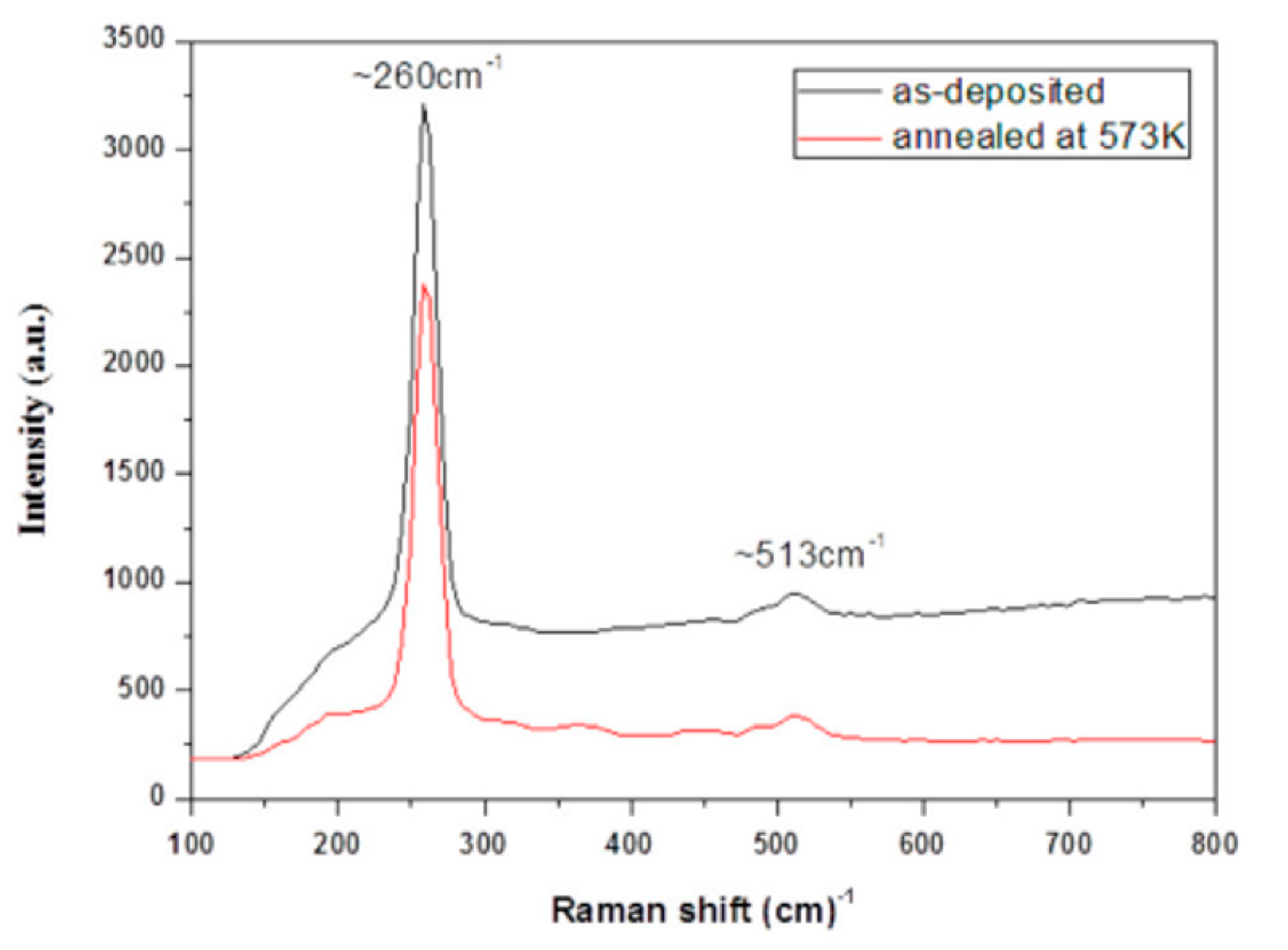
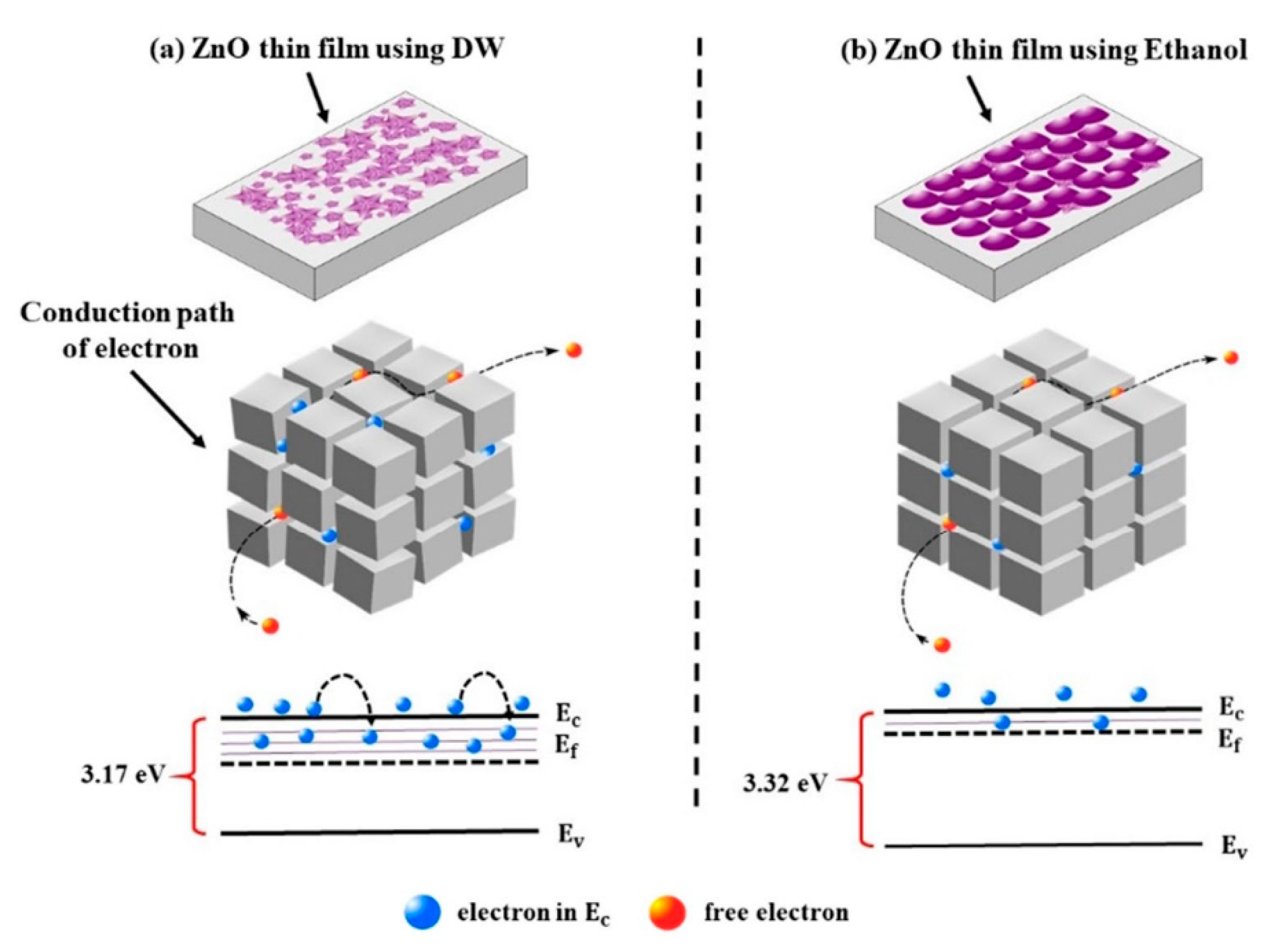
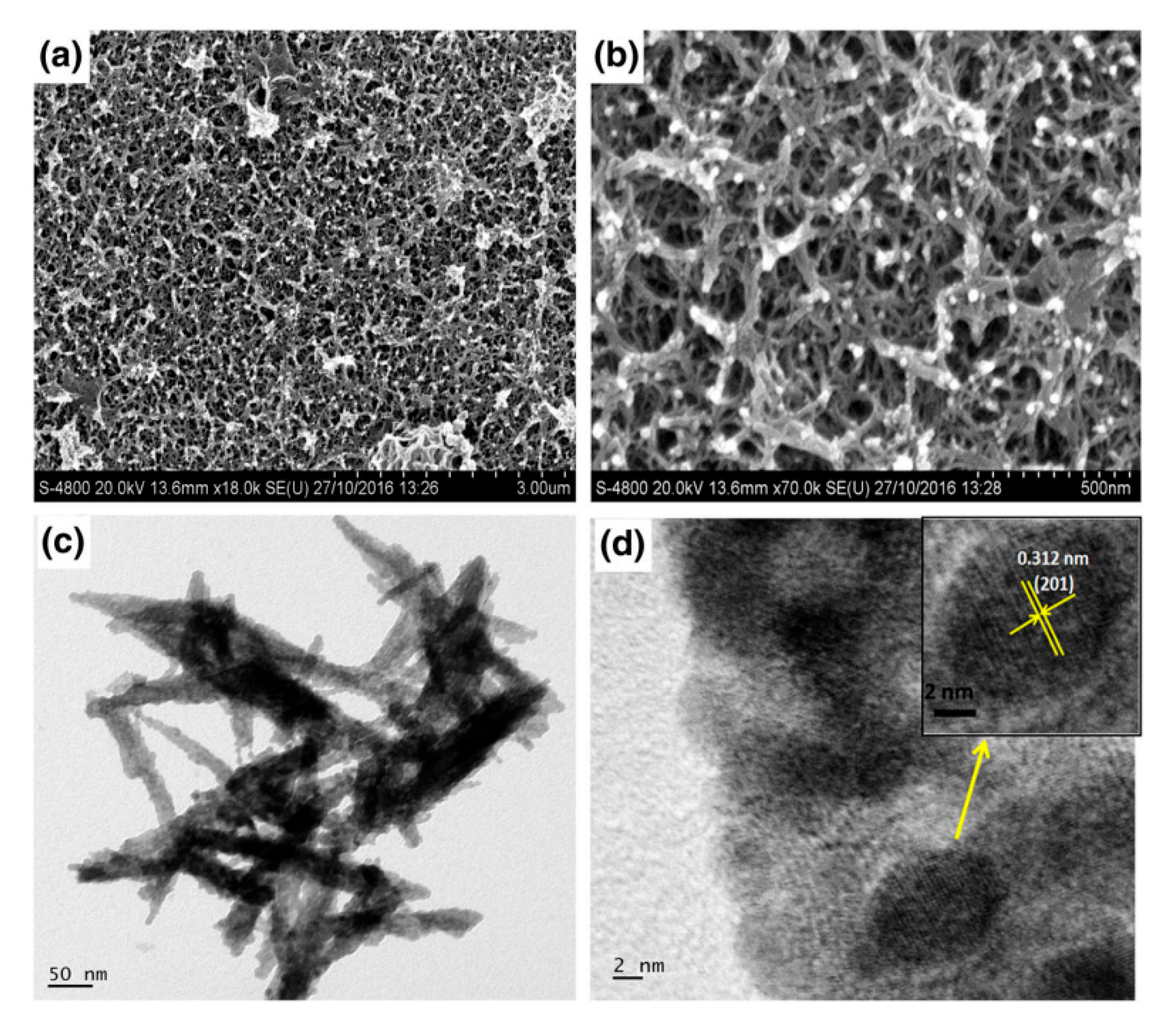
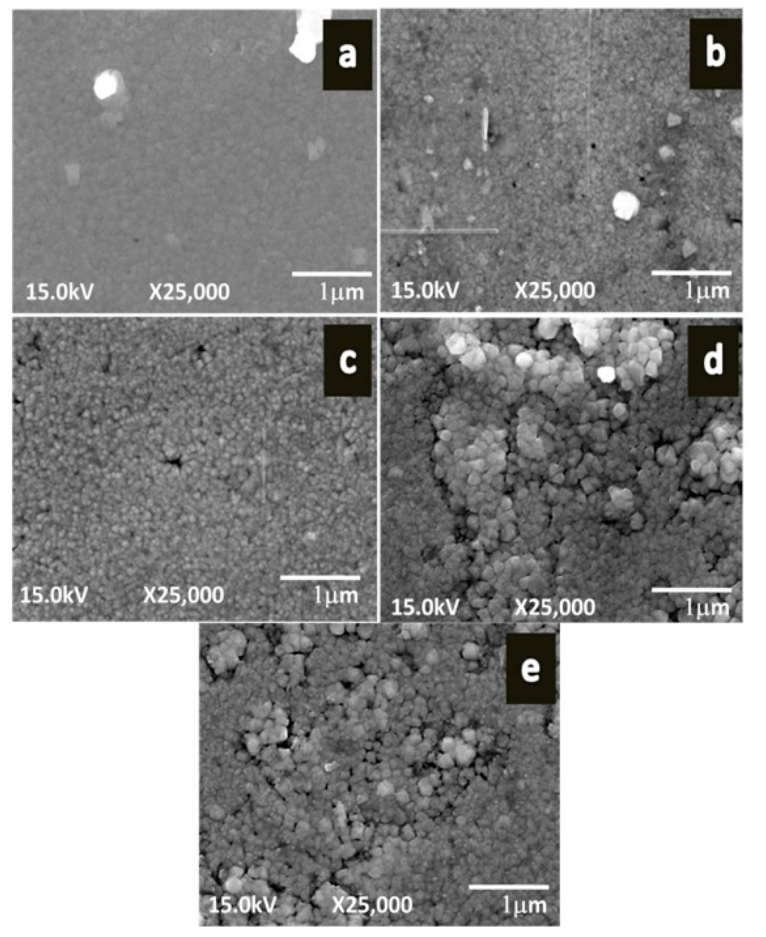
5.1. Zinc Oxide Films

Zinc oxide films were deposited onto various substrates, such as copper (Cu), silicon (Si), and glass slides [131]. Morphological studies revealed nano-prisms, small flowers, and rods were observed in glass, silicon, and copper substrates, respectively. In XRD patterns, it was found that two, three, and four peaks could be detected in silicon, glass, and copper substrates. However, all the films showed the wurtzite phase with a very sharp peak in the (002) plane. Sreedev and co-workers [132] described the produced ZnO films (15 deposition cycles), treated under 450 °C for 60 min. These films showed lower percentages of absorbance and transmittance values in the visible region. Bijoy and co-workers [133] highlighted the films deposited on soda lime glass showing three peaks (2θ = 31.74°, 34.4°, and 36.21°) with the hexagonal wurtzite structure. Major peaks corresponded to the (101) plane for the post-annealed films (250 °C, 60 min, air atmosphere) deposited on copper foil. Morphological characterization confirmed bigger grain sizes for films grown on the soda lime glass (260–300 nm) than copper foil samples (200–230 nm). Optical characterization showed that a 35–65% transparency in the visible range could be observed (soda lime glass). Further, they explained that the transparency improved and the absorption edge shifted from 350 to 380 nm upon the post-annealing process. The flower-like morphology and zincite hexagonal structure (crystalline size = 10–11.85 nm, thickness = 510 nm) could be seen in the films deposited on silica glass substrates by using ZnSO4, ammonia, and thiourea [134]. These films could be used in solar cell applications due to the suitable band gap (3.2 eV) and moderately high transmittance in the visible region. The growth of the ZnO film (by using ethanol or distilled water) was proposed by Yergaliuly and co-workers [135] as highlighted in Equations (41)–(44).
ZnCl 2 + 2 NH 4 OH Zn OH 2 + 2 N H 4 C l
Zn OH 2 + 4 NH 4 + 2 H 2 O + 2 H + + [ Zn ( NH 3 ) 4 ] 2 +
[ Zn ( NH 3 ) 4 ] 2 + + 4 H 2 O   Zn OH 2 + 2 OH + 4 NH 4 +
Zn OH 2 ZnO + H 2 O
Experimental results showed that a higher band gap (3.32 eV) was observed in the films grown with ethanol due to an increase in the carrier concentration. Figure 8 indicates rougher and smoother surfaces in the random oriented grains (using distilled water (DW) and well aligned along the c-axis (using ethanol (C2H5OH), respectively. It was noted that the Fermi level successfully moved to a higher energy level (significantly above the minimum of the conduction band). The influence of the number of cycles on the morphology of films was reported by Garza and co-workers [136]. Firstly, nuclei were observed in the sample. Then, nucleation and growth processes were carried out. Finally, a flower-like structure was observed They explained that the greater number of petals with bigger diameters could be seen with the increasing number of cycles (1, 3, 5, and 10 cycles).

5.2. Titanium Oxide Films

Titanium (III) chloride and ammonium hydroxide (NH4OH) solution were used to produce TiO2 films on ITO glass substrates at 300 K, under 250 deposition cycles [137]. The growth rate was 0.6 nm/cycle during the experiment, based on the XRD analysis, the presence of TiO2 with Ti3O5 and beta phase titanium dioxide or titanium (IV) oxide (TiO2) in as-deposited films and annealed films, respectively. SEM studies confirmed compact morphology with spherical grains (20–50 nm). In photoelectrochemical studies, annealed films (450 °C, 6 h) indicated more photoactivity and stability in electrolytes than as-deposited films. Oommen and co-workers [138] reported the growth rate was 0.01–0.02 nm/cycle, with the film thickness about 0.3 to 1.2 µm. The films annealed at 300 °C showed amorphous phases, while annealed films (400 °C) successfully improved the crystallinity of the films in the XRD studies. Based on the optical characterization, direct (3.4 to 3.8 eV) and indirect band gap values (2.1 to 3.8 eV) increased with the annealing process. Garcia and co-workers [139] explained the mechanism of film formation via titanium (III) chloride (TiCl3) (source of Ti3+) and hot water (source of oxygen) under 150 cycles, at 353 K, as highlighted in Equations (45)–(47).
4 Ti 3 + + O 2 + 2 H 2 O 4 H + + 4 TiO 2 +
TiO 2 + + H 2 O 2 H 2 O + Ti ( O 2   ) 2 +
TiO 2 + + OH H + + TiO 2
SEM studies confirmed bigger grain sizes in as-deposited films (228 nm) compared to annealed films (203 nm) because of the water evaporation in the annealing process. Moreover, flower-like morphology could be detected because grain coalescence caused them to grow. Fluorine-doped tin oxide-coated glass was used as the substrate during the formation of films [140]. Spherical grains with irregular shapes could be observed in SEM images. In the surface wettability analysis, these films were hydrophobic in nature (water contact angle more than 90°). TEM images confirmed chain-like structures with small particles as reported by Agnes and co-workers [141]. Patil and co-workers [142] described the synthesis of films by using TiCl3 and sodium hydroxide (NaOH). They observed (a) a higher growth rate when a higher concentration of precursor was used, and (b) poor quality of the films due to powdery deposits. They suggested that the obtained films be heated at 673 K for 120 min to remove hydroxide and improve the crystallinity.

5.3. Cadmium Oxide Films

Cadmium acetate and hydrogen peroxide (H2O2) were used to produce adherent and dark yellowish color films [143]. The films deposited in higher molarity (0.06 M) showed bigger grain sizes, excellent crystallinity, high absorbance values, and compact distribution over the surface of the substrates compared to lower molarity (0.03 M). The cadmium chloride was used to prepare thin films on microscopic glass slides [144] at room temperature under various deposition cycles (40 cycles to 120 cycles); the thin film formations could be highlighted in Equations (48)–(51).
CdCl 2 + 2 NaOH Cd OH 2 + 2 NaCl
Cd OH 2 + NaOH H 2 O + H + + NaCdO 2
H + + NaCdO 2 + H 2 O NaOH +   Cd OH 2
Cd OH 2 + heat CdO + H 2 O
The XRD analysis showed that the highest intensities and biggest crystallize size (13.59 nm) could be observed when the deposition cycle was 80 cycles. The spongy cluster and band gap energy were reduced; however, absorbance increased, with the increasing number of deposition cycles. The annealing effect (623 K, 120 min, air atmosphere) on the properties of the thin films was studied by Salunkhe and co-workers [145]. A lower band gap (3.3 eV), smaller crystallite size (20–30 nm), lower electrical resistivity, and uniform coverage of the substrate surface could be seen in the as-deposited films when compared to annealed films. Cadmium acetate (0.1 M and 0.05 M) and ammonium hydroxide were used to synthesize thin films on glass slides [146]. The crystallize size (24.05 to 42.09 nm), thickness (410 to 424 nm), and band gap (2.17 to 2.21 eV) increased, but the strain (2.255 to 1.291 × 10⁻³) and dislocation density (17.277 to 5.643 × 10¹⁴) reduced with the increase in the solution concentration.

5.4. Iron Oxide Films

Formation of the amorphous phase and hydrous (water contact angle smaller than 10°) could be observed in Fe2O3 films [147]. These materials could be considered potential candidates for supercapacitor applications due to their excellent supercapacitance values (178 F/g at a scan rate of 5 mV/s). The annealing effect on the Fe3O4 films was studied by Sheik and co-workers [148]. The crystallite size and transmission in the UV-visible region increased, and spherical morphological agglomeration could be observed with the annealing of the films. The iron(II) sulfate (FeSO4) and NH4OH were used to produce magnetite (Fe3O4) films under various deposition temperatures [149]. The XRD studies showed a cubic phase, Fd3m space group, and prominent growth direction (311) plane. Researchers also described the average crystallite size (56.34 to 34.73 nm) as reduced, but the dislocation densities (3.15 to 8.29 × 10¹⁴/m2), microstrain (35.12 to 46.85 × 10⁻⁴), and intensities of the emission peaks in photoluminescence spectra increased by increasing the deposition bath temperature from 55 °C to 85 °C. Based on the photoluminescence response, four peaks, around 360 nm (transition between vibrational energy), 442 and 492 nm (intraband defects of doubly ionized oxygen), 520 nm (singly ionized oxygen vacancies), and 592 nm (oxygen interstitials) could be detected in the obtained films. The Fe2O3 films were synthesized on glass slides as reported by Ozge [150]. The refractive index and band gap values were 1.45–3.23 (400–700 nm, visible range) and 2.62–2.68 eV, respectively. The XRD and FESEM analyses revealed non-crystalline and porous morphology, respectively.

5.5. Tin Oxide Films

The SnO2 films were deposited on glass slides and were annealed at 450 °C for 120 min [151]. These films indicated maximum conductivity, a film thickness of about 263 nm, and the least sheet resistance of 141 kΩ. The deposition of films was conducted by using ethylene diamine (C2H8N2) (complexing agent) on glass substrates [152]. The annealing treatment can improve the crystallinity and reduce strain in the crystal lattice. Further, these films indicated excellent optical transparency in the 200–1000 nm region. Yunus and co-workers [153] reported the synthesis of thin films on glass slides at room temperature. The XRD and SEM studies revealed tetragonal structurals, and grains were covered well on the substrate surfaces. The band gap reduced (3.9 to 3.54 eV), the electrical conductivity changed (0.015–0.815 Ω−1⋅cm−1), while surface morphology and crystallinity improved when the film thickness increased (215 to 490 nm). Joohee and co-workers [154] proposed the growth of SnO2 films on glass substrates by using tin (II) chloride and H2O2 solutions under various deposition cycles. Experimental results showed that film thickness (12 to 50 nm), crystallite size, and mobility of the films increased; however, transmittance reduced (92% to 85%) with the increasing deposition cycle (from 20 to 60 cycles).

5.6. Nickel Oxide Films

The nickel oxide nanostructured films were deposited on glass slides at room temperature [155]. The band gap (3.71 to 3.67 eV) and resistivity (4.1 to 802.1 Ω·cm) were observed to strongly depend on the film thickness. The annealing effect on the properties of films was investigated by Tuba and co-workers [156]. Research findings showed that the crystal and surface properties were well-developed in the annealed films. The band gap (3.3 to 3.11 eV) was reduced by increasing the annealing temperature from 200 °C to 400 °C. Nickel oxide films could be used in supercapacitor applications due to the highest specific energy (64.8 Wh/kg) and excellent specific capacitance (1341 F/g); they showed long-term cycle stability with 90% capacitance retention after 1000 deposition cycles [157]. Nickel (II) chloride was used to produce films on glass substrates as described by Sandesh and co-workers [158]. The obtained films were polycrystalline and consisted of platelet-type morphology. The films showed a good response (72%) to 5000 ppm liquefied petroleum gas at lower operating temperatures.

5.7. Zirconium-Doped Cadmium Oxide Films

Zirconium-doped cadmium oxide thin films were deposited on stainless steel substrates by Agnes and co-workers [159]. The SEM analysis showed that grain sizes were reduced by increasing the dopant percentages during the experiment. The 2%-doped cadmium oxide films showed the best electrochemical features, with a band gap of about 2.07 eV and a cubic phase, and they could be used in optoelectronic devices.

5.8. Copper Nickel Oxide Films

The CuxNix−1O(x = 0, 0.25, 0.5, 0.75, 1) nanostructured films were deposited on amorphous glass slides [160]. The band gap (3.34 to 2.01 eV) was reduced, and smoother films could be observed with the increase of copper (Cu) concentration during the experiment.

5.9. Tungsten-Doped Zinc Oxide Films

Tungsten-doped zinc oxide films were deposited on the glass substrate [161]. The obtained films showed a hexagonal wurtzite structure and uniform morphology based on XRD and SEM analyses. When the amount of tungsten (W) increased, the band gap increased and the band edge emission moved towards the blue region.

5.10. Copper-Doped Zinc Oxide Films

Cu-doped ZnO films were deposited under various concentrations of copper solutions (0.05 and 0.1 mol%) [162]. The rod-like shape and hexagonal wurtzite structure could be seen based on XRD and SEM studies. The surface roughness, band gap, and green emission reduced, but the intensity of the UV emission increased with the increase of copper concentrations according to atomic force microscopy, ultraviolet spectroscopy, and photoluminescence studies.

5.11. Strontium-Doped Zinc Oxide Films

The strontium (Sr)-doped ZnO films were deposited on the substrates under various concentrations of strontium [163]. SEM and XRD studies showed the flower-like morphology and crystal orientation transformation occurred (from the (002) to the (101) plane) with doping concentrations. During the experiment, the band gap increased (3.02 to 3.2 eV) and enhanced the ammonia gas sensing behavior with the increasing strontium concentration.

5.12. Nickel-Doped Zinc Oxide Films

The nickel (Ni)-doped zinc oxide films were prepared on glass substrates under various concentrations of nickel (1, 3, and 5%) [164]. The Fourier transform infrared analysis confirmed the presence of different functional groups in the obtained films.

5.13. Cobalt-Doped Nickel Oxide Films

Taskopru and co-workers [165] reported on the transparent Co-doped nickel oxide films [2015] deposited on glass substrates. The XRD studies confirmed polycrystalline, the cubic phase, and the most intense peaks corresponding to the (111) and (222) planes. No significant move in the Raman spectrum could be seen and the structure was not changed during the cobalt (Co)-doping process.

5.14. Cobalt-Doped Manganese Oxide Films

The cobalt-doped manganese oxide films (Co:Mn3O4) were deposited on soda lime glass substrates [166] at room temperature by using manganese (II) chloride tetrahydrate (MnCl2.4H2O), ammonium hydroxide, and cobalt(II) chloride tetrahydrate (Cl2CoH8O4). The XRD results highlight that the most intense orientation changed from the (002) to the (211) plane with increasing the cobalt concentration from 0.5% to 3%.

5.15. Manganese-Doped Copper Oxide Films

The manganese (Mn)-doped CuO films were deposited on glass substrates [167]. Experimental findings described plate-like morphology and a monoclinic structure. The shapes of the nanostructures changed and the band gap increased when the concentration of Mn increased.

5.16. Manganese Oxide Films

The amorphous manganese oxide films were produced on glass substrates [168]. Experimental results showed the highest specific capacitance was 243 F/g when the scan rate was 10 mV/s. Moreover, two peaks could be observed in the cyclic voltammogram attributed to Mn2+ and Mn3+, respectively. Highly adherent and compact morphology of films were produced by Mangesh and co-workers [169]. Researchers concluded that hausmannite (Mn3O4) films were changed to manganese dioxide (MnO2) after chemical treatments (with hydrochloric acid (HCl) solution). The obtained films showed different specific capacitance values through electrochemical transformation (72 to 393 F/g) and chemical transformation (72 to 258 F/g). Enhanced physical properties (from amorphous to crystalline, irregularly fused capsule-like grains) improved the band gap and transmittance of SILAR-deposited Mn3O4 films decorated on graphene [170]. The films showed the highest specific capacitance (194 F/g), indicating these materials could be used in electrochemical storage devices. Malavekar and co-workers [171] reported that the SILAR-deposited MnO2 films (tetragonal and birnessite phase) could be used in supercapacitor devices. Waikar and co-workers [172] proposed synthesizing thin films under different cationic precursors. The films prepared using manganese (II) acetate showed spike morphology; the contact angle was 35° and the specific capacitance was 222 F/g (5 mV/s csan rate). The films produced using manganese (II) chloride (MnCl2) indicated void morphology, the contact angle was 26°, the specific capacitance was 375 F/g, (5 mV/s csan rate), the maximum energy density was 17 Wh/kg, and the power density was 999 W/kg. The films synthesized from manganese sulfate (MnSO4) exhibited porous morphology, the contact angle was 29°, and the specific capacitance was 248 F/g, (5 mV/s csan rate). The experimental results concluded the best electrochemical properties by using manganese (II) chloride and retained stability of 94% after 4500 cyclic voltammetry cycles. NaOH and MnSO4 were used to produce thin films on a stainless steel substrate at 273 K, the rinse time was 10 s, and the immersion time was 20 s [173]. In the FTIR studies, 615, 499, 3746, and 1544 cm−1 contributed to MnO in tetrahedral, the MnO band in octahedral, and the stretching and bending vibrations of hydroxide (OH) molecules, respectively. In the TEM studies, the nanorod-like structure, d-spacing of 0.26 nm, and tetragonal phase could be observed in the films deposited at 75 deposition cycles.

5.17. Tungsten Oxide Films

Preparation of the tungsten oxide solution (WO3) thin films on stainless steel substrates by using NaOH (as an anionic source) and oxotungsten hydrate (WO.H2O, as a cationic source)) took place at room temperature [174]. The obtained films were annealed under 673 K for 180 min to remove hydroxide and improve the crystallinity of the obtained thin films. The film thickness increased with the number of deposition cycles (until 100 cycles) due to the growth of nucleation and the coalescence process, reached maximum thickness (0.08 mg/cm2), and finally these films were peeled off. The XRD studies showed monoclinic phases with a crystallite size of about 45 nm based on the (200) plane. In the SEM analysis, rod-like morphology with an average width of 1–2 µm could be detected. In the optical studies, the obtained films had band gaps of 2.5 eV and showed excellent absorbance of light in the visible range. In the cyclic voltammogram, the specific capacitance and interfacial capacitance were 266 F/g (scan rate = 10 mV/s) and 0.0214 F/cm2, respectively. Lastly, the electrical parameters, including coulombic efficiency (92%), specific energy (55.68 Wh/kg), and specific power (10.12 kW/kg) were reported.

5.18. Silver-Doped Zinc Oxide Films

The p-type silver (Ag)-doped ZnO films were synthesized on glass slides under various deposition cycles [175]. The film thickness (0.34 to 0.49 µm) absorbance value increased (due to the accumulation of a new layer on the substrate), but the band gap reduced (2.91 to 2.49 eV) with the increasing deposition cycle (from two to four cycles). In the SEM analysis, the films prepared under four cycles showed smooth surfaces with smaller grains, completely covered on the surface of the substrate.

5.19. Indium-Doped Zinc Oxide Films

The In-doped ZnO thin films were synthesized on glass and p-type silicon substrates [176] at 100 deposition cycles. The biggest grain size could be observed when the indium concentration was 2.5%, while small and more uniform morphology took place at a higher doping concentration (7.5%) based on the FESEM images. The structural analysis, such as crystallite size (69.3 to 67.5 nm), reduced, but the microstrain (1.67 to 1.73 × 10⁻³) and dislocation density (2.08 to 2.19 × 10¹³, lines/m2) increased, and were reported for the films prepared at various In-doping concentrations (from 2.5% to 7.5%). Transparency increased initially and then dropped at a higher indium (In) concentration because of the structural disorders (inclusion of more indium) in the obtained samples.

5.20. Aluminum Oxide Films

Aluminum oxide showed some excellent properties. including friction resistance, heat resistance, and corrosion resistance. The aluminum oxide or aluminum (III) oxide (Al2O3) films were deposited on aluminum substrates at room temperature in the experiment [177]. The obtained films showed hydrophobic properties with contact angles of 117°. SEM studies revealed non-uniform morphology and rougher surface.

5.21. Aluminum-Doped Zinc Oxide Films

Aluminum (Al)-doped zinc oxide films were produced under various dipping cycles [178]. The XRD analysis showed the hexagonal phase, and the intensities of the samples increased when the dipping cycle increased. Small grain sizes and smoother morphology could be observed in all films based on the SEM images. The photoluminescence (PL) spectra indicated that good films (lesser defect density) could be seen when the deposition cycle was 30 cycles. The optical transmittance was 87% in the visible region, while the band gap was 3.23 eV.

5.22. Bismuth Oxide Films

The formation of Bi2O3 on stainless steel took place by using bismuth(III) nitrate (cationic) and double distilled water (anionic) under 80 deposition cycles. The growth of the films was described by Shrikant and co-workers [179], as highlighted in Equations (52)–(54).
Bi ( NO 3 ) 3 .5 H 2 O + N ( CH 2 CH 2 OH ) 3 BiN ( CH 2 CH 2 OH ) 3 ] 3 + + 5 H 2 O + 3 ( NO 3
[ BiN ( CH 2 CH 2 OH ) 3 ] 3 + Bi 3 + + N ( CH 2 CH 2 OH ) 3
2 Bi 3 + + 6 OH 3 H 2 O + Bi 2 O 3
XRD studies highlighted the cubic phase; two strong peaks (2θ = 28° and 33°) appeared. Several peaks could be seen in the FTIR, including 844 cm−1 (stretching vibration of Bi-O-Bi), 1058 cm−1 (stretching vibration of the Bi-O bond), 1321 cm−1 (stretching vibration of Bi-O- bond), and 3440 cm−1 (O-H stretching). TEM and SEM analyses revealed well-distributed needles with smaller particle sizes (5–10 nm) on the substrate. The interplanar spacing was 0.312 nm and contributed to the (201) lattice plane as indicated in the HR-TEM image (Figure 9). The findings showed that the best specific capacitance was 329.6 F/g when the scan rate was 5 mV/s (1M Na2SO4 electrolyte), while the retention capacity was 72% after 3000 cycles.

5.23. Copper Oxide and Cuprous Oxide Films

The p-type Cu2O (cuprous oxide or copper (I) oxide) films were deposited on the substrates at 70 °C, and then annealed under various temperatures (100 to 500 °C) for 60 min [180]. The phase transition could be observed (Cu2O to CuO) at 300 °C. The resistivity values were calculated to be 6.12 × 10⁴ Ω·cm and 8.23 × 10³ Ω·cm, respectively. Lohar and co-workers [181] revealed that the copper (II) oxide or cupric oxide (CuO) thin films were monoclinic structures, as well as the formation of nanorod morphology. The photoluminescence spectra and photoelectrochemical cell indicated strong peaks (465 and 516 nm) and power conversion efficiency of 0.26% for 100 deposition cycles. The cuprous oxide nanorods were prepared on soda lime glass substrates in the presence of sodium chloride (NaCl) [182]; the chemical reactions could be explained in Equations (55) and (56).
Cu S 2 O 3 Cu + + S 2 O 3 2
2 Cu + + 2 OH H 2 O + Cu 2 O
Raman spectroscopy confirmed the characteristic peaks (143, 214, 280, 332, and 620 cm−1) corresponding to the Cu2O phase. The XRD and SEM analyses indicated polycrystalline (in nature) with the (111) plane and spherical grains, respectively. The crystallite sizes (15.94 to 14.14 nm) and resistivity (15,142 to 685 Ω·cm) reduced, but the dislocation density (3.94 × 10⁻³ to 5 × 10⁻³) and strain (2.17 to 2.45 × 10⁻³) increased with the increasing concentration of NaCl (0 to 6 mmol). The electrical properties of the as-deposited films, such as sheet resistance (1.27 to 33.46 MΩ/square), surface resistivity (685 to 15,142 Ω·cm), activation energy (0.14 to 0.21 eV), and band gap energy (1.96 to 2.36 eV) were reported under different contents of the NaCl electrolyte (0 to 8 mmol). Rafea and co-workers [183] suggested that amorphous films were annealed up to 823 K. The nano-spherical grain sizes (SEM) and crystalline sizes (XRD) were 50–100 nm and 14–21 nm, respectively. The band gap values in the as-deposited films and annealed films (373 K) were observed at about 2.3 and 2.4 eV. The lower band gaps for the films annealed were at 373–673 K (1.85 eV) and 673–823 K (1.7 eV). Lee and co-workers [184] described the growth of Cu2O films on glass slides by using copper thiosulfate and NaOH. Anneal films were produced under different temperatures and times. The summaries of the band gap, resistivity, carrier concentration, mobility, and crystalline structure (Table 3) were highlighted by researchers. The fluorine-doped tin oxide glass was used as the substrate during the formation of Cu2O thin films [185]. The XRD and SEM results showed the most intense peak corresponding to the (111) plane and micro-crack morphology, respectively. Experimental findings showed that electrical resistivity and the band gap were reduced when the pH of the cationic solution was reduced.

5.24. Cobalt Oxide Films

Cobalt oxide films could be used in biomedical devices, sensing, and electronics due to stable catalytic activity, high saturation magnetization, and excellent electrochemical performance. Cobalt chloride was used to produce thin films at room temperature [186]. The electrochemical supercapacitive properties revealed that the highest specific capacitance was 165 F/g when the scan rate was 10 mV/s.

5.25. Zinc Iron Oxide Films

The ZnFe2O4 thin films were produced in the absence of a surfactant [187]. A porous surface with nanoplate particles could be observed. The obtained film exhibited a specific capacitance of 471 F/g when the scan rate was 5 mV/s, in a 1 M NaOH solution. The researcher also highlighted the voltage window (1 V), power density (277 W/kg), energy density (4.47 Wh/kg), and long cycle life in solid state symmetric supercapacitor devices.

6. Conclusions

Metal sulfide, metal selenide, metal oxide, and metal telluride thin films were successfully prepared on various types of substrates by using the SILAR deposition technique. Experimental results confirmed that these materials could be used in solar cells, supercapacitors, and sensor applications. Thin films of good quality could be produced after optimizing different experimental conditions, such as the deposition cycle, complexing agent, precursor concentration, rinse time, temperature, annealing process, and immersion time.

Funding

This research was funded by INTI International University, Malaysia.

Institutional Review Board Statement

Not applicable.

Informed Consent Statement

Not applicable.

Conflicts of Interest

The author declares no conflict of interest.

References

  1. Harif, N.; Halina, M.; Hasrul, R.; Kazi, S.; Camellia, D.; Sopian, K.; Amin, N. The role of deposition temperature in the photovoltaic proeprties of RF sputtered CdSe thin films. Crystals 2021, 11, 73. [Google Scholar] [CrossRef]
  2. Megan, J.; Kreiml, P.; Mitterer, C. Materials engineering for flexible metallic thin film applications. Materials 2022, 15, 926. [Google Scholar] [CrossRef]
  3. Ho, S.M.; Mandati, S.; Chandran, R.; Mallik, A.; Arif, S.; Deepa, K. preparation of CuInSe2 thin films by using various methods (a short review). Orient. J. Chem. 2019, 35, 1–13. [Google Scholar]
  4. Bin, W.; Huang, W.; Lin, W.; Lee, H. Study on optical and electrical properties of thermally evaporated tin oxide thin films for perovskite solar cells. Crystals 2021, 11, 1380. [Google Scholar] [CrossRef]
  5. Zaman, M.; Taru, C.; Dehury, K.; Rajaram, P. Synthesis and characterization of spin coated ZnS thin films. AIP Conf. Proc. 2018, 1953, 100066. [Google Scholar] [CrossRef]
  6. Ho, S.M. Studies of power conversionefficiency and optical properties of Ni3Pb2S2 thin films. Makara J. Sci. 2017, 21, 119–124. [Google Scholar]
  7. Mikayal, A.; Zarine, S.; Gohar, S.; Ladimir, A.; Artak, S. Gas senor based on ZnO nanostructured film for the detection of ethanol vapor. Chemosensors 2022, 10, 245. [Google Scholar] [CrossRef]
  8. Istrate, A.; Vulpe, S.; Florin, N.; Lucia, M.; Cosmin, R.; Oana, T. Ca-doped ZnO:Al thin films: Synthesis and characterization. Coatings 2021, 11, 1023. [Google Scholar] [CrossRef]
  9. Agustin, L.; Rosa, M.; Cesia, G.; Isaac, R.; Felipe, C.; Edith, O.; Ricardo, A. Automated instrument for the deposition of thin films using successive ionic layer adsorption and reaction. Processes 2022, 10, 492. [Google Scholar] [CrossRef]
  10. Jose, O.; Jorge, S.; Acros, M.; Omar, R.; Bustos, E.; Gonzalez, M. Design and development of software for the SILAR control process using a lost-cost embedded system. Processes 2021, 9, 967. [Google Scholar] [CrossRef]
  11. Sundhar, A. Development of ZnS thin film with Co, Cu and Ag dopingusing SILAR method. Mater. Today Proc. 2022, 48, 377–381. [Google Scholar] [CrossRef]
  12. Mahesh, K.; Send, K.; Kuar, M.; Panda, B. Chlorophyll a functionalized ZnCdS thin flm fabricated by SILAR technique for dye sensitized solar cells. Inorg. Chem. Commun. 2022, 142, 109670. [Google Scholar] [CrossRef]
  13. Saba, F.; Sabah, I.; Salim, A.; AlOgaili, H. Influence of deposition time on absorption and electrical characteristics of ZnS thin films. Optik 2022, 260, 169056. [Google Scholar] [CrossRef]
  14. Pathan, M.; Salunkhe, V.; Sankapal, B.; Lokhande, D. Photoelectrochemical investigation of Ag2S thin films deposited by SILAR method. Mater. Chem. Phys. 2001, 72, 105–108. [Google Scholar] [CrossRef]
  15. Vijendra, A.; Dargad, S.; Rajesh, A.; Govind, K. Fabrication of Highly Conducting Ag2S Thin Films on FTO Substrate by Using SILAR. Adv. Mater. Res. 2022. [Google Scholar] [CrossRef]
  16. Lokhande, C.; Sankapal, B.; Mane, R. A new chemical method for the preparation of Ag2S thin films. Mater. Chem. Phys. 2000, 63, 226–229. [Google Scholar]
  17. Kakade, B.; Nikam, P.; Gosavi, R. Effect of immersion cycles on structural, morphology and optoelectronic properties of nanocrystalline Ag2S thin films deposited by SILAR technique. IOSR J. Appl. Phys. 2014, 6, 6–12. [Google Scholar]
  18. Gosavi, R.; Patel, S.; Patil, R.; Jadhav, M. Studies on Characterization of Nanocrystalline Silver Sulphide Thin Films Deposited by Chemical Bath Deposition (CBD) and Successive Ionic Layer Adsorption and Reaction (SILAR) method. Arch. Phys. Res. 2011, 2, 27–35. [Google Scholar]
  19. Sadovnikov, S.; Gusev, A.; Rempel, A. Nanocrystalline silver sulfide Ag2S. Rev. Adv. Mater. Sci. 2015, 41, 7–19. [Google Scholar]
  20. Shen, H.; Jiao, X.; Oron, D.; Lin, H.; Li, J. Efficient electron injection in non-toxic silver sulfide (Ag2S) sensitized solar cells. J. Power Sources 2013, 240, 8–13. [Google Scholar] [CrossRef]
  21. Ambily, K.; Ali, K.; Geetha, V.; Kannan, P. Towards phase pure CZTS thin films by SILAR method with augmented Zn adsorption for photovoltaic application. Mater. Renew. Sustain. Energy 2019, 8, 16. [Google Scholar] [CrossRef]
  22. Kumar, G.; Balaji, P.; Gnana, P.; Kaushik, R.; Shriram, M. Investigations on SILAR coated CZTS thin films for solar cells applications. Phase Transit. 2021, 94, 556–566. [Google Scholar] [CrossRef]
  23. Gayatri, B.; Das, S.; Ghosh, S. Optical Properties of Cu2ZnSnS4 (CZTS) Made By SILAR Method. Mater. Today Proc. 2019, 18, 494–500. [Google Scholar]
  24. Sawanta, M.; Patil, P.; Oh, W.; Betty, A.; Shinde, S. Synthesis and characterization of Cu2ZnSnS4 thin films by SILAR method. J. Phys. Chem. Solids 2012, 3, 735–740. [Google Scholar]
  25. Suryawanshi, P.; Patil, S.; Shin, S.; Gurav, K.; Agawane, L.; Gang, G. The synergistic influence of anionic bath immersion time on the photoelectrochemical performance of CZTS thin films prepared by a modified SILAR sequence. RSC Adv. 2014, 4, 18537–18540. [Google Scholar] [CrossRef]
  26. Mane, S.; Lokhande, D.; Sankapal, B. Successive ionic layer adsorption and reaction (SILAR) method for the deposition of large area (∼10 cm2) tin disulfide (SnS2) thin films. Mater. Res. Bull. 2000, 35, 2027–2035. [Google Scholar]
  27. Mani, P.; Manikandan, K.; Prince, J. Influence of molar concentration on triethanolamine (TEA) added tin sulfide (SnS) thin films by SILAR method. J. Mater. Sci. Mater. Electron. 2016, 27, 9255–9264. [Google Scholar] [CrossRef]
  28. Mitra, P.; Mukherjee, A. Structural and optical characteristics of SnS thin film prepared by SILAR. Mater. Sci. 2015, 33, 847–851. [Google Scholar]
  29. Biswajit, G.; Das, M.; Pushan, B.; Das, S. Fabrication and optical properties of SnS thin films by SILAR method. Appl. Surf. Sci. 2008, 254, 6436–6440. [Google Scholar]
  30. Qachaou, Y.; Daoudi, O.; Raidou, A.; Fahoume, M.; Lharch, M. The influence of solution temperature of SnS thin films grown by successive ionic layer adsorption and reaction (SILAR) method. IOP Conf. Ser. J. Phys. 2019, 1292, 012022. [Google Scholar] [CrossRef]
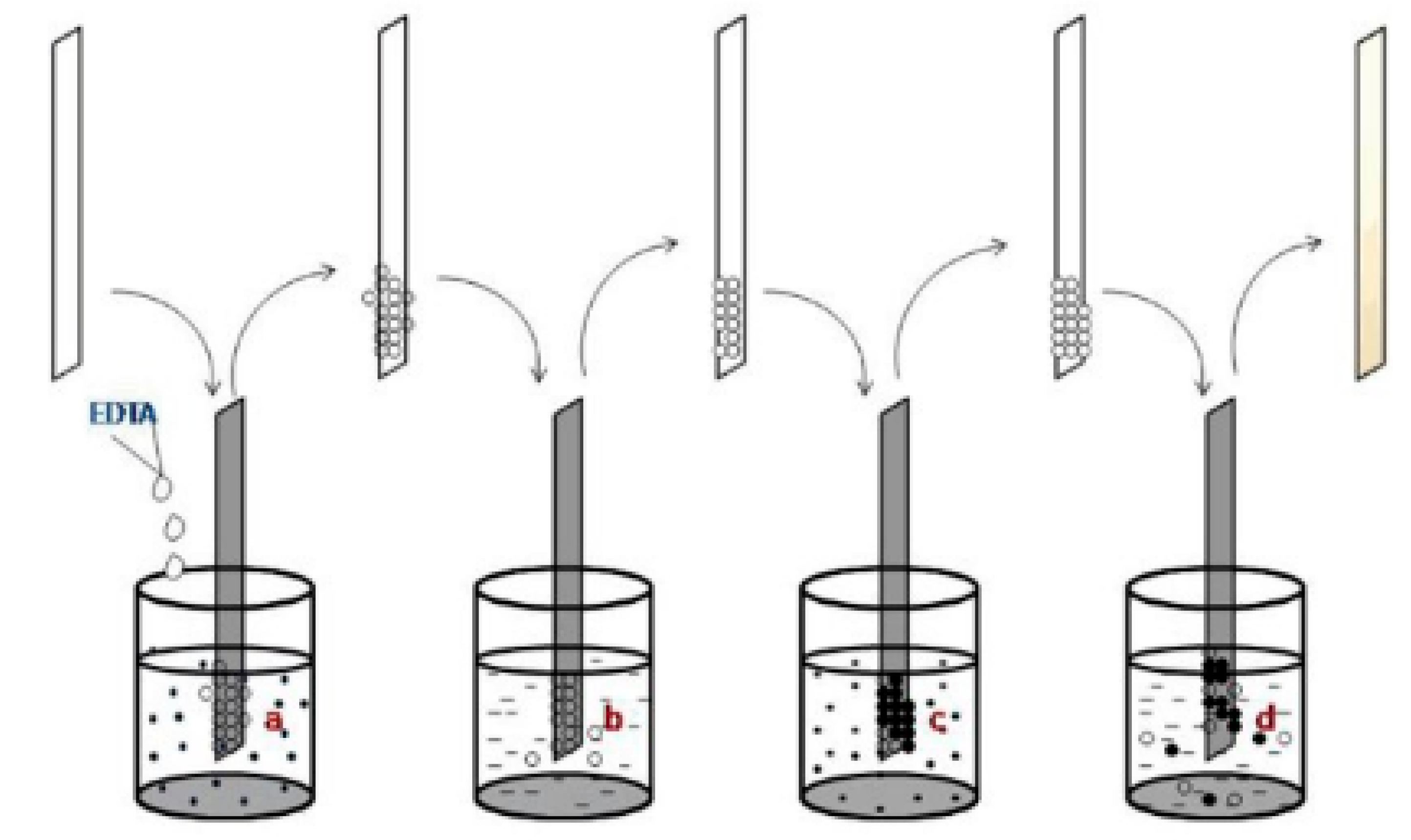
  31. Mani, P.; Joseph, P.; Manikandan, K. Influence of molar concentration on ethylene diamine tetra acetic acid (EDTA) added to tin sulfide (SnS) thin films grown by silar method. J. Mater. Sci. Mater. Electron. 2017, 28, 13602–13612. [Google Scholar] [CrossRef]
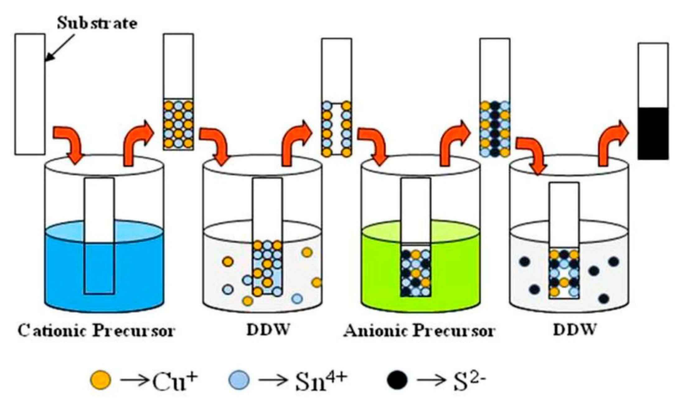
  32. Hao, G.; Shen, H.; Chao, G.; He, X. The influence of annealing atmosphere on the phase formation of Cu–Sn–S ternary compound by SILAR method. J. Mater. Sci. Mater. Electron. 2013, 24, 3195–3198. [Google Scholar]
  33. Harshad, D.; Lokhande, A.; Raut, V.; Patil, M.; Kim, H. Facile synthesis of Cu2SnS3 thin films grown by SILAR method: Effect of film thickness. J. Mater. Sci. Mater. Electron. 2017, 28, 7912–7921. [Google Scholar]
  34. Aykut, A. Structural and optical properties of Cu2SnS3 thin films obtained by SILAR method. Sakarya Univ. J. Sci. 2017, 21, 505–510. [Google Scholar]
  35. Shelke, H.; Patil, A.; Lokhande, C.; Kim, H. Electrochemical impedance analysis of SILAR deposited Cu2SnS3 (CTS) thin film. Int. J. Eng. Res. Technol. 2017, 10, 578–586. [Google Scholar]
  36. Kahraman, S.; Samed, C.; Haci, M.; Ali, C.; Salih, G. Cu2SnS3 absorber thin films prepared via successive ionic layer adsorption and reaction method. Int. J. Mater. Res. 2013, 104, 1020–1027. [Google Scholar] [CrossRef]
  37. Su, Z.; Sun, K.; Han, Z.; Liu, F.; Lai, Y.; Jie, L.; Liu, Y. Fabrication of ternary Cu–Sn–S sulfides by a modified successive ionic layer adsorption and reaction (SILAR) method. J. Mater. Chem. 2012, 22, 16346–16352. [Google Scholar] [CrossRef]
  38. Ashith, K.; Rao, K. Structural and Optical Properties of ZnS Thin Films by SILAR Technique obtained by acetate Precursor. IOP Conf. Ser. Mater. Sci. Eng. 2018, 360, 012058. [Google Scholar] [CrossRef]
  39. Haneefa, M.; Gani, M.; Fareed, S.; Raja, J. The studies on optical and structural properties of zinc sulfide thin films deposited by SILAR method. J. Chem. Pharm. Res. 2015, 7, 141–145. [Google Scholar]
  40. Mana, M.; Pankaj, K.; Habib, M. Fabrication and Characterization of ZnS based Photoelectrochemical Solar Cell. ES Energy Environ. 2020, 12, 77–85. [Google Scholar] [CrossRef]
  41. Geetha, V.; Rajan, V. Studies of Structural and Optical Properties of Zinc Sulphide Thin Films. Int. J. Mater. Phys. 2014, 5, 5–14. [Google Scholar]
  42. Roy, S.; Mitra, P. Preparation of ZnS thin film by Silar. Mater. Sci. Res. India 2008, 5, 447–452. [Google Scholar]
  43. Laukaitis, G.; Lindroos, S.; Leskela, M.; Rackaitis, M. Stress and surface studies of SILAR grown ZnS thin films on(100)GaAs substrates. Mater. Sci. Eng. A 2000, 288, 223–230. [Google Scholar] [CrossRef]
  44. Lindroos, S.; Bonnin, C.; Leskea, A.; Charreire, Y. Growth and Characterization of Zinc Sulfide Thin Films Deposited by the Successive Ionic Layer Adsorption and Reaction (Silar) Method Using Complexed Zinc Ions As the Cation Precursor. Mater. Res. Bull. 1998, 33, 453–459. [Google Scholar] [CrossRef]
  45. Trupti, T.; Abhishek, C.; Rahul, B.; Lokhande, D. Lanthanum sulfide/graphene oxide composite thin films and their supercapacitor application. SN Appl. Sci. 2018, 1, 110. [Google Scholar] [CrossRef]
  46. Sartale, D.; Lokhande, C. Growth of copper sulphide thin films by successive ionic layer adsorption and reaction (SILAR) method. Mater. Chem. Phys. 2000, 65, 63–67. [Google Scholar] [CrossRef]
  47. Obed, Y.; Dalia, A.; Zeuz, M. Deposition of Highly Crystalline Covellite Copper Sulphide Thin Films by SILAR. Phys. Status Solidi A Appl. Mater. Sci. 2017, 214, 1700500. [Google Scholar] [CrossRef]
  48. Seppo, L.; Arnold, A.; Markku, L. Growth of CuS thin films by the successive ionic layer adsorption and reaction method. Appl. Surf. Sci. 2000, 158, 75–80. [Google Scholar]
  49. Mani, P.; Janaki, A.; Seelan, A.; Prince, J.; Hameed, S.; Syed, S. Influence of Molar Concentrations on Optical Properties of Copper Sulphide Thin Films by Silar Method. Int. J. ChemTech Res. 2014, 214, 3573–3578. [Google Scholar]
  50. Ravindra, N.; Lee, Y.; Shm, J.; Roh, C.; Thi, T.; Sumanta, S. Chemical synthesis of 3D copper sulfide with different morphologies for high performance supercapacitors application. RSC Adv. 2016, 6, 14844–14851. [Google Scholar]
  51. Fouad, B.; Raidou, A.; Sall, T.; Larbi, L.; Ahmed, Q. Structural and optical properties of CdS thin films prepared by SILAR method. In Proceedings of the 2013 International Renewable and Sustainable Energy Conference (IRSEC), Ouarzazate, Morocco, 7–9 March 2013. [Google Scholar] [CrossRef]
  52. Dipalee, J.; Shaeed, S.; Farha, S.; Birajdar, R.; Anil, G.; Sharma, R. Effect of annealing on structural and optoelectronic properties of CdS thin film by SILAR method. Adv. Appl. Sci. Res. 2011, 2, 417–425. [Google Scholar]
  53. Hua, S.; Mu, J. SILAR Deposition of CdS Thin Films on Glass Substrates Modified with 3-Mercaptopropyltrimethoxysilane. J. Dispers. Sci. Technol. 2005, 26, 719–722. [Google Scholar] [CrossRef]
  54. Kester, O.; Tochukwu, M.; Kenneth, I.; Blssing, N. Influence of Dip Cycles on the Structural, Optical and Morphological Properties of CdS-SILAR Deposited Thin Films. J. NanoSci. NanoEng. Appl. 2016, 6, 19–26. [Google Scholar]
  55. Loreta, T.; Birute, S.; Albina, Z.; Leonas, N.; Selskis, A.; Norkus, E. Investigation of CdS Thin Films Deposition by the SILAR Method Using Cd(II) Organic Salt as Precursor. ECS Meet. Abstr. 2014, MA2014-02, 837. [Google Scholar] [CrossRef]
  56. Garadkar, K.; Patil, A.; Krake, P.; Hankare, P. Characterization of CdS thin films synthesized by SILAR method at room temperature. Arch. Appl. Sci. Res. 2010, 2, 429–437. [Google Scholar]
  57. Mitra, P.; Ayan, M.; Protim, P. Synthesis of Nanocrystalline CdS by SILAR and Their Characterization. J. Mater. 2014, 2014, 138163. [Google Scholar] [CrossRef]
  58. Joseph, O.; Ngozi, E.; Kelechi, N. Optical Properties of CuAl2S Alloyed Thin Films Prepared Using Enhanced Successive Ionic Layer Adsorption and Reaction Method. Int. J. Res. Innov. Appl. Sci. 2021, 6, 95–99. [Google Scholar]
  59. Fatma, G.; Serdar, U. Nickel doping effect on the structural and optical properties of indium sulfide thin films by SILAR. Open Chem. 2018, 16, 757–762. [Google Scholar]
  60. Anita, R.; Teny, J.; Sudha, K.; Vijayakumar, P. structural and Optical Properties of Indium Sulfide Thin Films Prepared by Silar Technique. Open Condens. Matter Phys. J. 2009, 2, 9–14. [Google Scholar]
  61. Pathan, M.; Han, S.; Seth, T.; Kulkarni, S.; Lokhande, C. Some studies on successive ionic layer adsorption and reaction (SILAR) grown indium sulphide thin films. Mater. Res. Bull. 2005, 40, 1018–1023. [Google Scholar] [CrossRef]
  62. Ranjith, R.; John, T.; Sudha, C.; Ae, T.; Kashiwaba, Y. Post-deposition annealing effect on In2S3 thin films deposited using SILAR technique. Mater. Sci. Semicond. Process. 2007, 10, 49–55. [Google Scholar] [CrossRef]
  63. Jingjing, Z.; Hou, Z.; Yuan, X.; Zeng, G.; Tu, W.; Wang, S. Tailred indium sulfide based materials for solar energy conversion and utilization. J. Photochem. Photobiol C Photochem. Rev. 2019, 38, 1–26. [Google Scholar]
  64. Sartale, D.; Lokhande, D. Deposition of cobalt sulphide thin films by successive ionic layer adsorption and reaction (SILAR) method and their characterization. Indian J. Pure Appl. Phys. 2000, 38, 48–52. [Google Scholar]
  65. Kester, O.; Blessing, N.; Agbogu, A.; Nwanya, C.; Obi, D.; Botha, S.; Malik, M.; Fabian, I. The effect of deposition cycles on intrinsic and electrochemical properties of metallic cobalt sulfide by Simple chemical route. Mater. Sci. Semicond. Process. 2019, 101, 16–27. [Google Scholar]
  66. Mitkari, A.; Ubale, U. Thickness Dependent Physical Properties of SILAR Deposited Nanostructured CoS Thin Films. ES Mater. Manuf. 2019, 5, 49–56. [Google Scholar] [CrossRef]
  67. Sartale, D.; Lokhande, D. Preparation and characterization of nickel sulphide thin films using successive ionic layer adsorption and reaction (SILAR) method. Mater. Chem. Phys. 2001, 72, 101–104. [Google Scholar] [CrossRef]
  68. Ofeliya, O.; Azizov, A.; Mustafa, B.; Abel, M.; Goncha, M.; Rasim, M.; Zamin, M. β-NiS and Ni3S4 nanostructures: Fabrication and characterization. Mater. Res. Bull. 2016, 75, 155–161. [Google Scholar]
  69. Sathya, D. NiS thin films for solar cell application by successive ionic layer adsorption and reaction (SILAR) method. GIS Sci. J. 2022, 9, 89–95. [Google Scholar]
  70. Sartale, D.; Lokhande, C. Preparation and characterization of As2S3 thin films deposited using successive ionic layer adsorption and reaction (SILAR) method. Mater. Res. Bull. 2000, 35, 1345–1353. [Google Scholar] [CrossRef]
  71. Yildirim, M.; Tuna, Y.; Ates, A.; Cavanmirza, I. Chemically synthesis and characterization of MnS thin films by SILAR method. Chem. Phys. Lett. 2016, 647, 73–78. [Google Scholar] [CrossRef]
  72. Pathan, M.; Kale, S.; Han, S.; Joo, O. Preparation and characterization of amorphous manganese sulfide thin films by SILAR method. Mater. Res. Bull. 2007, 42, 1565–1569. [Google Scholar] [CrossRef]
  73. Admuthe, A.; Sambaji, S.; Susmita, K.; Ganesh, N. Synthesis and Characterization of MnS Thin Film at Room Temperature for Supercapacitor Application. Macromol. Symp. 2020, 392, 2000186. [Google Scholar] [CrossRef]
  74. Manikandan, K.; Mani, P.; Dilip, S.; Fermi, H.; Joseph, P. Effect of complexing agent TEA: The structural, morphological, topographical and optical properties of FexSx nano thin films deposited by SILAR technique. Appl. Surf. Sci. 2014, 288, 76–82. [Google Scholar] [CrossRef]
  75. Mahesari, B.; Dhanam, M. Optimization of deposition temperature of SILAR Cu-rich CuInS2 thin films. Mater. Sci. Poland 2013, 31, 193–200. [Google Scholar] [CrossRef]
  76. Wei, P.; Gong, J.; Ge, C.; Li, J. Preparation and Properties of CuInS2 Thin-Film by Successive Ionic Layer Adsorption and Reaction (SILAR) Method. Key Eng. Mater. 2005, 280-283, 877–880. [Google Scholar] [CrossRef]
  77. Xueqing, X.; Wan, Q.; Luan, C.; Mei, F.; Zhao, Q.; An, P.; Liang, Z.; Juan, Z. Fabrication of CuInS2-Sensitized Solar Cells via an Improved SILAR Process and Its Interface Electron Recombination. Appl. Mater. Interfaces. 2013, 5, 10605–10613. [Google Scholar]
  78. Fanghong, X.; Yong, S.; Zhao, Q.; Li, C.; Li, X. Effects of hydrothermal annealing on characteristics of CuInS2 thin films by SILAR method. Appl. Surf. Sci. 2012, 258, 7465–7469. [Google Scholar]
  79. Zhengguo, J.; Yong, S.; Li, C.; Qiu, J.; An, H. Effect of [Cu]/[In] ratio on properties of CuInS2 thin films prepared by successive ionic layer absorption and reaction method. Appl. Surf. Sci. 2006, 252, 3737–3743. [Google Scholar]
  80. Mutlu, K. Characterization of CuInS2 Thin Films with Different Cu/In Ratio. Chin. J. Chem. Phys. 2010, 23, 582–586. [Google Scholar]
  81. Tapio, K.; Seppo, L.; Jarkko, I. Growth of strongly orientated lead sulfide thin films by successive ionic layer adsorption and reaction (SILAR) technique. J. Mater. Chem. 1996, 6, 161–164. [Google Scholar]
  82. Puiso, J.; Laukaitis, G.; Leskela, M.; Lindroos, S. Growth of PbS thin films on silicon substrate by SILAR technique. Thin Solid Films 2002, 403–404, 457–461. [Google Scholar] [CrossRef]
  83. Gulen, Y. Characteristics of Ba-Doped PbS Thin Films Prepared by the SILAR Method. Acta Phys. Polonica A 2014, 126, 763–767. [Google Scholar] [CrossRef]
  84. Guneri, E.; Gode, F.; Cevik, S. Influence of grain size on structural and optic properties of PbS thin films produced by SILAR method. Thin Solid Films 2015, 589, 578–583. [Google Scholar] [CrossRef]
  85. Preetha, K.; Murali, K.; Ragina, A.; Deepa, K.; Remadevi, T. Effect of cationic precursor pH on optical and transport properties of SILAR deposited nano crystalline PbS thin films. Curr. Appl. Phys. 2012, 12, 53–59. [Google Scholar] [CrossRef]
  86. Vishal, V.; Devan, R.; Pawar, S.; Namdev, S.; Payil, V.; Rao, K.; Ma, Y.; Ae, J. Chemically synthesized PbS nanoparticulate thin films for a rapid NO2 gas sensor. Mater. Sci. 2016, 34, 204–211. [Google Scholar] [CrossRef]
  87. Sartale, S.; Lokhande, C. Studies on large area (∼50 cm2) MoS2 thin films deposited using successive ionic layer adsorption and reaction (SILAR) method. Mater. Chem. Phys. 2001, 71, 94–97. [Google Scholar] [CrossRef]
  88. Deshpande, M.; Krisha, C.; Kiran, P.; Rajput, P.; Bhoi, R.; Chaki, S. Study of Sb2S3 thin films deposited by SILAR method. Mater. Res. Express 2018, 5, 056410. [Google Scholar] [CrossRef]
  89. Sankapal, R.; Mane, R.; Lokhande, D. Preparation and characterization of Sb2S3 thin films using a successive ionic layer adsorption and reaction (SILAR) method. J. Mater. Sci. Lett. 1999, 18, 1453–1455. [Google Scholar] [CrossRef]
  90. Ying, W.; Chen, J.; Jiang, L.; Liu, F.; Li, J.; Lai, Y. Characterization of Bi2S3 thin films synthesized by an improved successive ionic layer adsorption and reaction (SILAR) method. Mater. Lett. 2017, 209, 479–482. [Google Scholar]
  91. Bouachri, M.; Farri, H.; Taibi, M.; Beraich, M.; Fahoume, M. Influence of cycle numbers on optical parameters of nanostructured Bi2S3 thin films using SILAR method for solar cells light harvesting. Materialia 2021, 20, 101242. [Google Scholar] [CrossRef]
  92. Dipalee, D.; Shaeed, S.; Farha, S.; Birajdar, R.; Anil, G.; Sharma, R. Enhancement of photosensitivity by annealing in Bi2S3 thin films grown using SILAR method. Compos. B Eng. 2013, 46, 1–6. [Google Scholar]
  93. Shrikant, S.; Jyotsna, A.; Babasaheb, R. SILAR deposited Bi2S3 thin film towards electrochemical supercapacitor. Phys. E. 2017, 87, 209–212. [Google Scholar]
  94. Damisa, J.; Emegha, J. Growth and Optical Analysis of Cobalt Tin Sulphide Thin Films using SILAR Technique. Niger. Res. J. Eng. Environ. Sci. 2021, 6, 642–648. [Google Scholar]
  95. Gosavi, M.; Chaudhari, B.; Gosavi, S.; Deshpande, N. Chemical synthesis and characterization of CdSe thin films deposited by SILAR technique for optoelectronic applications. J. Sci. Adv. Mater. Dev. 2016, 1, 476–481. [Google Scholar]
  96. Pathan, M.; Sankapal, R.; Desai, J.; Lokhande, D. Preparation and characterization of nanocrystalline CdSe thin films deposited by SILAR method. Mater. Chem. Phys. 2002, 78, 11–14. [Google Scholar] [CrossRef]
  97. Kale, B.; Sartale, D.; Lokhande, D.; Chougule, B. Growth and characterization of nanocrystalline CdSe thin films deposited by the successive ionic layer adsorption and reaction method. Semicond. Sci. Technol. 2004, 19, 980–986. [Google Scholar] [CrossRef]
  98. Sankapal, R.; Lokhande, C. Photoelectrochemical characterization of Bi2Se3 thin films deposited by SILAR technique. Mater. Chem. Phys. 2002, 73, 151–155. [Google Scholar] [CrossRef]
  99. Lokhande, D.; Mane, R.; Sankapal, R. Preparation and characterization of Bi2Se3 thin films deposited by successive ionic layer adsorption and reaction (SILAR) method. Mater. Chem. Phys. 2000, 63, 230–234. [Google Scholar]
  100. Sankapal, R.; Pathan, M.; Lokhande, D. Growth of multilayer Bi2Se3-Sb2Se3 thin films by SILAR technique. Indian J. Eng. Mater. Sci. 2001, 8, 223–227. [Google Scholar]
  101. Kale, B.; Lokhande, D. Room temperature deposition of ZnSe thin films by successive ionic layer adsorption and reaction (SILAR) method. Mater. Res. Bull. 2004, 39, 1829–1839. [Google Scholar] [CrossRef]
  102. Geethanjali, M.; Depa, K.; Remadevi, T. Effect of number of cycles on SILAR deposited ZnSe thin films. AIP Conf. Proc. 2021. [Google Scholar] [CrossRef]
  103. Guzeldir, B.; Saglam, M.; Ates, A. Preparation and characterization of CdSe, ZnSe and CuSe thin films deposited by the successive ionic layer adsorption and reaction method. J. Optoelectron. Adv. Mater. 2012, 14, 224–229. [Google Scholar]
  104. Ho, S.M. An investigation of SILAR grown cobalt selenide thin films. Asian J. Basic Sci. Res. 2022, 4, 1–9. [Google Scholar]
  105. Ho, S.M. Properties Study of SILAR Deposited Cobalt Selenide Thin Films. Int. J. Res. Rev. 2021, 8, 119–124. [Google Scholar]
  106. Soonmin, H.; Shiong, N. Effect of pH on the Synthesis of Cobalt Selenide Films by SILAR Method. Oriental J. Chem. 2021, 37, 791–796. [Google Scholar]
  107. Soonmin, H. Characterization of Cobalt Selenide Films using FESEM and EDX. Int. J. Thin Films Sci. Technol. 2022, 11, 1. [Google Scholar]
  108. Egwunyenga, J.; Onuabuchi, V.; Okoli, L.; Nwankwo, E. Effect of SILAR Cycles on the Thickness, Structural, Optical Properties of Cobalt Selenide Thin Films. Int. Res. J. Multidiscip. Tech. 2021, 3, 1–9. [Google Scholar]
  109. Ridvan, D.; Aktas, S.; Betul, G.; Saglam, M. The properties of the ZnInSe thin film grown by SILAR method. In Proceedings of the Materials Science & Technology 2013, Montreal, QC, Canada, 27–31 October 2013. [Google Scholar]
  110. Berruet, M.; Shreiner, H.; Cere, S.; Vazqez, M. Deposition and characterization of CuInSe2 films for solar cells using an optimized chemical route. J. Alloys Compd. 2011, 509, 3019–3024. [Google Scholar] [CrossRef]
  111. Yang, J.; Jin, Z.; Liu, T.; Yong, S. An investigation into effect of cationic precursor solutions on formation of CuInSe2 thin films by SILAR method. Sol. Energy Mater. Sol. Cells 2008, 92, 621–627. [Google Scholar] [CrossRef]
  112. Ivanauskas, A.; Ancutiene, I.; Ivanauskas, R. The deposition of CuInSe2 layer on glass substrate by SILAR method. Chalcogen. Lett. 2016, 13, 373–380. [Google Scholar]
  113. Aykut, A.; Yunus, A.; Muhamme, Y. Conversion of SILAR deposited Cu3Se2 thin films to Cu2-xSe by annealing. Mater. Lett. 2016, 166, 9–11. [Google Scholar]
  114. Algimantas, I.; Remigijius, I.; Ancutiene, I. Effect of In-Incorporation and Annealing on CuxSe Thin Films. Materials 2021, 14, 3810. [Google Scholar] [CrossRef]
  115. Betul, G.; Saglam, M. Using different chemical methods for deposition of copper selenide thin films and comparison of their characterization. Spectrochim. Acta A Mol. Biomol. Spectrosc. 2015, 150, 111–119. [Google Scholar]
  116. Tapio, K.; Seppo, L.; Jarkko, I.; Markka, L. Growth of lead selenide thin films by the successive ionic layer adsorption and reaction (SILAR) technique. J. Mater. Chem. 1996, 6, 983–986. [Google Scholar] [CrossRef]
  117. Remadevi, T.; Preetha, K. Effect of hydrazine hydrate concentration on structural, surface morphological and optoelectronic properties of SILAR deposited PbSe thin films. Mater. Sci. Semicond. Process. 2015, 39, 178–187. [Google Scholar]
  118. Khot, S.; Nikam, P.; Malavekar, D.; Patil, D.; Lokhande, C.; Ubale, S. SILAR synthesized dysprosium selenide (Dy2Se3) thin films for hybrid electrochemical capacitors. Synth. Met. 2022, 287, 117075. [Google Scholar] [CrossRef]
  119. Bagwade, P.; Malavekar, D.; Ubale, S.; Bulakhe, R.; Ghogare, T.; Patil, U. Characterization of Dy2S3 thin films deposited by successive ionic layer adsorption and reaction (SILAR) method. Solid State Sci. 2021, 38, 48–52. [Google Scholar] [CrossRef]
  120. Ertap, H.; Yuksek, M.; Mevlut, K. Structural and Optical Properties of Indium Selenide (InSe) Thin Films Deposited on Glass and GaSe Single Crystal Substrates by SILAR Method. Cumhuriyet Sci. J. 2019, 40, 602–611. [Google Scholar] [CrossRef]
  121. Sankapal, B.; Ganesan, V.; Lokhande, D. Studies on deposition of antimony triselenide thin films by chemical method: SILAR. Indian J. Pure Appl. Phys. 2000, 38, 606–610. [Google Scholar]
  122. Chodankar, V.; Patil, S.; Lokhande, V.; Lokhande, D. Chemically prepared La2Se3 nanocubes thin film for supercapacitor application. J. Colloid Interface Sci. 2016, 469, 318–324. [Google Scholar]
  123. Dhokne, J.; Ubale, A.; Sangawar, S.; Kulkarni, K. Characterization of nanocrystalline cadmium telluride thin films grown by successive ionic layer adsorption and reaction (SILAR) method. Bull. Mater. Sci. 2006, 29, 165–168. [Google Scholar]
  124. Kulkarni, K.; Ubale, U. Studies on size dependent properties of cadmium telluride thin films deposited by using successive ionic layer adsorption and reaction method. Indian J. Pure Appl. Phys. 2006, 44, 254–259. [Google Scholar]
  125. Swapna, S.; Salunke, D.; Patil, R.; Gosavi, R. Structural and Optoelectronic Properties of Nanocrystalline CdTe Thin Films Synthesized by Using SILAR Technique. J. Nano Electron. Phys. 2017, 9, 05028-1. [Google Scholar] [CrossRef]
  126. Patil, S.; Lokhande, C.; Lee, W.; Kim, H.; Lokhande, D. Chemical synthesis and supercapacitive properties of lanthanum telluride thin film. J. Colloid Interface Sci. 2017, 490, 147–153. [Google Scholar] [CrossRef] [PubMed]
  127. Kale, S.; Mane, S.; Pathan, H.; Shaikh, A.; Han, S. Preparation and characterization of ZnTe thin films by SILAR method. Appl. Surf. Sci. 2007, 253, 4335–4337. [Google Scholar] [CrossRef]
  128. Jignesh, R. ZnTe Films Deposited Using SILAR Method: Can Be Used as Optical Window; LAP Lambert Academic Publishing: Chisinau, Moldova, 2014. [Google Scholar]
  129. Amalnerkar, S.; Pathan, M.; Seth, T.; Lokhande, D. Preparation and characterization of copper telluride thin films by modified chemical bath deposition (M-CBD) method. Appl. Surf. Sci. 2003, 218, 291–297. [Google Scholar]
  130. Kumbhar, S.; Lokhande, A.; Gaikwad, S.; Lokhande, C. Synthesis of samarium telluride thin films by successive ionic layer adsorption and reaction (SILAR) method for supercapacitor application. Mater. Sci. Semicond. Process. 2016, 46, 29–34. [Google Scholar] [CrossRef]
  131. Raidou, A.; Sall, T.; Aggour, M.; Benmalek, F.; Fahoume, M. Characterization of ZnO Thin Films Grown by SILAR Method. Open Access Libr. J. 2014, 1, 1–9. [Google Scholar] [CrossRef]
  132. Sreedev, P.; Rakhesh, V.; Roshima, S.; Shankar, B. Preparation of Zinc Oxide Thin films by SILAR method and its Optical analysis. J. Phys. Conf. Ser. 2019, 1172, 012024. [Google Scholar] [CrossRef]
  133. Bijoy, C.; Syed, F.; Abdul, M.; Shanta, M.; Guo, Q.; Tooru, T.; Atiqur, R. Influence of the Substrate, Process Conditions, and Postannealing Temperature on the Properties of ZnO Thin Films Grown by the Successive Ionic Layer Adsorption and Reaction Method. ACS Omega 2021, 6, 2665–2674. [Google Scholar]
  134. Nirmala, M.; Kavitha, B.; Banu, A. Optical analysis of ZnO thin films by SILAR method. J. Environ. Nanotechnol. 2018, 6, 36–41. [Google Scholar]
  135. Yergaliuly, G.; Baktiyar, S.; Sandugash, K.; Baenov, Z.; Almagul, M. Effect of thickness and reaction media on properties of ZnO thin films by SILAR. Sci. Rep. 2022, 12, 851. [Google Scholar] [CrossRef] [PubMed]
  136. Garza, R.; Cruz, M.; Pineda, N.; Rivas, A.; Lopez, M.; Tostado, F. Growth of lily flower-like ZnO structures by Successive Ionic Layer Adsorption and Reaction method. In Microscopy and Imaging Science: Practical Approaches to Applied Research and Education; Mendez, A., Ed.; Formatex Research Center: Badajoz, Spain, 2017. [Google Scholar]
  137. Desai, D.; Joo, O.; Jung, K.; Min, K.; Pathan, H. Preparation and characterization of titanium dioxidethin films by SILAR method. Mater. Chem. Phys. 2006, 97, 5–9. [Google Scholar]
  138. Oommen, R.; Usha, R.; Saranya, R.; Sudha, A. Characterization of TiO2 thin films deposited by SILAR method. Adv. Mater. Res. 2013, 678, 75–79. [Google Scholar] [CrossRef]
  139. Garcia, N.; Segura, B.; Parra, E.; Lopez, A. Synthesis of TiO2 thin films by the SILAR method and study of the influence of annealing on its structural, morphological and optical properties. Ingeniare. Rev. Chil. Ing. 2015, 23, 622–629. [Google Scholar] [CrossRef]
  140. More, M.; Joo, S.; Lokhande, D.; Gunjaar, L. Fabrication of hydrophobic surface of titanium dioxide films by successive ionic layer adsorption and reaction (SILAR) method. Appl. Surf. Sci. 2009, 255, 6067–6072. [Google Scholar] [CrossRef]
  141. Agnes, N.; Chime, K.; Asogwa, L.; Nwanya, C.; Ezema, F.; Jen, T. A study on titanium dioxide nanoparticles synthesized from titanium isopropoxide under SILAR-induced gel method: Transition from anatase to rutile structure. Inorg. Chem. Commun. 2019, 112, 107705. [Google Scholar] [CrossRef]
  142. Patil, U.; Gurav, K.; Joo, O.; Lokhande, D. Synthesis of photosensitive nanograined TiO2 thin films by SILAR method. J. Alloys Compd. 2009, 478, 711–715. [Google Scholar] [CrossRef]
  143. Beevi, M.; Anusuya, M.; Saravanan, V. Characterization of CdO Thin Films Prepared By SILAR Deposition Technique. Int. J. Chem. Eng. Appl. 2010, 1, 151–154. [Google Scholar] [CrossRef]
  144. Nwanya, A.; Cosmas, C.; Osuji, U.; Ezugwu, S.; Malik, M.; Ezema, F. Transformation of cadmium hydroxide to cadmium oxide thin films synthesized by SILAR deposition process: Role of varying deposition cycles. J. Assoc. Arab Univ. Basic Appl. Sci. 2016, 20, 49–54. [Google Scholar] [CrossRef]
  145. Salunkhe, R.; Dhawale, D.; Gujar, P.; Lokhande, D. Structural, electrical and optical studies of SILAR deposited cadmium oxide thin films: Annealing effect. Mater. Res. Bull. 2009, 44, 364–368. [Google Scholar] [CrossRef]
  146. Rajini, M.; Marimuthu, K.; Kasinathan, K. An Investigation of SILAR Grown CdO Thin Films. Iran. J. Chem. Chem. Eng. 2019, 38, 11–17. [Google Scholar]
  147. Kulal, P.; Dubal, P.; Fulari, V.; Lokhande, D. Chemical synthesis of Fe2O3 thin films for supercapacitor application. J. Alloys Compd. 2011, 509, 2567–2571. [Google Scholar] [CrossRef]
  148. Sheik, S.; Mythili, N.; Mohamed, M.; Ravi, G.; Saravanakumar, K. Studies on the simplified SILAR deposited magnetite (Fe3O4) thin films annealed at different temperatures. J. Mater. Sci. Mater. Electron. 2016, 27, 3420–3426. [Google Scholar] [CrossRef]
  149. Fareed, S.; Ravi, G.; Murugan, R.; Mythili, N.; Mohamed, M. Properties of SILAR deposited magnetite (Fe3O4) thin films: Effect of bath temperatures. J. Mater. Sci. Mater. Electron. 2017, 28, 9450–9455. [Google Scholar] [CrossRef]
  150. Ozge, E. Effect of cycle numbers on the structural, linear and nonlinear optical properties in Fe2O3 thin films deposited by SILAR method. Curr. Appl. Phys. 2022, 34, 7–18. [Google Scholar]
  151. Sreekrishnan, R.; Karthika, S.; Roshima, S.; Rakhesh, V. Structural and electrical properties of tin oxide films deposited by SILAR and spin coating techniques. AIP Conf. Proc. 2019, 2162, 020137. [Google Scholar] [CrossRef]
  152. Shipra, R.; Kumar, S.; Kumar, S.; Kar, P.; Roy, P. Deposition of Tin Oxide Thin Films by Successive Ionic Layer Adsorption Reaction Method and Its Characterization. J. Nanosci. Nanotechnol. 2018, 18, 2569–2575. [Google Scholar]
  153. Yunus, A.; Ates, A.; Ali, M. Characteristics of SnO2 thin films prepared by SILAR. Solid State Sci. 2012, 14, 1282–1288. [Google Scholar]
  154. Joohee, J.; Yim, H.; Cho, Y.; Kang, D.; Choi, J. Optical and Electronic Properties of SnO2 Thin Films Fabricated Using the SILAR Method. J. Sens. Sci. Technol. 2015, 24, 364–367. [Google Scholar]
  155. Yunus, A.; Tuba, C. Fabrication and characterization of NiO thin films prepared by SILAR method. J. Alloys Compd. 2015, 625, 144–148. [Google Scholar]
  156. Tuba, C. Influence of annealing on properties of SILAR deposited nickel oxide films. Vacuum 2019, 167, 189–194. [Google Scholar]
  157. Mahima, D.; Roy, A.; Ayan, M.; Mitra, P.; Das, S. Influence of dipping cycle on SILAR synthesized NiO thin film for improved electrochemical performance. Electrochim. Acta 2018, 273, 105–114. [Google Scholar]
  158. Sandesh, U.; Navale, T.; Jadhav, V.; Swapnil, B.; Mu, N.; Patil, B.; Florian, J. Solution-processed nickel oxide films and their liquefied petroleum gas sensing activity. J. Alloys Compd. 2017, 695, 2008–2015. [Google Scholar]
  159. Agnes, C.; Nwanya, C.; Nwankwo, U.; Ekwealor, C.; Ezema, F.; Malik, M.; Bucher, R.; Rose, U. Structural, optical and electrochemical properties of SILAR-deposited zirconium-doped cadmium oxide thin films. Mater. Res. Express 2019, 6, 096439. [Google Scholar] [CrossRef]
  160. Tuba, T. Synthesis of copper-doped nickel oxide thin films: Structural and optical studies. Chem. Phys. Lett. 2020, 738, 136884. [Google Scholar] [CrossRef]
  161. Sales, A.; Natarajan, G.; Joycee, S. Investigation of the properties of tungsten doped ZnO thin films synthesized by SILAR method. Mater. Res. Innov. 2021, 26, 263–269. [Google Scholar] [CrossRef]
  162. Zahirullah, S.; Joseph, P.; Fermi, P. Structural and optical properties of Cu-doped ZnO nanorods by silar method. Mater. Technol. 2017, 32, 755–763. [Google Scholar] [CrossRef]
  163. Devi, K.; Selvan, G.; Raj, P.; Ganesh, V.; Karunakaran, M. Enhanced room temperature ammonia gas sensing properties of strontium doped ZnO thin films by cost-effective SILAR method. Mater. Sci. Semicond. Process. 2020, 119, 105117. [Google Scholar] [CrossRef]
  164. Amalraj, S.; Joycee, S.; Rajah, J. Influence of Ni dopant on surface morphology of nanostructured ZnO thin films grown by SILAR method. Mater. Res. Innov. 2019, 24, 341–348. [Google Scholar] [CrossRef]
  165. Taskopru, T.; Zor, M.; Sahin, B.; Bayansal, F. Structural and optical properties of Co-doped NiO films prepared by SILAR method. Philos. Mag. 2014, 95, 32–40. [Google Scholar] [CrossRef]
  166. Ozkan, B.; Erdal, I.; Harun, G.; Onder, S. The role of cobalt doping on the optical and structural properties of Mn3O4 nanostructured thin films obtained by SILAR technique. Superlattices Microstruct. 2019, 128, 212–220. [Google Scholar]
  167. Guder, H.; Gulen, Y.; Bayansal, F.; Sahin, B. Fabrication and characterization of Mn-doped CuO thin films by the SILAR method. Ceram. Int. 2013, 39, 6475–6480. [Google Scholar]
  168. Navathe, G.; Jadhav, P.; Shinde, V. Manganese oxide thin films deposited by SILAR method for supercapacitor application. AIP Conf. Proc. 2013, 1536, 679. [Google Scholar] [CrossRef]
  169. Mangesh, D.; Amol, S.; Bhapkar, A.; Ganesh, D.; Sartale, D. An investigation of chemical and electrochemical conversion of SILAR grown Mn3O4 into MnO2 thin films. J. Environ. Manag. 2021, 299, 113564. [Google Scholar] [CrossRef]
  170. Nkele, A.; Chime, U.; Blessing, E.; Nwanya, A.; Malik, M.; Paul, M.; Rose, U. Enhanced electrochemical property of SILAR-deposited Mn3O4 thin films decorated on graphene. J. Mater. Res. Technol. 2020, 9, 9049–9058. [Google Scholar] [CrossRef]
  171. Malavekar, D.; Mane, V.; Ubale, S.; Lokhande, D.; Lokhande, V. Manganese dioxide thin films deposited by chemical bath and successive ionic layer adsorption and reaction deposition methods and their supercapacitive performance. Inorg. Chem. Commun. 2020, 119, 105117. [Google Scholar] [CrossRef]
  172. Waikar, M.; Shaikh, A.; Sonkawade, R. Effect of different precursors on electrochemical properties of manganese oxide thin films prepared by SILAR method. Synth. Met. 2019, 247, 1–9. [Google Scholar]
  173. Immanuel, P.; Mohanraj, K.; Senguttuvan, G. Enhanced Activity of Chemically Synthesized Nanorod Mn3O4 Thin Films for High Performance Supercapacitors. Int. J. Thin Films Sci. Technol. 2020, 9, 57–67. [Google Scholar]
  174. Nanasaheb, M.; Ajay, D.; Vijay, S.; Tanka, R.; Kim, J.; Lokhande, D. Wet chemical synthesis of WO3 thin films for supercapacitor application. Korean J. Chem. Eng. 2015, 32, 974–979. [Google Scholar]
  175. Jayeoba, B.; Olowofila, I. Successive Ionic Layer and Absorption Reaction (SILAR): A synthesis technique of optimising the properties of zinc oxide/silver (Zno-Ag) nanocomposite thin films. In Proceedings of the 4th National Development conference of the School Pure and Applied Sciences, Ilaro, Nigeria, 2–5 December 2019; The Federal Polytechnic: Nekede, Nigeria, 2019. [Google Scholar]
  176. Kathalingam, A.; Ali, A.; Yang, W.; Kim, H.; Valanarasu, S. Photosensing effect of indium-doped ZnO thin films and its heterostructure with silicon. J. Asian Ceram. Soc. 2022, 10, 108–119. [Google Scholar] [CrossRef]
  177. Akaltun, Y.; Aslan, M.; Yetim, T.; Celik, A.; Cayir, T. The effect of wettability on corrosion resistance of oxide films produced by SILAR method on magnesium, aluminum and copper substrates. Surf. Coat. Technol. 2016, 292, 121–131. [Google Scholar] [CrossRef]
  178. Edison, D.; Nirmala, W.; Arun, K.; Ganesh, V.; Mohd, S.; Valanarasu, S. Structural, optical and nonlinear optical studies of AZO thin film prepared by SILAR method for electro-optic applications. Phys. B Condens. Matter 2017, 523, 31–38. [Google Scholar] [CrossRef]
  179. Shrikant, S.; Bisen, O.; Sankpal, R. Synthesis of interconnected needle-like Bi2O3 using successive ionic layer adsorption and reaction towards supercapacitor application. Ionics 2017, 23, 1831–1837. [Google Scholar] [CrossRef]
  180. Ozaslan, D.; Erken, O.; Gunes, M.; Gumus, C. The effect of annealing temperature on the physical properties of Cu2O thin film deposited by SILAR method. Phys. B Condens. Matter 2019, 580, 411922. [Google Scholar] [CrossRef]
  181. Lohar, G.; Patil, A.; Fulari, J. Structural, morphological, optical and photoelectrochemical cell properties of copper oxide using modified SILAR method. J. Mater. Sci. Mater. Electron. 2016, 27, 9550–9557. [Google Scholar]
  182. Alauddin, M.; Syed, F.; Islam, N.; Tooru, T.; Guo, Q.; Jamal, U.; Majed, M.; Chang, H. Facile synthesis of Cu2O nanorods in the presence of NaCl by successive ionic layer adsorption and reaction method and its characterizations. Royal Soc. Open Sci. 2022, 9, 211899. [Google Scholar] [CrossRef]
  183. Rafea, M.; Rousshdy, N. Determination of the optical band gap for amorphous and nanocrystalline copper oxide thin films prepared by SILAR technique. J. Phys. D Appl. Phys. 2009, 42, 015413. [Google Scholar] [CrossRef]
  184. Lee, W.; Wang, J. Structural, Optical, and Electrical Properties of Copper Oxide Films Grown by the SILAR Method with Post-Annealing. Coatings 2021, 11, 864. [Google Scholar] [CrossRef]
  185. Farid, S.; Hossain, A.; Tanvir, I.; Rumana, A.; Abdul, M.; Atiqur, R. Structural, optical, electrical, and photoelectrochemical properties of cuprous oxide thin films grown by modified SILAR method. Mater. Sci. Semicond. Process. 2019, 95, 68–75. [Google Scholar] [CrossRef]
  186. Kandalkar, S.; Lokhande, D.; Gunjakar, L. Preparation of cobalt oxide thin films and its use in supercapacitor application. Appl. Surf. Sci. 2008, 254, 5540–5544. [Google Scholar] [CrossRef]
  187. Raut, S.; Sankapal, R. First report on synthesis of ZnFe2O4 thin film using successive ionic layer adsorption and reaction: Approach towards solid-state symmetric supercapacitor device. Electrochim Acta 2016, 198, 203–211. [Google Scholar] [CrossRef]
Figure 1. The scheme of SILAR-deposited tin sulfide thin films reproduced with permission from [31], Springer, 2017. (a) Immersion in the Sn(NO3)2 solution. (b) Rinse in the distilled water. (c) Immersion in the Na2S solution. (d) Rinse in the distilled water.
Applsci 12 08184 g001
Figure 2. Schematic of the synthesis of CTS thin films by the SILAR method reproduced with permission from [33], Springer, 2017.
Applsci 12 08184 g002
Figure 3. FTIR spectrum of the SILAR-deposited CdS reproduced with permission from [57], Hindawi, 2014.
Applsci 12 08184 g003
Figure 4. FESEM micrographs of PbS films deposited under various precursor concentrations (a) 0.1 M, (b) 0.15 M, (c) 0.2 M, (d) 0.25 M, (e) 0.3 M at 25,000 magnifications reproduced with permission from [86], Materials Science-Poland, 2016.
Applsci 12 08184 g004
Figure 5. I–V characteristics for n-Bi2Se3/polysulfide PEC cell in dark and under illumination reproduced with permission from [98], Elsevier, 2002.
Applsci 12 08184 g005
Figure 6. Raman spectra of as-deposited and annealed SILAR-deposited copper selenide films reproduced with permission from [113], Elsevier, 2016.
Applsci 12 08184 g006
Figure 7. The plot of (αhv)2 versus hv for CdTe film with a thickness of 272 nm reproduced with permission from [123], Springer, 2006.
Applsci 12 08184 g007
Figure 8. The conduction pathway of electrons (at grains and grain boundaries in the SILAR-deposited ZnO thin films using (a) distilled water, and (b) ethanol reproduced with permission from [135], Springer, 2022.
Applsci 12 08184 g008
Figure 9. FESEM images of the SILAR-deposited Bi2O3 films under two different magnifications (a,b). The TEM image (c) and the HRTEM image (d) of the Bi2O3 scratch powder sample reproduced with permission from [179], Springer, 2017.
Applsci 12 08184 g009
Table 1. The advantages and disadvantages of various deposition techniques.
Deposition MethodBenefitsDisadvantages
Spray pyrolysisLow-cost deposition method, high growth rate Very complicated process; low yield
Chemical bath depositionCheaper and simple method; deposition process requires substrate and solution in the containerWastage of solution after the deposition process
Electron beam evaporationMultiple thin films can be producedThe non-uniform evaporating rate could be seen due to filament degradation
Electrodeposition methodCheaper deposition method; high deposition rateNot suitable for large-scale production
Ion beam depositionUniform morphology of the obtained filmsDeposition rate very low; expensive
Atomic layer epitaxyCan synthesize high-quality filmsHigh energy waste rate observed during the deposition process
Chemical vapor depositionCan synthesis thick films under a high deposition rateHigh temperature is high-temperature deposition during the deposition
Molecular beam epitaxyHigh purity and epitaxial materials could be producedVery expensive
Magnetron sputteringHigh adhesion and uniform morphology of the obtained filmsVery expensive; low deposition rate
Pulsed laser depositionDense and porous morphology observed in the obtained samplesVery expensive
Spin coatingVery thin, fine, and uniform morphology of the obtained sample via this methodHigh-speed spinning becomes very difficult when the size of the substrate increases
Thermal evaporationHigh deposition rate during the deposition processVery poor coverage due to low vacuum
Table 2. Similarity and differences in zinc sulfide thin films prepared by using the SILAR method and thermal evaporation technique.
Similarity Results:
  • Well-adherent films on the substrate.
  • Uniform substrate coverage based on the SEM analysis.
  • Polycrystalline in nature with a cubic structure based on the XRD analysis.
  • Similar findings in optical absorption behavior.
  • Stoichiometric composition based on the EDX spectrum.
  • The band gap was almost the same (3.5 eV); however, the band gap reduced when the film thickness increased.
Differences:
PropertiesThermal evaporated filmsSILAR-deposited films
Color of the thin filmsViolet in color.Bluish white in color.
Structure of the filmsStrong peak corresponding to the (111) plane.Strong peak corresponding to (111), (220), and (311) planes.
StressStress increased when the film thickness increased.
This technique needs high thermal energy and the vapor atoms have high thermal energy. The film thickness increased during the experiment and was exposed to already-synthesized layers (to the heat radiated from the evaporation boat).
Stress reduced when the film thickness increased.
This deposition method requires low temperatures. When the film thickness increased during the experiment, subsequent layers were produced on the films (already synthesized on the glass substrate).
CrystallinityBetter crystallinity could be observed due to the higher surface mobility of the impinging atoms.Poor crystallinity.
Crystallite sizeLarger crystallite size could be observed due to the higher adatom mobility; 19, 29, and 32 nm were found when the film thickness was 330, 440, and 550 nm, respectively.Smaller crystallite size could be observed; 4.1, 6.2, and 12.4 nm were found when the film thickness was 330, 440, and 550 nm, respectively.
Absorption valueLow absorption in the ultraviolet region.High absorption in the ultraviolet region due to the granular structure.
Absorption coefficientLow absorption coefficient value.Can absorb UV light more efficiently and produce high optoelectronic conversion efficiency because of the high absorption coefficient value.
Carrier mobilityA higher carrier mobility could be observed (23 to 37.5 cm2V−1⋅S−1) when the film thickness was 330–550 nm.A low carrier mobility could be observed (6.5 to 18.5 cm2V−1⋅S−1) when the film thickness was 330–550 nm.
Carrier concentrationA higher carrier concentration could be observed (26 × 1014 to 73 × 1014 cm−3) when the film thickness was 330–550 nm.A low carrier concentration could be observed (0.8 × 10¹⁴ to 10 × 1014 cm−3) when the film thickness was 330–550 nm.
ResistivityLow resistivity could be observed (4.3 to 10.8 ohm-cm) when the film thickness was 330–550 nm.High resistivity could be observed (37.6 to 62.5 ohm-cm) when the film thickness was 330–550 nm.
Table 3. Summary of crystallinity and electricity parameters in the obtained films [184].
Thin FilmsCrystal Structure Band Gap Energy Carrier Concentration (cm−3)Carrier Mobility (cm2/V/S)Resistivity (Ω·cm)
As-deposited filmsCu2O1.92.9 × 10151.81.22 × 103
200 °C,
60 min annealed
Cu2O1.871 × 101451.11.27 × 103
300 °C,
60 min annealed
Cu2O and CuO1.41.8 × 101293.73.72 × 104
300 °C,
120 min annealed
CuO1.368 × 101410.77.94 × 102
300 °C,
240 min annealed
CuO1.347.4 × 10162.31.02 × 102
Publisher’s Note: MDPI stays neutral with regard to jurisdictional claims in published maps and institutional affiliations.

