1. Introduction
Light detection and ranging (LiDAR) is one of the most promising and high-potential technologies in scanning and detection nowadays. LiDAR systems use a C-band wavelength laser to provide both high resolution and long range on the swept surface [
1,
2].
In general, traditional LiDAR beam steering methods are often based on mechanical rotation, such as micro-electro-mechanical systems (MEMS). However, automatic rotation control has limited the scanning speed, volume, and accuracy of LiDAR. Therefore, many investigations have been conducted in recent years toward the concept of “LiDAR on-chip” [
3,
4], among which the phased optical array is demonstrated through a fiber-based 1550 nm wavelength range using silicon-based waveguides. In recent years, the optical phased array (OPA) has been shown to have no inertia phenomena, to reach large steering angles at high speed and to be capable of being integrated into a small footprint. Its main structure can be divided into four parts: a beam splitter array, a phase shifter array, an S-bend, and a transmitting antenna array.
In a non-mechanic beam steering of LiDAR, a fully packaged one-dimensional beam steering system from a fully CMOS-compatible silicon photonics platform was experimentally demonstrated beside OPA [
5]. This configuration enabled multi-wavelength operation in the 1477 nm wavelength range when employing a 1 × 9 array of add/drop ring resonators. The divergent beams that exit the waveguides along the output facet at each resonance wavelength were then collimated and magnified using an array of micro-lenses. This one-dimensional OPA demonstrated a FoV of 33.7 degrees.
OPAs can steer the beam through the longitudinal plane along the waveguide axis and transverse plane perpendicular to the waveguide. The non-phased array approaches to beam steering in [
1] will be difficult to scale to two-dimensional scanning. In contrast, OPAs can solve this issue by using the wavelength as a degree of tuning freedom via the diffraction direction change of the grating.
In OPAs, the presence of a grating lobe is not expected, because it will degrade the angle difference between the grating and main lobes, called the field of view (FoV), and limit the steering angle range. The spacing between transmitting antenna arrays must be reduced to have a larger beam steering angle in an OPA. However, the antenna array elements are too close to induce crosstalk between waveguides. Therefore, array decoupling is necessary when a dense array is considered. One example is the 180-degree lobe-free beam steering formation with one-dimensional gratings in the transverse plane perpendicular to the waveguide. In sequence, 3 widths, 300, 350, and 400 nm, are index-mismatched and successfully implemented on the emitter with the sub-wavelength pitch [
6]. The optical phase compensation proposes another two index-mismatched silicon wires in the emitter array through the waveguide width adjustment to avoid the phase shifter’s complex and addressable thermal control [
7].
The FoV of an OPA depends on the spacing between transmitting antennas. Even though the two-dimensional antenna array spacing could be kept as λ/2 for maximizing beam steering angles, where λ is the operating wavelength, the waveguide grating may still affect each and cause crosstalk. Komljenovic’s team [
8] tried to enlarge the conventional OPA grating antenna gap to 1.2 μm or more to avoid the crosstalk effect. Moreover, Seo’s group [
9] illustrated the FoV as 66 degrees in the Φ horizontal direction for a 1.2 μm array waveguide spacing. To make the waveguides more compact, Khavasi’s team proposed to put two straight waveguides as a source barrier layer between the compact waveguides [
10]. In recent years, Yang’s team [
11] used a particle swarm optimization algorithm to optimize source-stopping and resistive layer parameters through silicon strips with non-uniform subwavelength widths. Although the source barrier and resistive layers could effectively suppress the crosstalk phenomenon and reduce the waveguide spacing, they cannot be applied to the current standard photonics fabrication process of a silicon CMOS (complementary metal oxide semiconductor).
There are two typical grating waveguides: shallow-etch grating (SEG) and fishbone grating (FBG). Because the light field energy in the waveguide and grating waveguide are exponentially decaying, it is easy to cause premature radiation loss. Thus, the effective antenna length is much smaller than the actual design phenomenon, resulting in a more significant beam spot size. The grating waveguide antenna can efficiently be utilized for linear optical power dissipation to achieve the spot concentration phenomenon to combine different effective refractive indexes of the grating waveguide. Compared with the SEG design, FBG is suitable for fabrication and could widely demonstrate diversification in applications. Moreover, it is also easier for FBG to stabilize the mode during transmission and radiate the optical power emitted to the far-field. FBG is therefore chosen for the study in this paper.
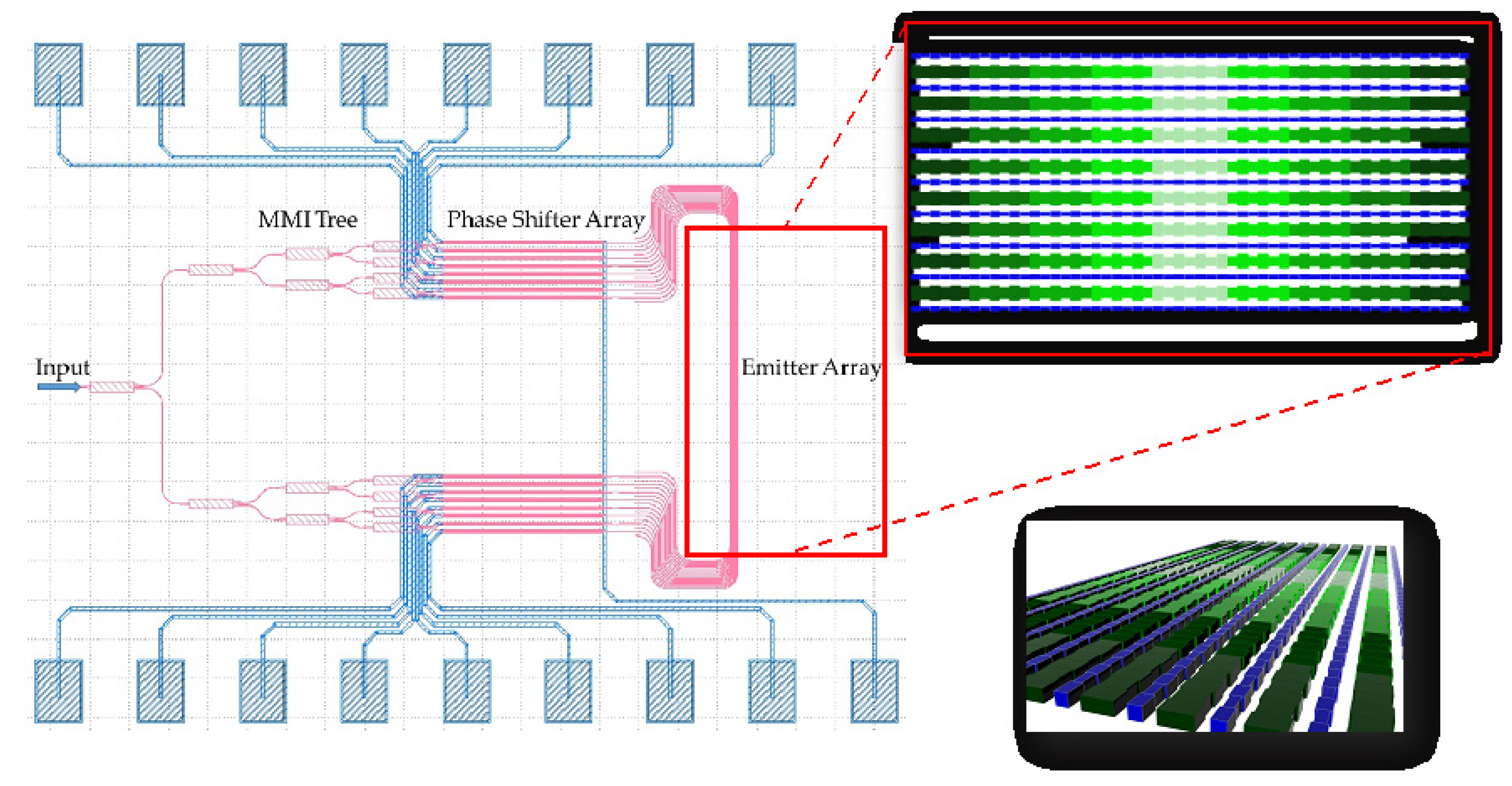
A two-dimensional dual-beam scanning grating array with varying waveguide line widths is shown in
Figure 1, of which the inset is for the 3-D schematic. Since the distance between the waveguide gratings is too small and prone to crosstalk, a passive grating microstructure is inserted through a smaller waveguide-width-based silicon ribbon (SR) grating array between the waveguide phase-shift. The finite element method (FEM) finds the best geometric parameters for the lowest crosstalk in the SR grating array. Then, the finite-difference time-domain (FDTD) method is executed to simulate the far-field pattern (FFP) and beam quality through the commercial software RSoft FullWAVE on a 32-channel SR grating array.
2. Theory and Design
For the dual-beam FBG structure, the transmission modes can be formed in the far- field to present two spots, where the effective refractive index
neff of the grating can be obtained by the effective mode theory and expressed as in the following Equation (1):
where
nI and
nE are the effective refractive indices of the silicon-on-insulator (SOI) waveguide in the non-etch and etch parts of the FBG, respectively.
F is the duty cycle of the grating structure and is chosen as 0.5 for easy processing in the linewidth consideration.
The distance between the antenna array is an essential parameter to design a large-angle beam scanning angle. The FoV is defined as the angle difference between the main and grating lobes, and the grating lobe angle Φ can be expressed in the following formula:
where
m is the diffraction order, Φ
m is the m-order angle of the grating lobe, Φ
0 is the main lobe angle, and
d is the waveguide grating spacing.
From the above Equation (2), it can be seen that when
d continues to increase, the angle difference between the main lobe and the first-order grating lobe will decrease, which means that the FoV reduces. Therefore, 600 nm is chosen as the grating spacing to get a large FoV although the crosstalk between the grating waveguides will increase. According to the coupling theory, when two geometrically identical waveguides transmit the same mode of light, it is easy to cause the two transmission modes to affect each other and cause a coupling phenomenon. Therefore, these two transmission modes are coupled entirely when their waveguide length reaches the coupling length [
12]. The following Equation (3) can express the coupling length
Lc between waveguides:
where
ns is the symmetrical mode,
na is the anti-symmetrical mode, and
λ is the incident light wavelength. The transmission mode can be regarded as two modes with the same amplitude: even and odd modes. Therefore, the effective refractive index difference will decrease through SR addition between the grating antenna, and the coupling length is enhanced to conduct the mutual crosstalk reduction.
In this study, the height of the transmitting silicon waveguide used in SOI is 220 nm, and the width is 500 nm. The center-to-center waveguide pitch of 550 nm is then utilized for a FEM coupling simulation through the effective refractive index difference between symmetric and asymmetric modes of the transmitting waveguides. The coupling length is theoretically derived to optimize the geometric parameters.
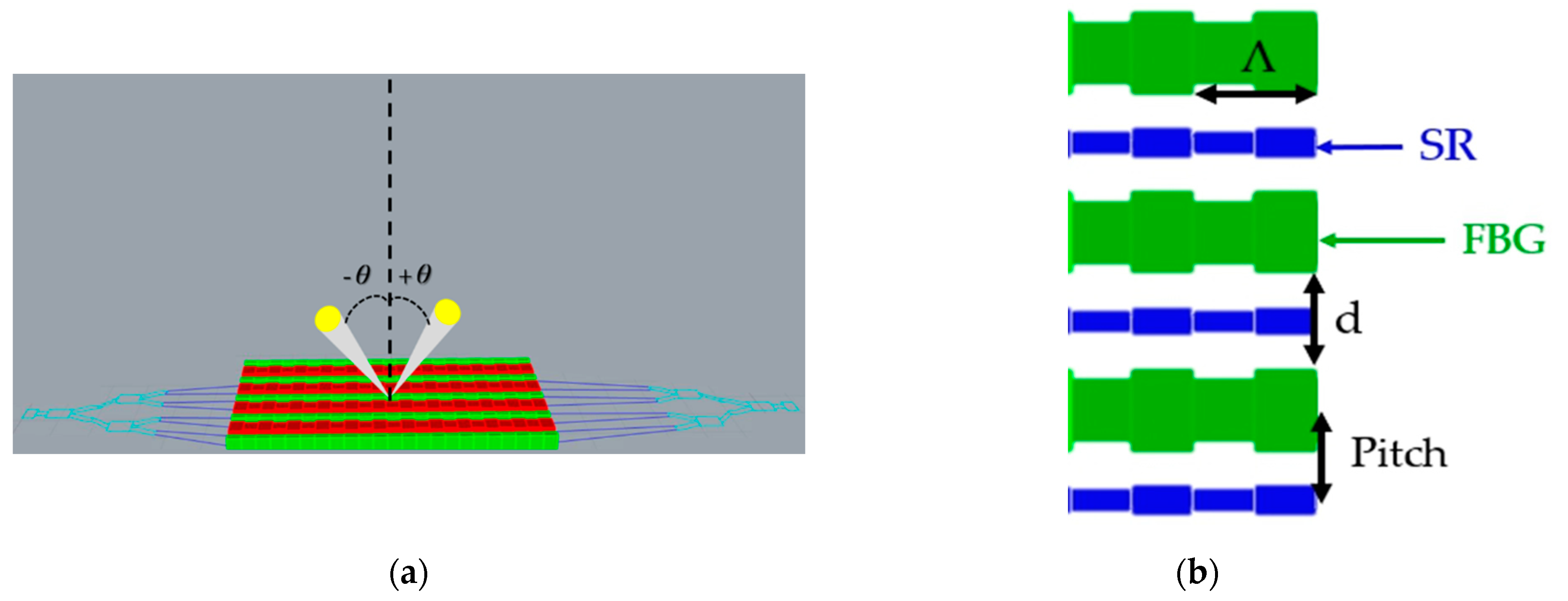
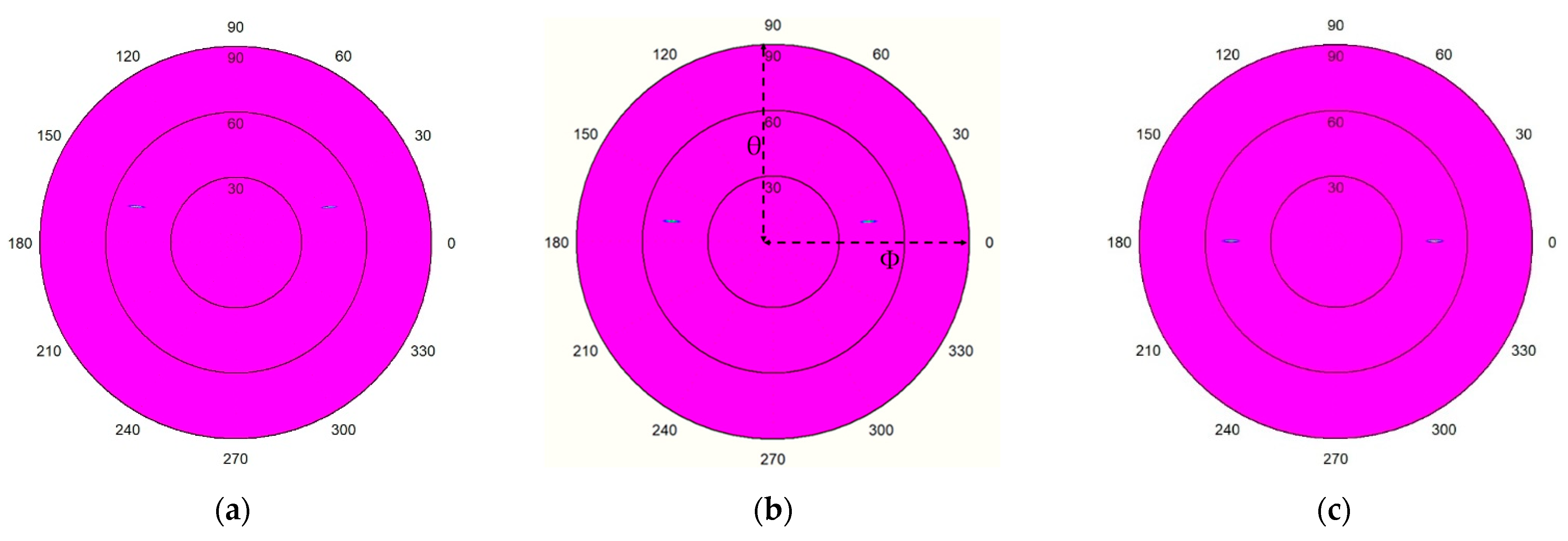
The effective refractive index of the FBG waveguide with different line width etching degrees was calculated by FEM after adding the silicon strip. The FBG with different line width combinations was designed by the effective refractive index and Bragg diffraction approaches. In this study, dual-beam scanning through bi-directional FBG was achieved by adjusting the wavelengths so that the light emitted from symmetrical angles can be scanned and can coincide at 0 degrees, as shown in
Figure 2a. The waveguide grating spacing, d, and the pitch between SR and FBG are demonstrated in
Figure 2b. The wavelength angle can be expressed by the following Equation (4):
where
nc is the cladding layer, generally for the air, equal to 1.
θ and
neff are the diffraction angle and effective grating index. Λ is the grating period length.
The available wavelengths of LiDAR operation are 1500 nm to 1600 nm. From the modulation through the center wavelength 1550 nm to long wavelengths and short wavelengths, the maximum rotation angle by the formula is about ±7~8 degrees [
13], which will be selected as the design target in this paper. For spot quality improvement after light emission, 20 grating cycles for each period of the chirped SR-based FBG will be utilized to calculate the energy loss through the energy decay theory. The particular decay constant can be expressed in the following Equation (5):
where
Pend is the residual light in the grating,
P0 is the energy of input light, α is the decay coefficient, and
z is the total grating length.
Linear radiation in the entire grating length is desired in OPA for good beam spot quality.
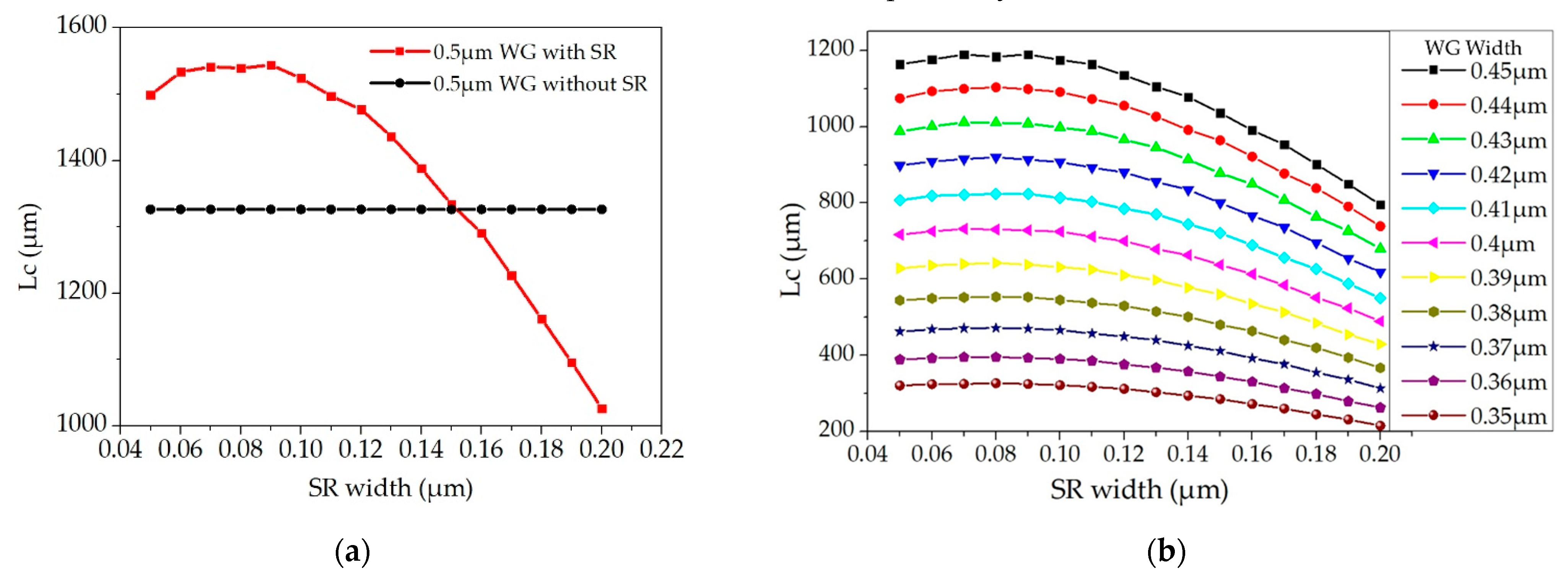
The inserted SR will enhance the coupling length [
12]. From Equation (3), the highest coupling length
LC is around 1575 μm when the SR width is between 90 nm and 100 nm for a 500 nm transmission waveguide width, as shown in
Figure 3a. The SR will cause more coupling, as its width is over 150 nm.
The transmission waveguide with a width lower than 350 nm experiences high optical loss for the non-steady mode and is selected to be between 350 nm and 450 nm for the coupling length optimization after the SR insertion. The following
Figure 3b shows the simulation results of the coupling length for various SR widths at the waveguide height of 220 nm under specific transmission waveguide widths. The coupling length is expected to be long to reduce the array crosstalk. The SR grating is inserted in the FBG as a blocking layer between the transmission waveguide array, and its narrow and wide widths are then selected as 90 nm and 100 nm, respectively.
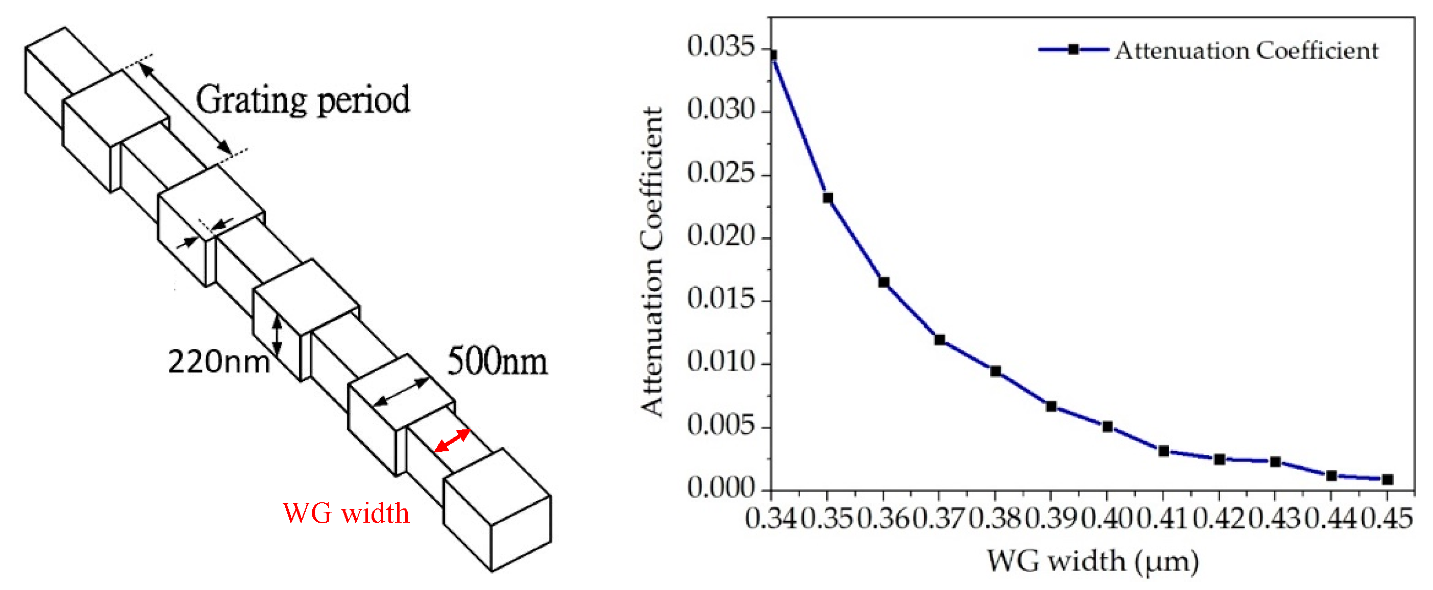
We used the FDTD to simulate 12 period FBG on various narrow grating waveguide widths at a fixed 500 nm wide width to calculate the attenuation coefficient, shown in
Figure 4. We can conclude that the significant refractive index variation will form stronger radiation with extensive waveguide width changes. Therefore, the light intensity decay in the single grating period length is intense, and the chirped FBG will be applied for the linear decay and steering emission in the FBG.
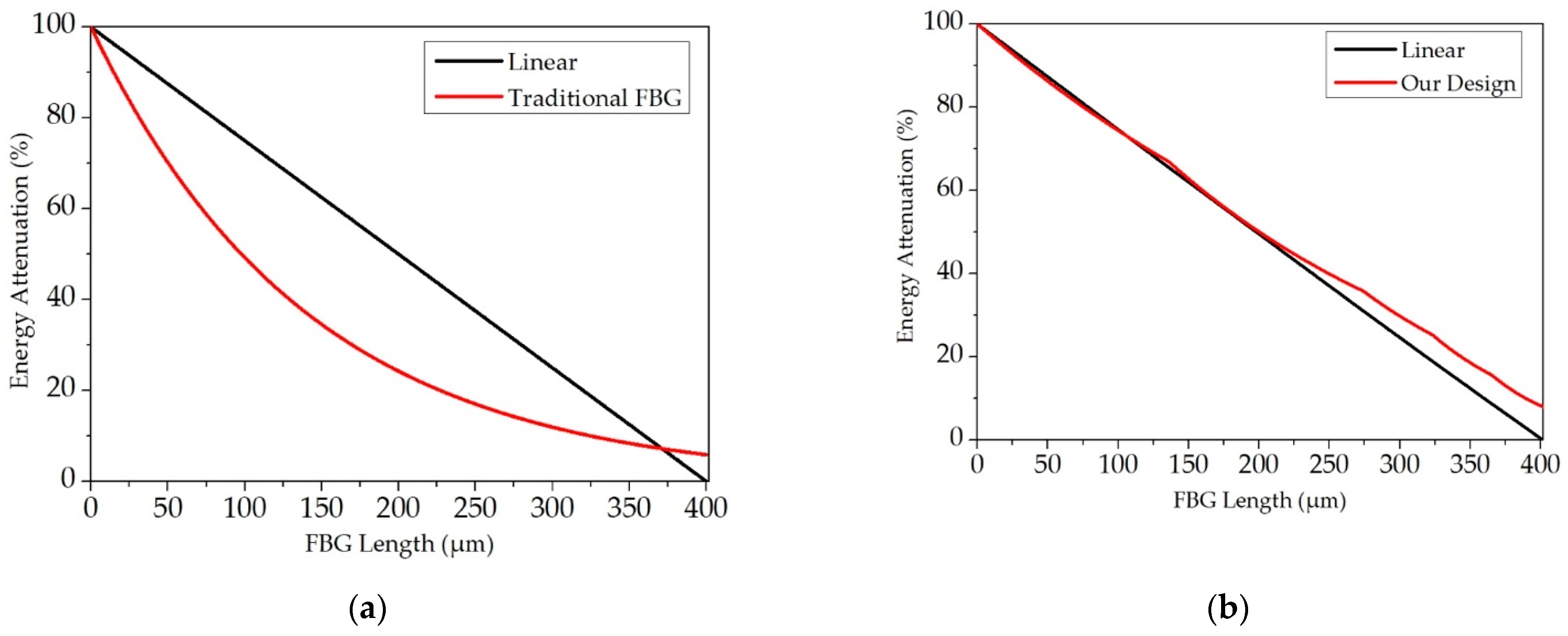
For a conventional single FBG, the most optical power beam radiation typically occurs before half of the effective length of the grating length. The power energy in the FBG behaves like 2nd or higher-order decay, as shown in
Figure 5a. However, the linear dissipation in FBG will form a dense beam spot because the total effective FBG length is proportional to the FWHM of the spectrum. Therefore, the chirped FBG array antenna is chosen and optimized for five periods to obtain the linear optical energy attenuation.
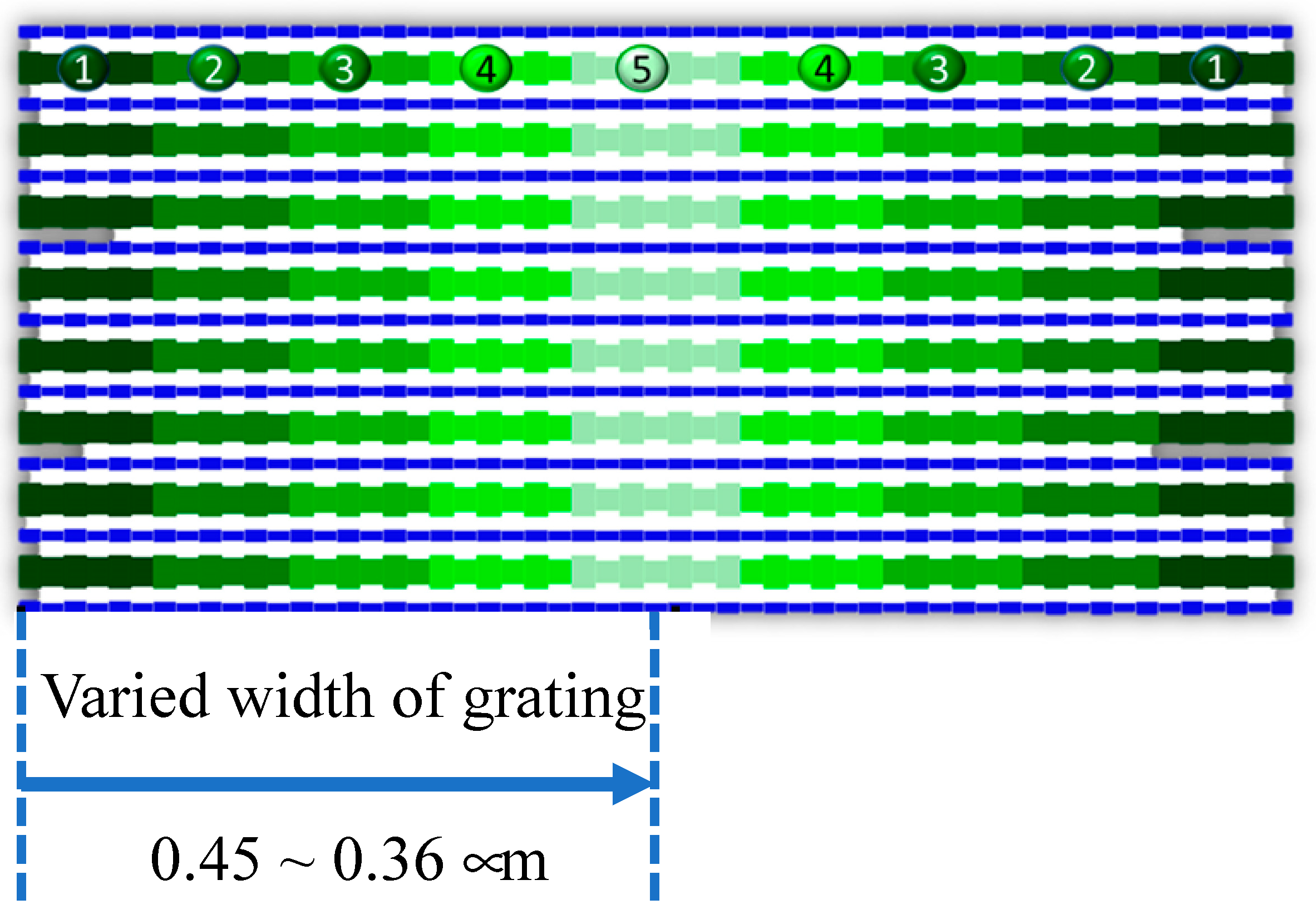
These 5 different waveguide widths ranging from 0.36 μm to 0.45 μm in a sequence of 0.45 μm, 0.42 μm, 0.4 μm, 0.38 μm, and 0.36 μm are selected for the narrowly chirped grating waveguide width and connected to a 500 nm wide transmission waveguide. Due to the lower attenuation coefficient of the higher narrow grating waveguide width, the period number in the 0.5–0.45 μm grating is higher than in the 0.5–0.36 μm grating, and the light transmission energy attenuation is shown in
Figure 5b. Through the total length of 767.2 μm in the FBG antenna, the bi-directional grating array will form a dual beam steering with linear optical power dissipation, as shown in
Figure 6. The related parameters are listed in
Table 1.
3. Results
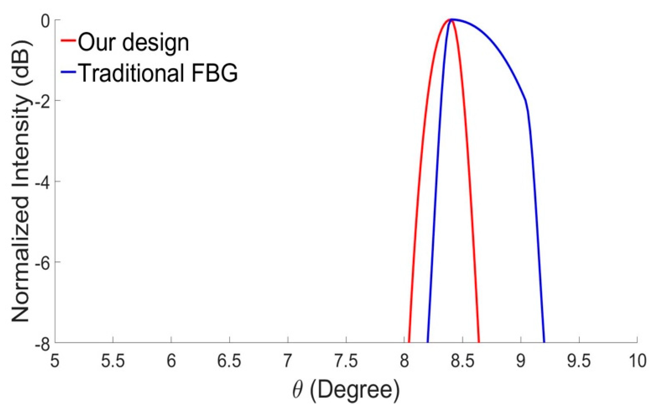
FDTD is used to calculate the FFP intensity of a 32-antenna-based bi-directional OPA, and the results in the center wavelength of 1550 nm for the traditional FBG are shown in
Figure 7a. The steering angle of the chirped FBG with SR appears at 8.4 degrees and is shown in
Figure 7b. Due to the linear radiation through the whole physical grating length, the 0.24 degrees of FWHM in the theta direction from the SR-based chirped FBG is better than 0.82 degrees via the conventional FBG, as shown in
Figure 8.
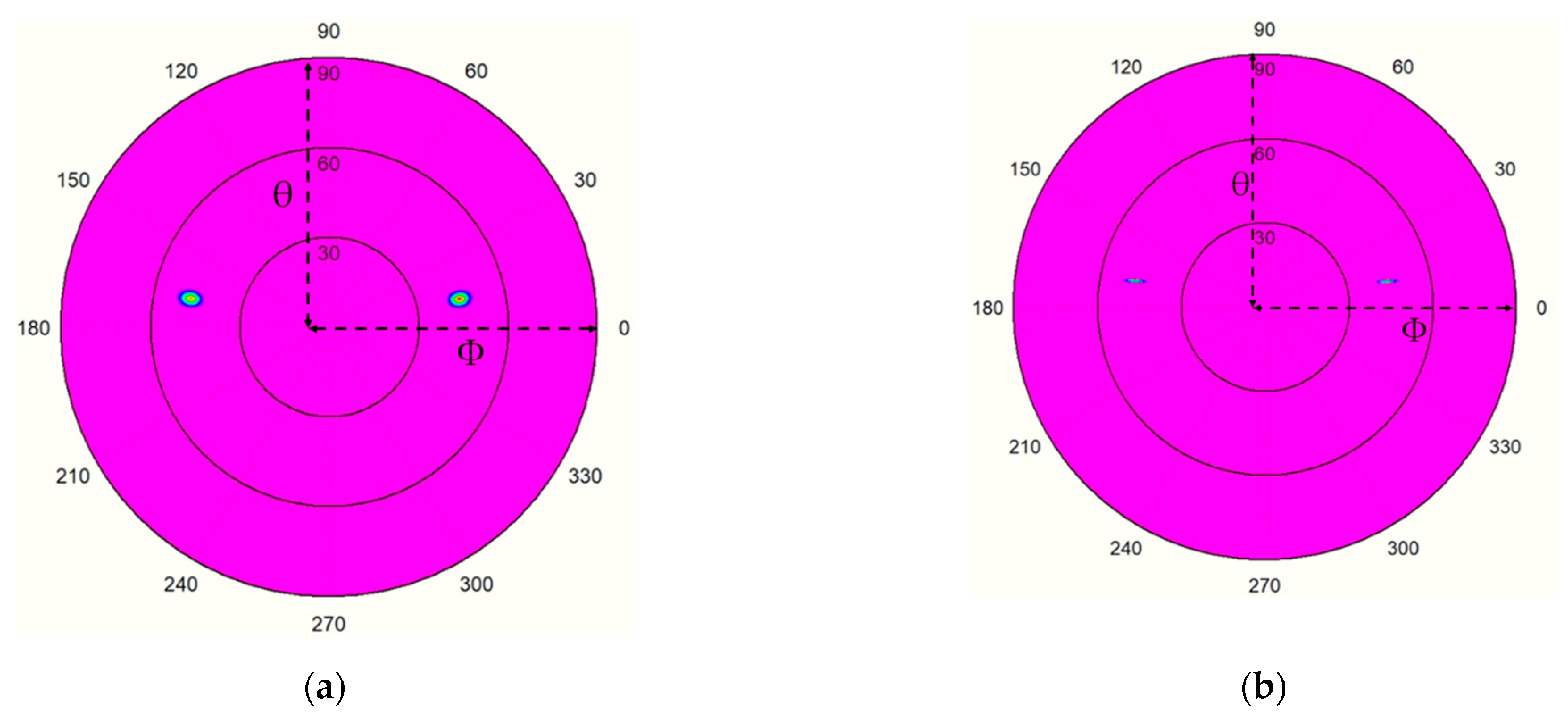
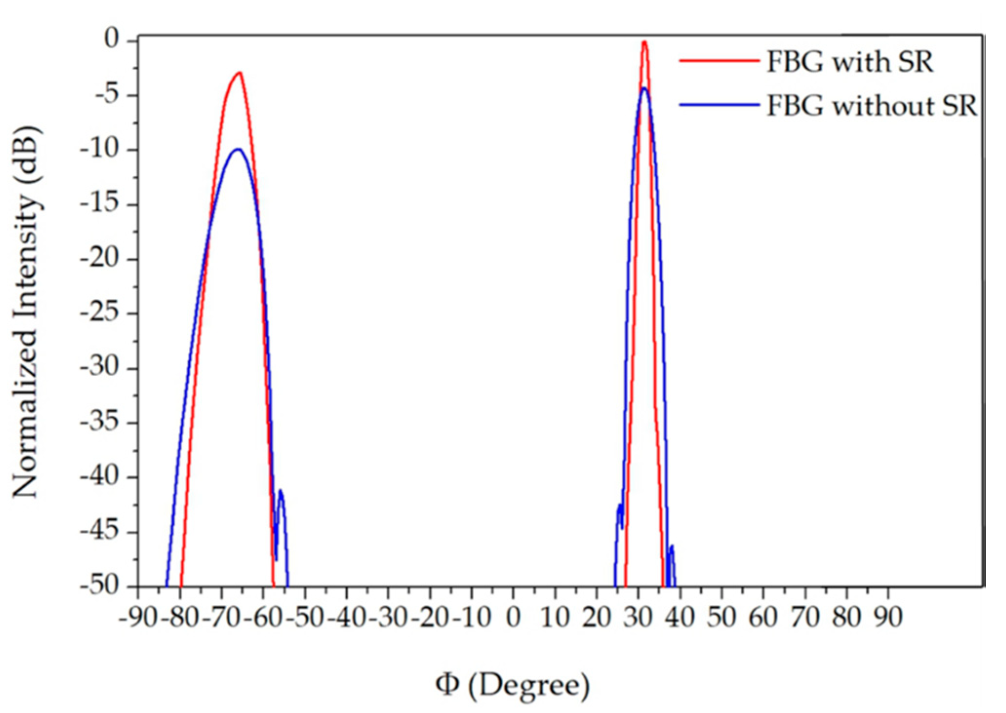
After the 0.167π phase difference of each of the 32 antennas is applied, the FFP main beam of the chirped FBG OPA with SR through FDTD demonstrates 30 degrees in the Φ horizontal directions, and the grating lobe is −65 degrees. Therefore, an FoV with the SR inserted in the 0.6 μm pacing FBG could reach 95 degrees in the Φ direction, as shown in
Figure 9. The side lobe adjacent to the main and grating lobes of the FBG in this study is reduced by about 10 dB. The reduced energy was concentrated on the main lobe and the grating lobe, resulting in a 6 dB increase in the total spot energy intensity.
In this bi-directional OPA, the light will be injected into the phased array through two sets of the grating antennas by the equal path-length S-bend. The wavelength adjustment from 1510 nm to 1600 nm can move a spot from 15 degrees to −0.8 degrees in the theta direction, and the total moving angle is about 15.8 degrees, as shown in
Figure 10. The steering angle of the 1500 nm center wavelength is ±15 degrees in the theta direction through two sets of inputs, as shown in
Figure 11a, and the 1550 nm wavelength moves to ±8.4 degrees, as shown in
Figure 11b. A total shift of ∓0.8 degrees is observed at the 1600 nm wavelength. The beam steering for bi-directional grating antennas of the SR-based chirped FBG OPA demonstrates that the θ horizontal directions have a FoV of 30 degrees.
Table 2 shows the comparison between the 32-channel low-coupled dual-beam linear attenuator antenna designed in this study and recent OPA designs [
14,
15,
16,
17]. The emitter number of each OPA is shown in the fourth column. The linear attenuator design in this study achieves a similar FWHM in the theta direction at a 400 μm length compared with some OPAs using longer grating antennas. When the grating spacing is reduced to 600 nm, the last column shows that the steering angles in the vertical and horizontal direction can be demonstrated to be 95 and 30 degrees, respectively. The 30 degrees in the vertical beam steering is to modulate the 90 nm bandwidth from 1510 to 1600 nm wavelength in this kind of SR-grating-based bi-directional chirped FBG.
4. Summary and Discussion
We propose an OPA structure built on an SOI chip using a waveguide array with varying line widths below the half-wavelength spacing. An SR grating array is then implemented between the chirped FBG emitting arrays for crosstalk reduction. Finally, the OPA with bi-directional emitters demonstrates a large FoV and low crosstalk.
The FDTD is used to simulate a 32-channel OPA by adding an SR grating array between grating antennas at a distance of 600 nm. The mutual phase effect is diminished and effectively increases the OPA FoV in the Φ direction to 95 degrees. The crosstalk reduction also reduces the side lobe of the spot by about 10 dB and makes the beam more focused, increasing the overall beam intensity by 6 dB. This study also demonstrates various fishbone grating line widths to form linear optical-power radiation to cause the effective length of the grating antenna to approximate the physical size. The FWHM in the theta vertical direction can be reduced and reaches about 0.24 degrees. The OPA can be directed to two input grating antennas for two spots in the θ direction for this symmetric grating design. Then, by adjusting the input wavelength from 1510 nm to 1600 nm, the FoV in the θ direction can achieve 30 degrees. In the future, the chirped FBG built with SR grating in the wavelengths from 1450 nm to 1600 nm can be designed to improve the steering angle further and increase the antenna channel number to reduce the FWHM in the Φ direction more effectively.
The advantages of the single beam system are its simple construction and ease of operation in phase control. Its disadvantages are its small FoV. On the other hand, the benefit of the dual-beam system is its large FoV, which is almost two times larger than a single beam. Its disadvantages are the complicated phase control and an additional optical switch, which will steer the dual beams in sequence for free interference.
The dual vertical beams pass through the antenna array of a bi-directional fishbone grating, and the zero-degree top light steers to ±θ angles, respectively, for emitting. Since there is no crossing steer angle, an optical switch will be implemented to allow steering for only one side angle beam for reflection distinguishment and free interference.


