Article

Surface Passivation of Crystalline Silicon Wafer Using H2S Gas

1
Department of Electrical and Computer Engineering, Sungkyunkwan University, Suwon 16419, Korea
2
Smart Energy & Nano R&D Group, Korea Institute of Industrial Technology, Gwangju 61012, Korea
*
Author to whom correspondence should be addressed.
Appl. Sci. 2021, 11(8), 3527; https://doi.org/10.3390/app11083527
Submission received: 25 March 2021 / Revised: 12 April 2021 / Accepted: 12 April 2021 / Published: 15 April 2021
(This article belongs to the Special Issue Applications of Nano-Electronic Devices)

Abstract

:
We report the effects of H2S passivation on the effective minority carrier lifetime of crystalline silicon (c-Si) wafers. c-Si wafers were thermally annealed under an H2S atmosphere at various temperatures. The initial minority carrier lifetime (6.97 μs) of a c-Si wafer without any passivation treatments was also measured for comparison. The highest minority carrier lifetime gain of 2030% was observed at an annealing temperature of 600 °C. The X-ray photoelectron spectroscopy analysis revealed that S atoms were bonded to Si atoms after H2S annealing treatment. This indicates that the increase in minority carrier lifetime originating from the effect of sulfur passivation on the silicon wafer surface involves dangling bonds.

Graphical Abstract

1. Introduction

In recent years, photovoltaic systems are becoming very popular because of their enormous amount of clean and unlimited solar energy, which can be harvested through photovoltaic solar cells [1,2,3]. Among the various technologies that increase solar cells’ efficiency, surface passivation treatment plays a key role in the silicon-based solar cell fabrication process. The dangling bonds on the silicon wafer surface are known to work as recombination centers and cause the loss of photon-generated carriers. Many advanced passivation materials have been developed and are widely used in commercial production, including SiNX:H, SiOX, and AlOX [4,5,6,7,8,9]. These materials have been shown to have good passivation effects on the silicon wafer surface. However, these materials are produced through complex fabrication systems that necessitate precise control of gaseous reactants [10].
According to Mead and Spitzer, the high density of the semiconductor/metal interface will pin the interfacial Fermi level, making the barrier height less sensitive to the metalwork function [11]. Experimentally, Ali found that sulfur-passivated silicon substrates show greater sensitivity to the metalwork function in terms of Schottky barrier height [12]. This was attributed to the reduction in surface density through passivation of dangling silicon bonds by S. Previous results show that S atoms are absorbed on the Si wafer surface in the form of Si–S–Si bridge bonds [13,14]. The significant minority carrier lifetime gains of multicrystalline Si recently achieved by sulfur treatment further prove that sulfur treatment can effectively passivate dangling silicon bonds on the surface [15].
In this study, we report the effect of sulfur passivation on crystalline silicon wafers using H2S annealing treatment at various temperatures. The results show that a significant improvement in passivation can be obtained after H2S annealing treatment. Moreover, 600 °C was found to be the best temperature condition for crystalline silicon wafers. Under this condition, the highest minority carrier lifetime gain of up to 2030% can be observed using the Sinton WCT-120 measurement system.

2. Materials and Methods

N-type flat c-silicon wafers (100) with 1–10 ohm·cm, 200 μm were used for the experiments. Before the experiments, the wafers were cleaned in a 3-step process: saw damage removal, organic cleaning, and ionic cleaning. For saw damage removal, the wafers were soaked in 45% KOH solution at 70 °C for 20 min. For organic and ionic cleaning, the wafers were cleaned in standard RCA-1 and RCA-2 procedures in sequence [16,17]. After cleaning, the oxide layer induced by H2O2 was removed by 1% HF for 30 s. Afterward, the silicon wafers were blow-dried quickly to prevent reoxidation.
H2S annealing treatments were conducted in a 2-zone quartz tube furnace. The quartz tube was pumped to a pressure of 5 mTorr before being charged with H2S gas. To thoroughly evacuate the air from the quartz tube, the tube was charged with H2S gas twice before annealing treatment was begun. Then, the quartz tube was heated to the desired temperature. The annealing processing time was 20 min. When the processing time ran out, the H2S gas was pumped out of the tube, and the heater was turned off. During the cooling time, argon gas was introduced into the tube at a flow rate of 20 sccm. The silicon wafers were unloaded when the temperature dropped below 50 °C. For reproducibility, each condition was tested three times, and the average value was taken, as shown in Figure 1 and Table 1.
The surface morphology of the CuI films was characterized using a scanning electron microscope (JSM-7610F, JEOL, Tokyo, Japan). The surface reactions were monitored by transmission-mode Fourier-transform infrared (FTIR) spectroscopy. The composition of the silicon wafers was analyzed using XPS (k-alpha, Thermo Fisher Scientific, Waltham, MA, USA). Lifetime measurements were done with a WCT-120 lifetime tester from Sinton instruments.

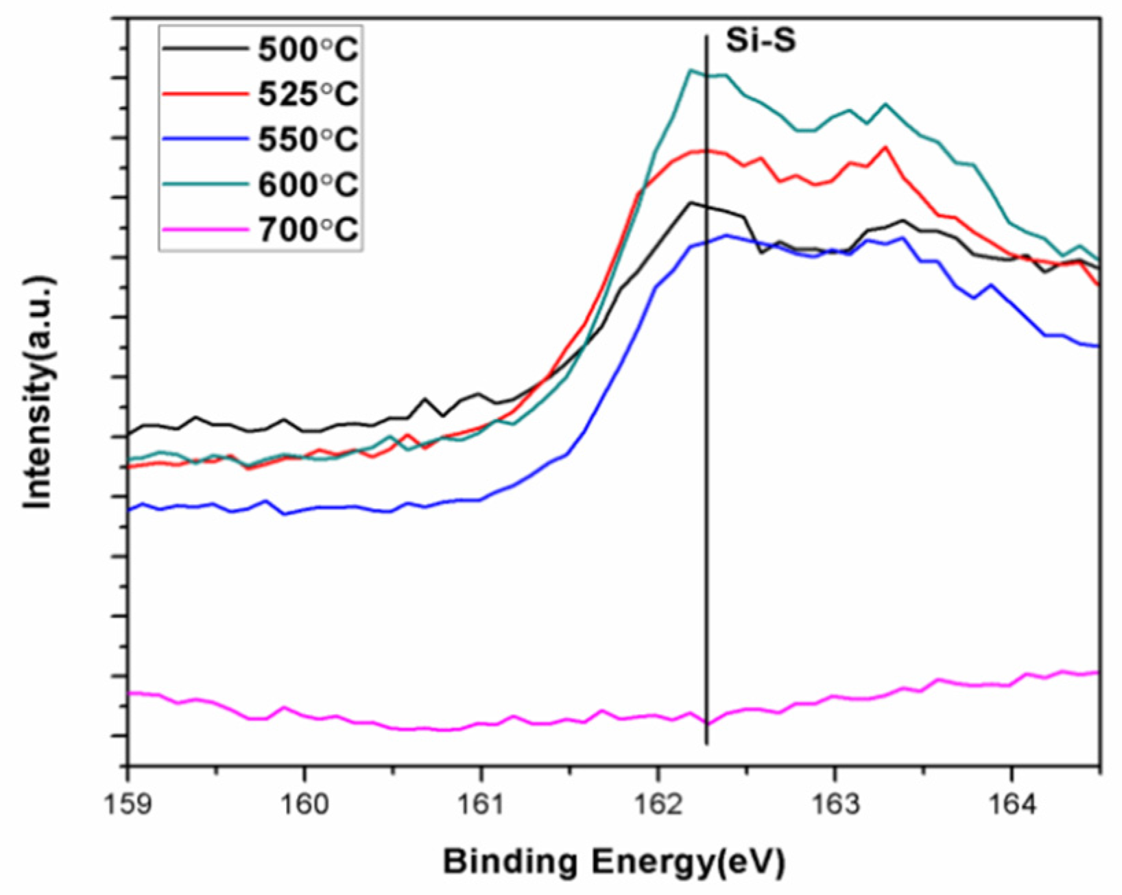
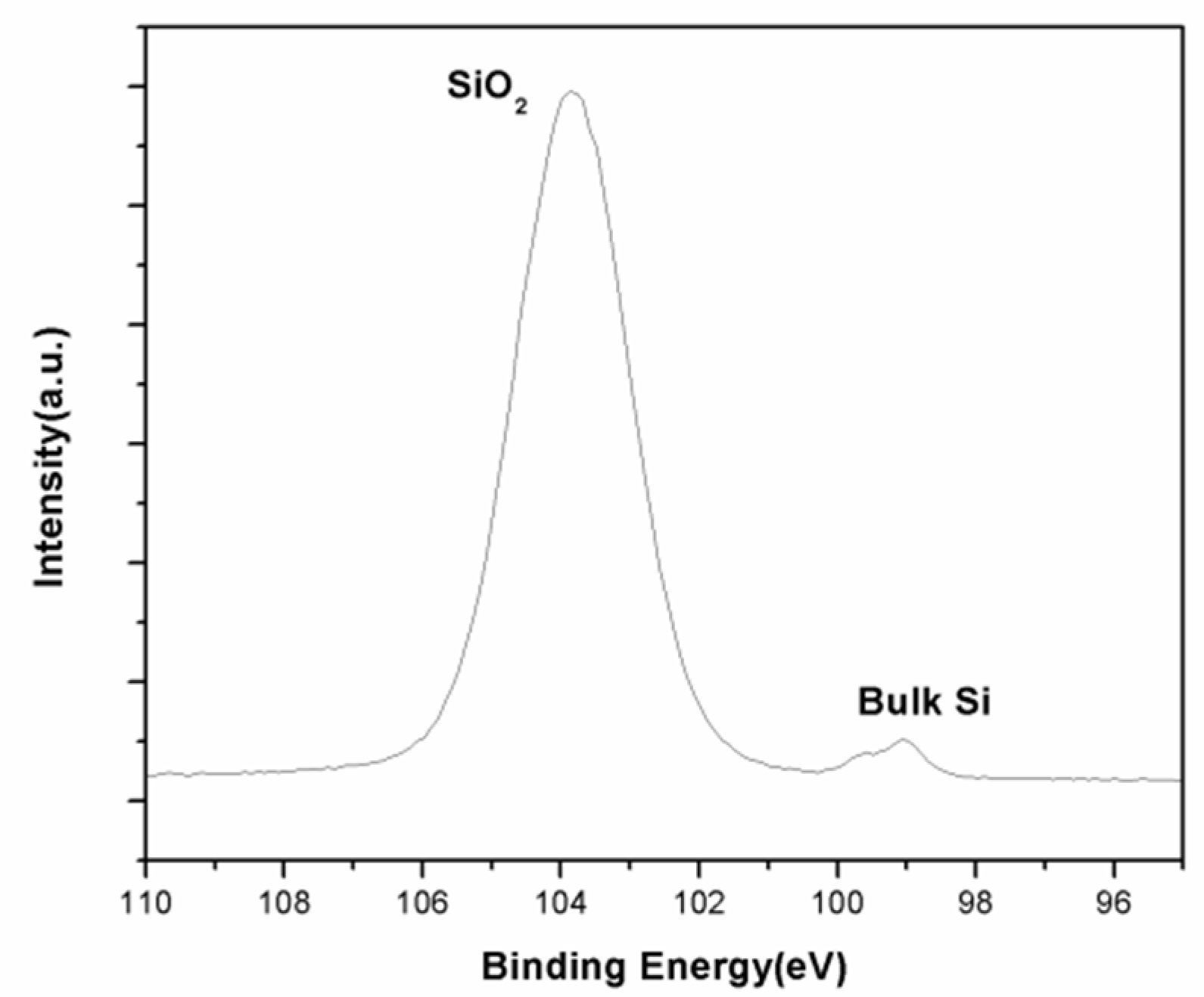
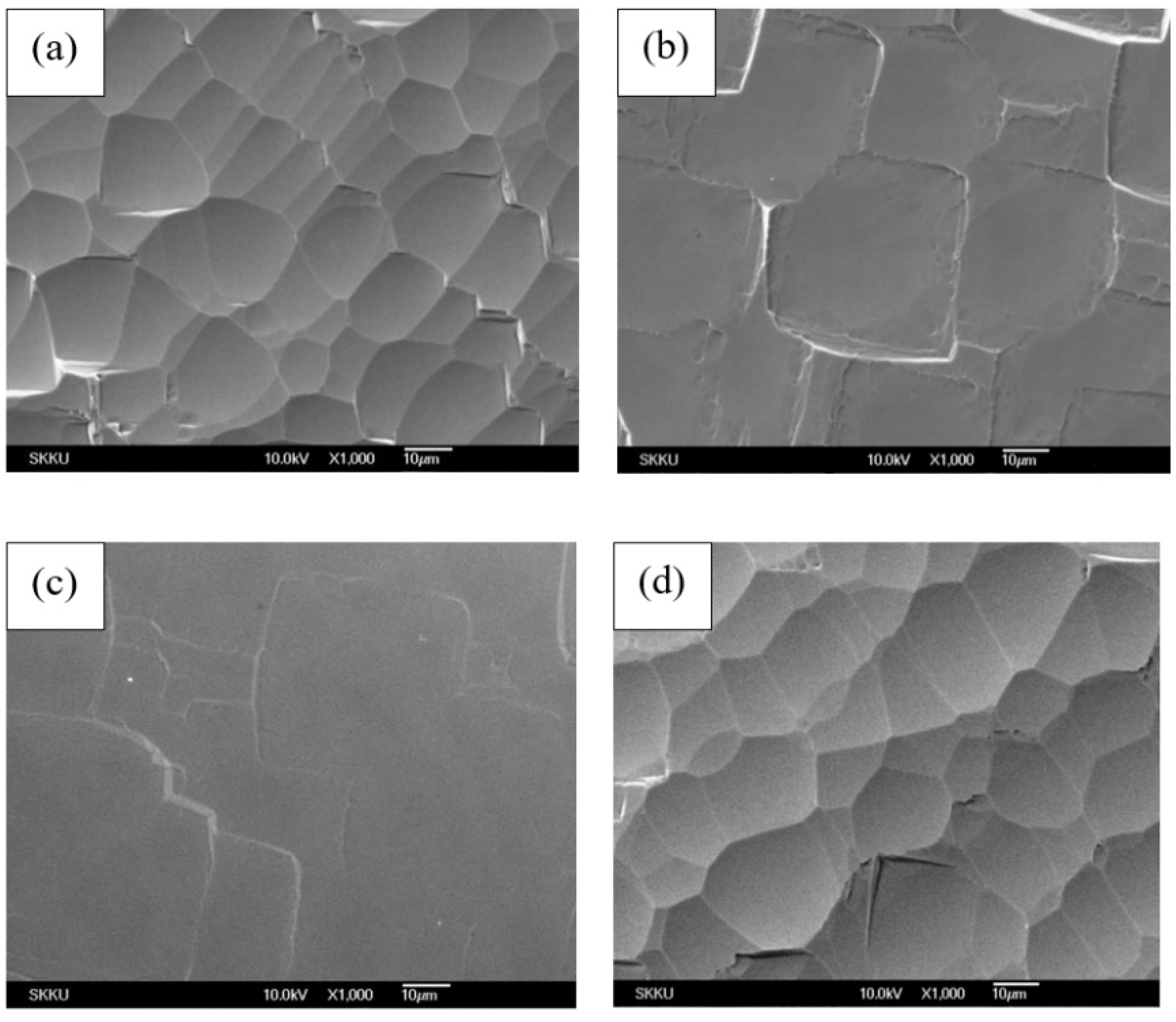
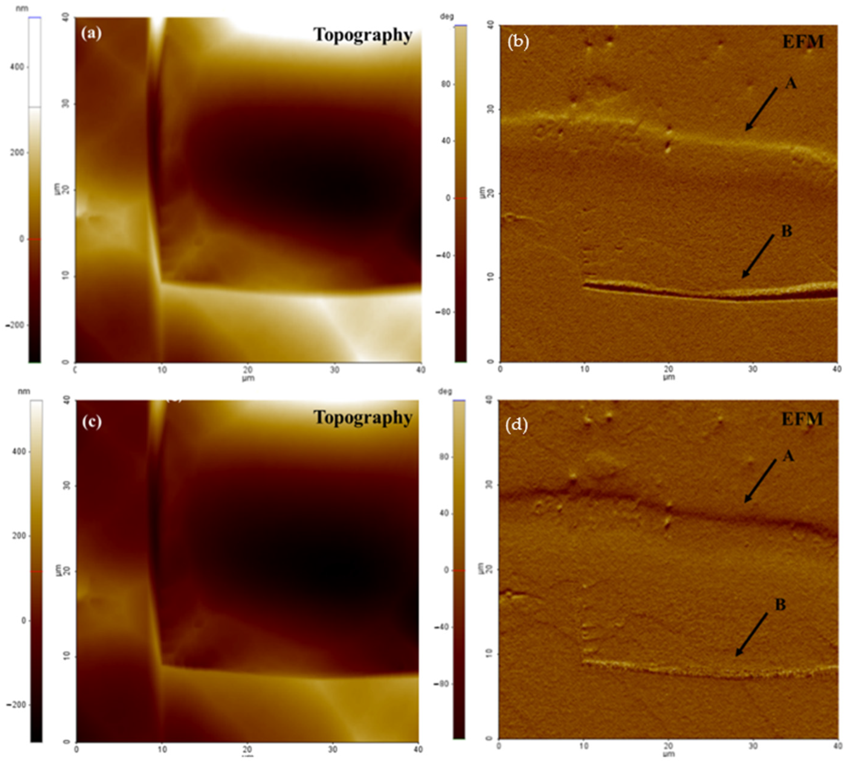
3. Results and Discussion

Passivation quality was measured with a Sinton WCT-120 instrument. It is widely known that silicon wafers show huge fluctuations in minority carrier lifetime. Due to wafer quality fluctuations, the gain in minority carrier lifetime is used to represent passivation quality. After the wafer cleaning procedure, H2S annealing experiments were carried out to investigate the relationship between temperature and passivation quality. Figure 1 and Table 1 show the minority carrier lifetime gain vs. temperature. In this minority carrier lifetime gain-temperature plot, 2 peaks were observed; one is 1610% at 525 °C, and the other one is 2030% at 600 °C. Yinghuang found that H2 is the desorption product of thermal decomposition of H2S on silicon [9]. Later, Arunodoy experimentally proved that passivation quality on silicon is related to the combined effect of hydrogen and sulfur atoms [14]. Hence, the 2 peaks in the table probably stem from the same passivation mechanism as reported by Arunodoy. Compared with the highest minority carrier lifetime gain (2750%) obtained by Arunodoy, the H2S passivation quality seems inferior. However, it should be noted that minority carrier lifetime gain is strongly related to the silicon wafer properties itself. Specifically, the differences in material properties between the monocrystalline silicon wafer and the multicrystalline silicon wafer used in the previous case most likely resulted in the different upper limits of minority carrier lifetime gain. A large number of bulk defects are known to exist along the grain boundaries in multicrystalline silicon [18,19]. However, in monocrystalline silicon, the absence of grain boundaries means that these kinds of bulk defects are practically negligible. In other words, monocrystalline silicon is superior to multicrystalline silicon in terms of bulk defects. This is also proven by the low initial minority carrier lifetime of multicrystalline vs. monocrystalline silicon. Hence, a more profound gain in minority carrier lifetime can be obtained on multicrystalline silicon by the same method. Moreover, a strange phenomenon was observed: the minority carrier lifetime gain increased again when the annealing temperature was higher than 650 °C. To elucidate this phenomenon, XPS characterization was used to analyze silicon surface composition and further investigate the passivation mechanism. Figure 2 shows the S 2p XPS spectra for the H2S-passivated Si surface. Most conditions exhibit peaks at 162.3 eV, corresponding to Si–S bonds [20]. At 500, 525, 550, and 600 °C, the peaks’ intensity exhibits the same tendency as the minority carrier lifetime gain when the annealing temperature increases from 500 °C to 600 °C. For example, the highest and second-highest peak perfectly corresponds to the largest and second-largest minority carrier lifetime gain. This means that sulfur plays a dominant role in passivation performance. However, it seems that the 550 °C condition does not follow this trend. It exhibits a lower Si–S peak intensity than that seen at 500 °C, but a larger minority lifetime gain. Both hydrogen and sulfur are believed to play important roles in passivation performance. Thus, it is possible that the more positive passivation effect of hydrogen compensates for the loss of sulfur and enhances the total passivation performance to a higher level than that seen under 500 °C conditions. However, there is no peak at 162.3 eV at 700 °C, meaning that no Si–S bonds form on the Si surface after 700 °C H2S annealing treatment. However, a high minority carrier lifetime gain was observed in reality, which contradicted the conclusion that sulfur plays a dominant role in passivation performance. The answer to this conundrum can be found in Figure 3. The peaks at 103.8 and 99.1 eV correspond to SiO2 and Si, respectively [21]. From Figure 3, it is clear that the SiO2 peak is much higher than the Si bulk peak.
This means that the silicon wafer was thoroughly covered by SiO2. It explains why the passivation performance was still good when there was no sulfur bonded with silicon dangling bonds. It also coincides with previous research showing that sulfur atoms will desorb at high temperatures [22]. Thermal oxidation for silicon oxide growth is widely used in laboratory or industrial production. Here, the 2-zone furnace provided a similar environment. Even though the experiment was conducted in a vacuum environment, a tiny amount of O2 cannot be evacuated from the furnace. Because surface dangling bonds were not terminated by sulfur, the bare silicon surface is more positive and sensitive to O2, especially under high-temperature conditions. In the next section, the effects of various annealing temperatures on the wafers’ morphology will be discussed. Figure 4 shows SEM images of silicon wafers after H2S annealing treatment. In this study, the wafers (100) were processed with saw damage etching by KOH solution. Figure 4a shows an SEM image of a Si wafer without H2S annealing treatment. Many square shapes were formed on the wafer surface, which is caused by isotropic etching [23,24]. Previous research showed that H2S treatment would result in the formation of a thin sulfur layer on Si or Ge substrates [20]. The morphology shown in Figure 4b,c is obviously different from that shown in Figure 4a. The silicon surface was covered with a thin layer after 525 °C H2S annealing treatment, as shown in Figure 4b. The identity of this layer was confirmed to be sulfur by the above-mentioned XPS spectra and EDX mapping results. In Figure 4b, the wafer surface is flat, and the boundaries between the square shapes are difficult to distinguish, which can be attributed to the increased thickness of the sulfur film. It can be further concluded that the thin sulfur layer becomes thicker under the higher annealing temperature of 600 °C, which is consistent with the intensities of the XPS peaks. Based on the above discussion of the XPS spectra, we concluded that the passivation performance reflects the amount of sulfur. Here, the SEM findings show the same result, that passivation performance is related to the amount of surface sulfur. The sulfur thin layer becomes rough again under 700 °C annealing treatment, as shown in Figure 4d. This finding is following XPS results showing that there are no sulfur atoms on the silicon surface when the annealing temperature is raised to 700 °C or higher. Silicon-based solar cell passivation performance mainly stems from two factors: termination of surface dangling bonds and rejection of the minority carrier due to the field effect. Herein, the potential second passivation theory was investigated. Electrostatic force microscopy (EFM) is a very useful technique to investigate surface charge-related phenomena, such as the surface field so, EFM was used to measure the silicon wafer surface, as shown in Figure 5. The existence of a fixed charge in SiNx and BSF (Al contact) is known to bring pretty good passivation performance to commercial solar cells [25,26,27]. Hence, we suspect that the cause must be related to the surface charge if the possibility of dangling bond termination was denied. The detection and distribution of a surface charge on silicon were first investigated by Morita [28]. The response of surface charge to bias voltage is believed to result in differences in the topography or EFM images. Before measurements were taken, aluminum contact was deposited on half of the samples’ area for comparison purposes. Then, forward bias voltage (5 V) was applied to the samples first, and reverse bias voltage (−5 V) was applied second. The measurement area was defined as 40 μm2. According to previous research, the appearance of new patterns and color changes in the same area would strongly indicate the existence of a surface charge. It should be noted that the color changes of lines A and B come from the height difference. They were caused by Al contact and chemical solution etching (saw damage removal), respectively. Hence, it can be concluded that no surface charge exists on the silicon wafer surface.

4. Conclusions

In this study, the passivation effect of H2S gas annealing on silicon wafers was investigated, and the optimal annealing temperature was 600 °C. The XPS spectra study shows the passivation performance reflects the amount of sulfur, and the SEM analysis also shows that passivation performance is related to the amount of surface sulfur, while the possibility of surface charge passivation was excluded by EFM. This research shows that the amount of sulfur plays a dominant role in the passivation performance and that all sulfur will thoroughly disappear from the silicon surface when the temperature is increased to 700 °C. These findings show that sulfur passivation is an excellent candidate for a simple and economical passivation method. For further work, this technology will be applied to photovoltaic devices for making high-efficiency solar cells.

Author Contributions

Conceiving the idea, J.L. (Jaehyeong Lee), J.Y. (Junsin Yi), C.J., J.L. (Jian Lin); designing the study, J.L. (Jian Lin), H.J., J.Y. (Junsin Yi); experiments, J.L. (Jian Lin), J.Y. (Junsin Yi); data analysis, J.L. (Jian Lin), H.J.; writing—original draft, J.L. (Jian Lin), J.L. (Jaehyeong Lee), writing—review and editing, H.J., J.L. (Jaehyeong Lee); supervision, J.L. (Jaehyeong Lee). All authors have read and agreed to the published version of the manuscript.

Funding

This study was supported by the Korea Electric Power Corporation (Grant number: R17XA05-1).

Data Availability Statement

The data that support the findings of this study are available from the corresponding author, J.L., upon reasonable request.

Conflicts of Interest

The authors declare no conflict of interest.

References

  1. Hongsub, J.; Jinho, S.; Daehan, M.; Jaehyeong, L.; Chaehwan, J. Improvement in power of shingled solar cells for photo-voltaic module. J. Nanosci. Nanotechnol. 2020, 20, 7096–7099. [Google Scholar]
  2. Ajitha, A.; Nallapaneni, M.K.; Xiao, J.; Guduru, R.R.; Arunkumar, J.; Kadapalla, P.; Anil, K. Underwater performance of thin-film photovoltaic module immersed in shallow and deep waters along with possible applications. Results Phys. 2019, 15, 102768. [Google Scholar] [CrossRef]
  3. Pramod, R.; Maria, M.; Nallapaneni, M.K.; Sastry, O.S.; Arunkumar, J. Operational performance and degradation influenced life cycle environmental-economic metrics of mc-Si, a-Si and HIT photovoltaic arrays in hot semi-arid climates. Sustainability 2020, 12, 1075. [Google Scholar] [CrossRef] [Green Version]
  4. Anton, E.; Christian, R.; Armin, R.; Jan, B. Influence of layer thickness on passivation properties in SiOx/Al2O3 stacks. J. Appl. 2020, 127, 235303. [Google Scholar]
  5. Teng, C.K.; Kean, C.F.; Matthew, S.; Keith, M.; Evan, F.; Sieu, P.P.; Wensheng, L.; Andrew, B. Excellent ONO passivation on phosphorus and boron diffusion demonstrating a 25% efficient IBC solar cell. Prog. Photovolt. 2020, 28, 1034–1044. [Google Scholar]
  6. Kai-Yuan, C.; Shang-Chi, W.; Chia-Jui, Y.; Tong-Wen, W.; Jyun-Hao, L.; Meng-Chyi, W. Comparative study on performance of AlGaN/GaN MS-HEMTs with SiNx, SiOx, and SiNO surface passivation. Solid State Electron. 2020, 170, 107824. [Google Scholar]
  7. Mickael, L.; Shota, N.; Hitoshi, S.; Koji, M. Passivation property of ultrathin SiOx:H/a-Si:H stack layers for solar cell applications. Sol. Energy Mater. Sol. Cells 2018, 185, 8–15. [Google Scholar]
  8. Armin, G.A. Surface passivation of crystalline silicon solar cells: A review. Prog. Photovolt. 2000, 8, 473–487. [Google Scholar]
  9. Mohammad, Z.R.; Shahidul, I.K. Advances in surface passivation of c-Si solar cells. Mater. Renew. Sustain. Energy 2012, 1, 1–11. [Google Scholar]
  10. Zongjie, S.; Yanfei, Q.; Ivona, Z.M.; Cezhou, Z.; Steve, H.; Li, Y.; Tian, L.; Yanbo, H.; Chun, Z. Effect of annealing temperature for Ni/AlOx/Pt RRAM devices fabricated with solution-based dielectric. Micromachines 2019, 10, 446. [Google Scholar]
  11. Mead, C.; Spitzer, W.G. Fermi level position at metal-semiconductor interfaces. Phys. Rev. 1964, 134, A713–A716. [Google Scholar] [CrossRef] [Green Version]
  12. Muhammad, Y.A.; Meng, T. Effect of sulfur passivation of silicon (100) on Schottky barrier height: Surface states versus surface dipole. J. Appl. 2007, 101, 103708–1–103708–5. [Google Scholar]
  13. Ying-Huang, L.; Chuin-Tih, Y.; Yi-Hsin, L.; Wei-Hsiu, H. Adsorption and thermal decomposition of H2S on Si(100). Surf. Sci. 2002, 519, 150–156. [Google Scholar]
  14. Qifei, W.; Boris, V.Y.; Theodore, E.M. Adsorption and decomposition of H2S on UO2(001). Surf. Sci. 2003, 523, 1–11. [Google Scholar]
  15. Arunodoy, S.; Haifeng, Z.; Wen-Cheng, S.; Meng, T. A new method for bulk passivation in multicrystalline-Si by sulfur. In Proceedings of the IEEE 42nd Photovoltaic Specialist Conference (PVSC), New Orleans, LA, USA, 14–19 June 2015. [Google Scholar]
  16. John, V. Thin Film Processes, 1st ed.; Academic Press: Cambridge, MA, USA, 1978. [Google Scholar]
  17. Werner, K. Handbook of Semiconductor Cleaning Technology; Noyes Publishing: Park Ridge, NJ, USA, 1993. [Google Scholar]
  18. Jerry, G.F.; Fredrik, A.L. Theory of grain-boundary and intragrain recombination currents in polysilicon p-n-junction solar cells. IEEE Trans. Electron Devices 1980, 27, 692–700. [Google Scholar]
  19. Amal, K.G.; Charles, F.; Tom, F. Theory of the electrical and photovoltaic properties of polycrystalline silicon. J. Appl. 2008, 51, 446–454. [Google Scholar]
  20. Tae, J.S.; Young, J.C.; Hyun, S.J.; Dae, H.K.; Dae, W.K.; Sang-Moon, L.; Jong-Bong, P.; Jung-Yeon, W.; Seong, K.K.; Cheol, S.H.; et al. High quality interfacial sulfur passivation via H2S pre-deposition annealing for an atomic-layer deposited HfO2 film on a Ge substrate. J. Mater. Chem. C 2016, 4, 850–856. [Google Scholar]
  21. Wenwu, W.; Toshihide, N.; Yukihiro, S. Interface structure of HfNx/SiO2 stack grown by MOCVD using TDEAHf precursor. Surf. Sci. 2005, 588, 108–116. [Google Scholar]
  22. Hibino, Y.; Ishihara, S.; Oyanagi, Y.; Sawamoto, N.; Ohashi, T.; Matsuura, K.; Wakabayashi, H.; Ogura, A. Suppression of sulfur desorption of high-temperature sputtered MoS2 film by applying DC bias. ECS Trans. 2018, 85, 531–539. [Google Scholar] [CrossRef]
  23. Sana, R.; Alain, C.; Virginie, L.; Christian, V.; Jean-Michel, H.; Sebastien, B.; Nicolas, P. Isotropic dry etching of Si selectively to Si0.7Ge0.3 for CMOS sub-10 nm applications. J. Vac. Sci. Technol. 2020, 38, 033002. [Google Scholar]
  24. Jianhua, Z.; Aihua, W.; Martin, A.G. 19.8% efficient “honeycomb” textured multi-crystalline and 24.4% monocrystalline silicon solar cells. Appl. Phys. Lett. 1998, 73, 1991–1993. [Google Scholar]
  25. Bas, W.H.L.; Bart, M.; Manuel, S.; Maciej, K.S.; Agnes, A.M.; David, L.Y.; William, N.; Paul, S.; Wilhelmus, M.M.K. On the hydrogenation of Poly-Si passivating contacts by Al2O3 and SiNx thin films. Sol. Energy Mater. Sol. Cells 2020, 215, 110592. [Google Scholar]
  26. Wendell, D.E.; Richard, M.S. Calculation of surface generation and recombination velocities at the Si-SiO2 interface. J. Appl. Phys. 1985, 58, 4267–4276. [Google Scholar]
  27. Jerry, G.F. Physical operation of back-surface-field silicon solar cells. IEEE Trans. Electron Devices 1977, 24, 322–325. [Google Scholar]
  28. Morita, S.; Uchihashi, T.; Okamoto, K.; Abe, M.; Sugawara, Y. Microscale contact charging on a silicon oxide. In Scanning Probe Microscopy: Characterization, Nanofabrication and Device Application of Functional Materials; Vilarinho, P.M., Rosenwaks, Y., Kingon, A., Eds.; Kluwer Academic Publishers: Dordrecht, The Netherlands, 2002; Volume 186, pp. 289–308. [Google Scholar]
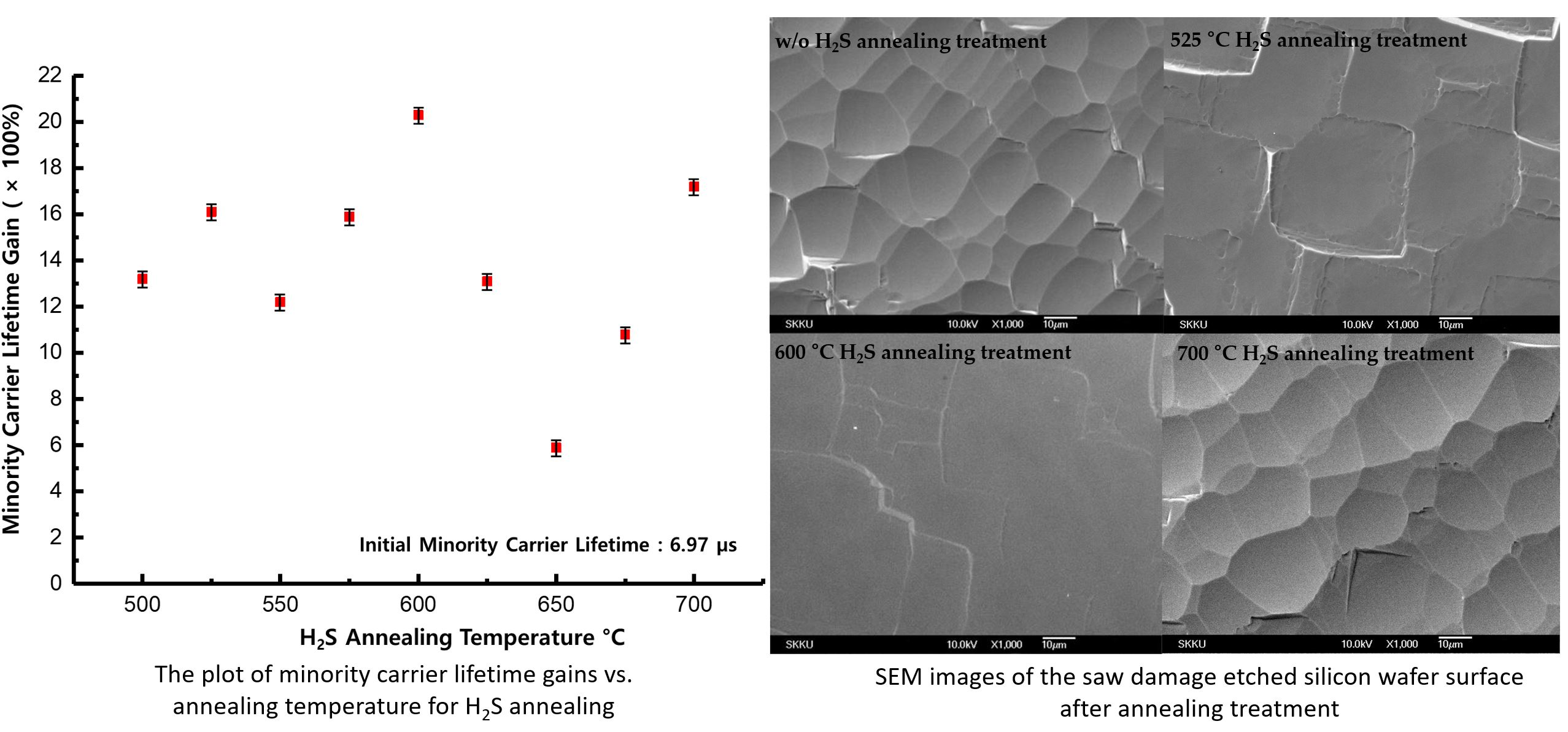
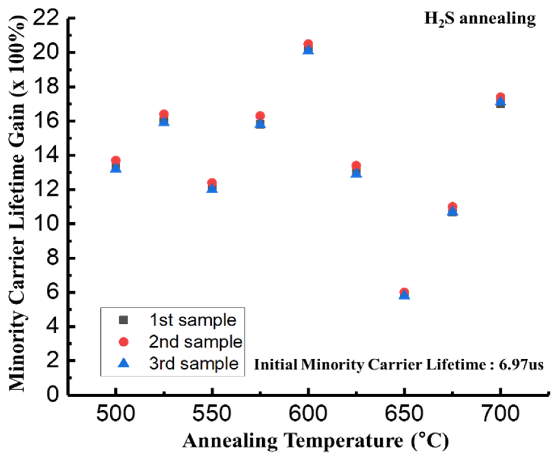
Figure 1. The plot of minority carrier lifetime gains vs. annealing temperature for H2S annealing.
Applsci 11 03527 g001
Figure 2. XPS spectra of S 2p for an H2S-passivated Si surface.
Applsci 11 03527 g002
Figure 3. XPS spectra of Si 2p for an H2S-passivated Si surface (700 °C).
Applsci 11 03527 g003
Figure 4. SEM images of the silicon surface: (a) saw damage etched wafer without H2S annealing treatment, (b) saw damaged etched wafer under 525 °C H2S annealing treatment, (c) saw damage etched wafer under 600 °C H2S annealing treatment, (d) saw damage etched wafer under 700 °C H2S annealing treatment.
Applsci 11 03527 g004
Figure 5. Electrostatic force microscopy (EFM) images of H2S (600 °C)-treated silicon wafers. (a,b) were measured under forwarding bias voltage, while (c,d) were measured under a reverse bias voltage.
Applsci 11 03527 g005
Table 1. Table of minority carrier lifetime gains vs. annealing temperature for H2S annealing (initial minority carrier lifetime: 6.97 µs).
H2S Annealing Temperature (°C)500525550575600625650675700
Minority carrier lifetime gain (×100%)
/standard deviation
13.2/
0.2517
16.1/
0.2646
12.2/
0.2
15.9/
0.3601
20.3/
0.1633
13.1/
0.2646
5.9/
0.1
10.8/
0.1732
17.2/
0.1732
Publisher’s Note: MDPI stays neutral with regard to jurisdictional claims in published maps and institutional affiliations.

