1. Introduction
Guided mode resonance (GMR) can occur when an incoming wave and output wave interfere in a waveguide [
1]. The spectral response depends on both the geometry and material of the waveguide and cladding layers. Both broad-band [
2] and narrow-band [
3] GMR filters with high transmittance/reflectance can be achieved by careful design. GMR has been used for filters [
4], absorbers [
5,
6,
7,
8], sensors [
9,
10], field enhancement [
11,
12], spectrometers [
13] and optical communications [
14].
Due to their ability to allow an intensive field enhancement, hybrid GMR systems that integrate plasmonic structures with photonic waveguide layers have also been developed. This property has been used for surface-enhanced Raman scattering (SERS) [
15], fluorescence enhancement [
16] and photodetectors [
17]. A gold nanoparticle array on top of an Indium Tin Oxide (ITO) waveguide layer has achieved strong coupling for bandgap engineering [
18]. A metal grating embedded in a high-index waveguide layer could produce an ultra-narrow transmission spectrum that has not been achieved using a single waveguide system or a single plasmonic system [
19]. High-index dye-doped polymer combined with metal nanostructures has also been explored [
20]. This scheme provides the ability to enhance the photoluminescence of the dye-doped polymer.
Although various configurations have been developed, almost all GMR structures use high-index materials as the waveguide layers since the Total Internal Reflection (TIR) must be satisfied at the top and bottom interfaces. This restricts GMR application in high-index material regions. Exploring GMR in a low-index waveguide can break the limitation and expand the GMR application into a broader condition. Therefore, it is an interesting question of whether low-index materials can also support a guided mode. While in the hybrid GMR system, the TIR can be replaced by the grating effect. This implies that one may realize the GMR in a low-index waveguide with the help of grating. Obtaining GMR in a low-index waveguide material expands the toolbox, especially for functional materials such as electro-optic polymers and mixed polymers with active materials.
In this paper, we clearly show that a guided mode resonance could be supported in a low-index waveguide material by adopting a hybrid GMR configuration and the refractive index of the substrate has little influence on the behavior of the guided mode resonance. In this scheme, the periodic metal gratings are embedded in the low-index waveguide layer which is situated on top of a high index substrate, and the air is used as the top cladding layer. The guided mode is supported by the combination of metal grating diffraction and the TIR. The TIR condition can be satisfied at the air-waveguide layer boundary. At the boundary between the low-index layer and the high-index layer, the diffraction of the metal grating couples the light wave into the waveguide and pushes the mode back into the low-index material. The guided mode resonance occurs when the diffracted light wave at the metal grating boundary and the TIR light wave at the top boundary match the waveguide mode supported by the low-index layer. The influence of the geometrical parameters on the GMR is explored with both simulation and experiment. This paper shows that almost all dielectrics no matter how large the refractive index is can be used to support GMR. The ease-of-fabrication makes this platform a promising candidate for many applications including sensing, imaging and fluorescence enhancement.
2. Design and Simulation
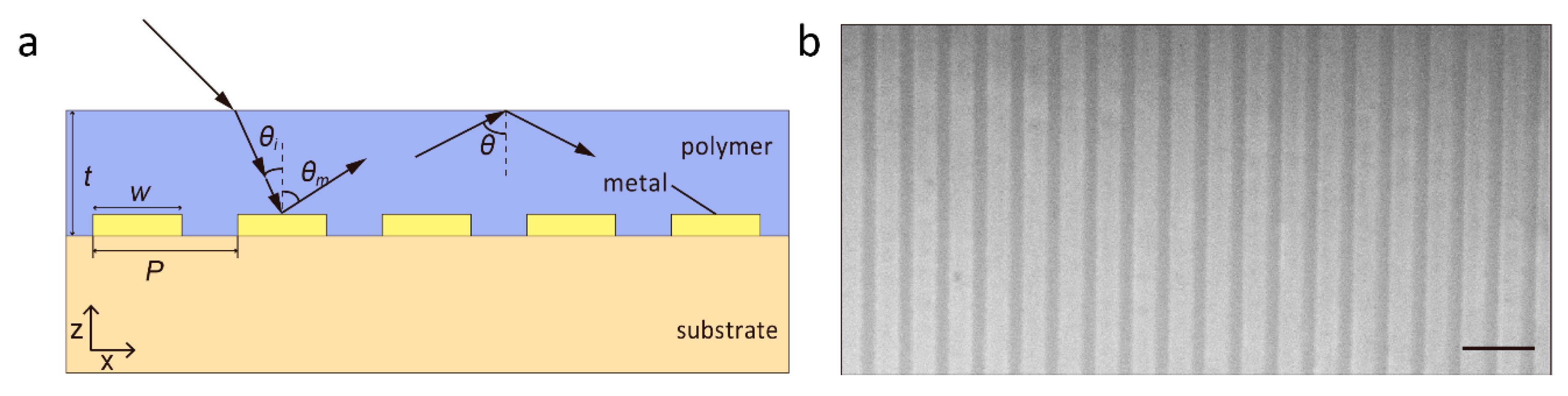
The proposed structure is shown in
Figure 1a. It consists of aluminum (Al) grating arrays embedded in a low-index waveguide layer. The waveguide layer sits on top of a high-index substrate. If there is no grating at the bottom boundary, then TIR cannot occur at the bottom interface as the refractive index of the waveguide layer is lower than the index of the substrate. On this condition, no guided mode can be supported. When a metal grating is inserted at the bottom interface, incident light could be diffracted from the interface. The TIR is effectively replaced by the grating diffraction at the bottom interface. The diffraction condition of the grating can be expressed as:
where
P is the grating period,
n is the refractive index of the waveguide layer,
represents the diffraction angle, subscript
m means the diffraction order and
is the wavelength in the vacuum.
is the angle of the incident light in the waveguide.
The metal grating used in this design acts as a ‘diffraction’ mirror. It plays two roles in the structure, coupling the incident light-wave into the guided mode and acting as a good mirror to push the light back into the waveguide. An extra phase is also provided by the metal grating like the TIR. For a perfect electrical conductor (PEC), the extra phase shift is π. For the slab waveguide bounded by the TIR effect and metal grating refraction effect, the guided mode resonance condition can be expressed as:
where
n is the refractive index of the waveguide layer,
t is the thickness of the waveguide layer,
is the wavenumber in a vacuum,
is the wavelength in vacuum,
θ is the incident angle of the guided mode wave in the waveguide, as shown in
Figure 1a,
and
denote the phase shift caused by the TIR and the metal grating. The TIR phase shift at the top boundary can be derived from Fresnel’s law as
and it depends on refractive index contrast, incident angle and the wavelength due to the dispersion of the refractive index, while the phase shift for metal
.
q is the mode order in the waveguide.
For the incident wave with a given wavelength, when the diffraction angle
matches to
θ, the guided mode can be excited in the waveguide. By combining Equations (1) and (2), the grating assisted guided mode resonance (GAGMR) condition can be expressed as:
Equation (3) shows that the guided mode resonance is related to the refractive index of the waveguide, the thickness of the waveguide and the grating period. The refractive index of the substrate has no direct influence on the guided mode but can affect the reflection intensity of the off-resonance wavelengths.
We evaluate the influence of the geometrical and material parameters on the guided mode using Finite Difference Time Domain (FDTD) simulation. The refractive indices of the substrate
and waveguide layer
n were fixed to be 2 and 1.5 to simplify the simulation. The material of grating was chosen as Al since it is relatively low loss and low cost. The refractive index of Al was adapted from reference [
21]. The thickness of the grating was 30 nm and the duty cycle was set to be 0.5. The top cladding layer was set to be air. A 2D simulation was used to decrease the simulation time. As shown in
Figure 1a, the broadband light wave (400 nm–800 nm) was propagated in the -Z direction and impinged on the waveguide layer. The perfectly matched layer (PML) boundary condition was set at the top and bottom
Z boundaries. Periodic boundary conditions were used for
X boundaries. Transverse electric (TE) polarized light with E-field parallel to the grating lines was used in this simulation, which eliminates the influence of the TM polarization of any plasmonic resonance. The polarization was not strictly limited to TE light if the GAGMR condition was satisfied. The reflection spectrum was collected by a power monitor behind the source.
We first examine how the grating period affects the guided mode. In this simulation, we used a normal incident plane wave as a light source (
). The thickness of the waveguide was fixed at 200 nm. The period was swept from 400 nm to 700 nm with a step size of 50 nm.
Figure 2a shows the calculated reflection spectra for various grating periods. For comparison, the reflection spectrum of the grating array (
P = 500 nm) without a waveguide layer is also shown. No apparent resonance but a small dip occurs in the bare metal gratings system. This small dip is due to the Wood-Rayleigh anomaly [
22], which happens both in bare metal gratings and gratings with a dielectric as cladding system (See
Figure 2a). This indicates that the waveguide layer can have a significant influence on the spectral features of the structures. As the period increases, the resonance shows a redshift, which is consistent with the grating diffraction Equation (1). The cutoff wavelength can be predicted by considering the boundary condition. At the air–waveguide boundary, the TIR condition:
must be satisfied. At the grating boundary, the diffraction angle for metal grating must be larger than the critical angle to couple the light wave back into the waveguide. Replacing
in Equation (1) with
and set
m = 1, we can get the cutoff wavelength as
. In
Figure 2a, we can see small drops at the cutoff wavelength for different periods. These drops caused by the Wood-Rayleigh anomaly can be a sign of the abrupt change of diffraction order. (See
Figure 2a.) As the diffraction angle of the metal grating cannot exceed 90 degrees, the maximum resonance wavelength is
.
Figure 2b shows the electric field amplitude profile in the
XZ plane, where the guided mode can be identified. The electric field intensity is enhanced 3.5-fold in the waveguide layer. In this configuration, the electric field is confined in the whole waveguide layer, which is different from the plasmonic system in which the electric hot spots are only near the metal gratings. This feature shows it could be used as an alternative structure for fluorescence enhancement.
Refractive index contrast can have a dramatic effect on the guided mode. In
Figure 3, we show how the guided mode resonance varies as a function of the refractive index of waveguide and substrate.
Figure 3a displays that the resonance peak redshifts as the refractive index of the waveguide increases. This can be explained by Fresnel’s equation although is not intuitive from Equation (3). The phase shift of
is a function of the refractive index of the cladding layer and the waveguide layer. Increasing the index contrast can increase the phase shift at the boundary and hence causes a redshift of the resonance wavelength. In
Figure 3b, as expected, no resonance shifts as the refractive index of the substrate changes. This implies that the metal grating diffraction effect can substitute for the TIR to couple and excite guided mode resonance in a waveguide layer. All the resonance peaks are not at unity due to the reflection loss of the metal. If we replace Al with a PEC in the simulation, the resonance peak can reach unity (shown in
Figure 3b).
Thickness is another substantial parameter for a guided mode. Equation (2) shows that increasing thickness will cause a redshift of the resonance and eventually a higher-order mode, just like higher-order guided mode arising in a thick or wide planar waveguide. There exists a cutoff ‘width’ below which no guided mode can be excited.
Figure 4a shows the relationship between thickness and the guided mode resonance. A cutoff thickness can be observed around 130 nm for the 1st order mode and around 350 nm for the 2nd order mode. The analytical results calculated by Equation (3) are consistent with the simulation and are also plotted in
Figure 4a (black triangles for the first order mode and red squares for the second order mode).
We also simulate the resonance character for different incident angles. As can be seen from
Figure 4b, for any non-zero incident angle, the resonance peak will split into two branches. One peak branch has a blueshift and another has a redshift as the incident angle increases. The sensitivity of resonant wavelength to incident angle is around 6.5 nm/degree. This consistent with Equation (3) which shows −1 and +1-order of guided mode resonance for a specific incident angle.
Besides, we have checked the tolerance of this structure. The simulation shows that decreasing or increasing duty cycle (DC from 0.4 to 0.6) has little influence on the performance of the resonance. The thickness of the gratings must be larger than 30 nm to avoid leaky light from the gratings. The performance is maintained for the thickness of the gratings above 30 nm. This large tolerance ensures ease of fabrication and application for this low-index waveguide system.
3. Experiment and Discussion
To characterize the guided mode resonance experimentally, the present structures were fabricated on a Lithium Niobate (LN) substrate (
). Electro-beam lithography was used to define the patterns on the substrate. Metal deposition and liftoff processes produced the metal gratings. After the grating fabrication, SU8 (
n = 1.6) was spin-coated on the gratings with different thicknesses to work as the waveguide layer. Reactive Ion Etching (RIE) was used to etch the SU8 layer to obtain various thicknesses.
Figure 1b shows the SEM picture of the fabricated structures before coating. The duty cycle of the fabricated grating is ~0.4 and the thickness of the metal grating array is 30 nm for all samples. We use the optical microscope (Olympus, BX53M) equipped with a spectrometer to characterize the performance of the guided mode resonance. As an example, we measure the transmittance spectra to confirm the existence of the resonance rather than reflectance due to the large field aperture of the microscope which requires a large sample size. The objective with NA = 0.1 was used for light collection. A linear polarizer was inserted between the light source and the sample to control the polarization of the incident light. All the spectra are calibrated with a blank LN substrate.
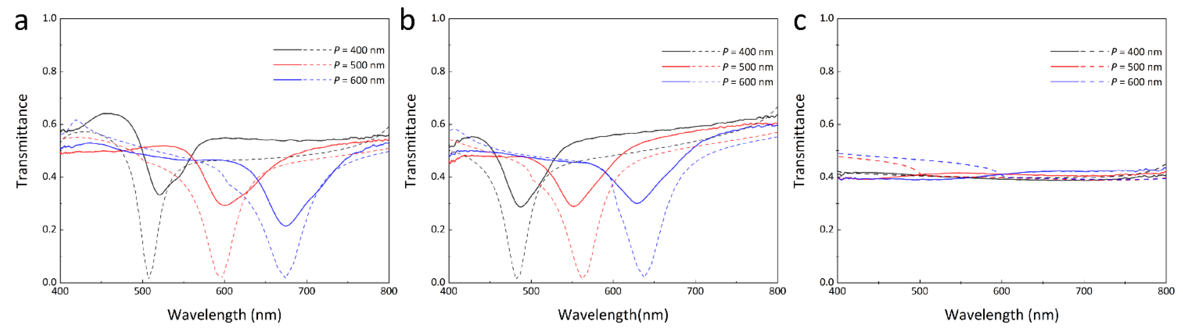
Figure 5 shows the experiment transmittance spectra for TE polarization. In
Figure 5a, the thickness of SU8
t = 205 nm. The periods of the gratings vary from 400 nm to 600 nm. Pronounced resonance dips can be observed in these spectra and these increase with the increase of the period. The simulated spectra for this device are also plotted in the figure with the dashed line. Good agreement can be seen from these spectra which indicates the presence of the guided mode resonances. The small divergence between simulation and measurement is due to two factors. Imperfections, such as roughness and inclusion on the metal gratings, can cause extra absorption which will introduce extra loss. Another factor is the small incident angle in the experiment. Both effects will broaden the resonance and decrease the quality factor (see
Figure 4b).
Figure 5b shows the transmittance of this device with a thickness of SU8
t = 172 nm. Compared with
Figure 5a, a blueshift of the resonance exists as expected. Like
Figure 5a, we simulate the transmittance spectra for this thickness. As can be seen from simulated results, the simulated spectra fit well with the experiment results. We also measured and simulated the spectra of the gratings with no SU8 waveguide layer. As shown in
Figure 5c, no obvious resonance occurs. This implies that the resonance is surely caused by the guided mode resonance in the SU8 waveguide layer.
As shown by simulation and experiment, we demonstrate that the GMR can exist in the low-index waveguide layer made of SU8 polymer. Pronounced resonance dips occur in the transmittance spectra due to the GMR effect and all these dips follow the behavior as predicted. These results reveal that, with the help of metal gratings, any dielectric could be used as the core waveguide for GMR regardless of the refractive index of the substrate. By tuning geometrical parameters, we could control the GMR wavelength in a specific spectrum region. This feature applies large freedom for device design. Due to the resonance wavelength being sensitive to parameters such as thickness, angle, and refractive index, the proposed device may be a good candidate for sensing application. This novel structure provides exciting features compared with previous work. One can excite GMR in any material regardless of the refractive index. This releases the limitation of traditional GMR devices which need a high-index waveguide to support the resonance. This is a big advancement since previous works [
20] can only use a high-index polymer to achieve fluorescence enhancement. This property makes it possible that we could use more functional materials for fluorescence enhancement. Besides, there could be an opportunity in the infrared regime where high-index material such as silicon and germanium are the typical substrate for most applications.


