1. Introduction
Microdevices comprising of film layers have been used in a wide range of fields, such as semiconductors, solar photovoltaic industries, and material sciences [
1,
2,
3]. The film structure metrology is an essential area, since the qualitative and quantitative analysis of film structures provides insight into the influence of manufacturing processes on functional characteristics [
4,
5].
In past decades, optical techniques have drawn much attention in the characterization of thin material layers due to their ability to provide nondestructive measures. The most well-established of these are ellipsometers, reflectometers, and white-light interferometry (WLI) [
6,
7,
8]. Ellipsometers and reflectometers are used in many cases, since they can measure the layer thickness and refractive index of thin films [
9,
10]. However, to provide a full-field thickness profile as well as the topography of the corresponding surfaces, these two approaches both require a time-consuming process or complicated system configuration. Another method, WLI, fulfills the requirements of high efficiency for the 3D inspection of the internal structure of a film. Although WLI allows the simultaneous measurement of a film surface and substrate surface with a high precision [
11,
12,
13], the interference originating at each surface imposes strict demands on the reconstruction algorithm and library of theoretical signals.
Recently, Xie et al. introduced structured illumination microscopy (SIM) into the field of film measurement because the SIM-based method has a high axial resolution and efficiency in 3D measuring [
14,
15,
16,
17,
18,
19]. In SIM, several sinusoidal patterns with predefined phases are projected on the sample surface. The modulation distribution of the captured images reflected from the surface can be determined by the phase-shifting technique [
20]. The modulation depth response (MDR) curve of each pixel, which indicates the modulation distribution on the point changing with the scanning distance, can be achieved by vertically scanning the sample around the focal plane. Therefore, detecting the peak of the MDR curves makes it easy to reconstruct the three-dimensional surface topography. When SIM is applied in the film structure measurement, the MDR involves several peaks as the projected sinusoidal pattern reflects on the corresponding surfaces. As a result, the surface profiles and film thickness can be obtained by identifying the peaks.
However, when the thickness between adjoining layers is thinner, the peaks of the MDR start to overlap to create distorted peaks. As the extent of the peak overlap increases, the change in the peak shape is enlarged, amplifying the location extraction error and decreasing the accuracy in conventional SIM. Further, if the overlapped peaks are bent into one, the traditional methods become failed because they find the only maximum point. Consequently, the maximum-point-based approach has a circumscribed thickness resolution, which limits the application for SIM in the field of film structure measurement.
To develop the measurement threshold of thickness in SIM, we developed a new method iterative peak separation structured illumination microscopy (IPS-SIM). Since the incoherent light reflected from the sample is the combination of reflections from the surface of the interior layers, the MDR curve can be considered as a Gaussian model. For a single-film-layer sample, the MDR curve is a sum of two Gaussian functions. To optimize the location of each peak of the MDR, the IPS-SIM utilizes the iterative optimization algorithm of which the model function is the sum of Gauss. Compared with the traditional SIM, the proposed method provides accurate peak detection even when the peaks of the MDR are highly overlapping. Then, the precise location of peaks is used to determine the height of the layers. Hence, the IPS-SIM provides a lower detection threshold for thickness than the existing SIM method for film thickness profile measurement. In this work, a theoretical analysis and simulation are conducted to validate the use of IPS-SIM in analyzing film structures. Experiments on a single photoresists layer deposited on silicon slides demonstrate the feasibility of this method and confirm that the repeatability is within 2 nm.
2. Methods
2.1. Principle of Surface and Thickness Method
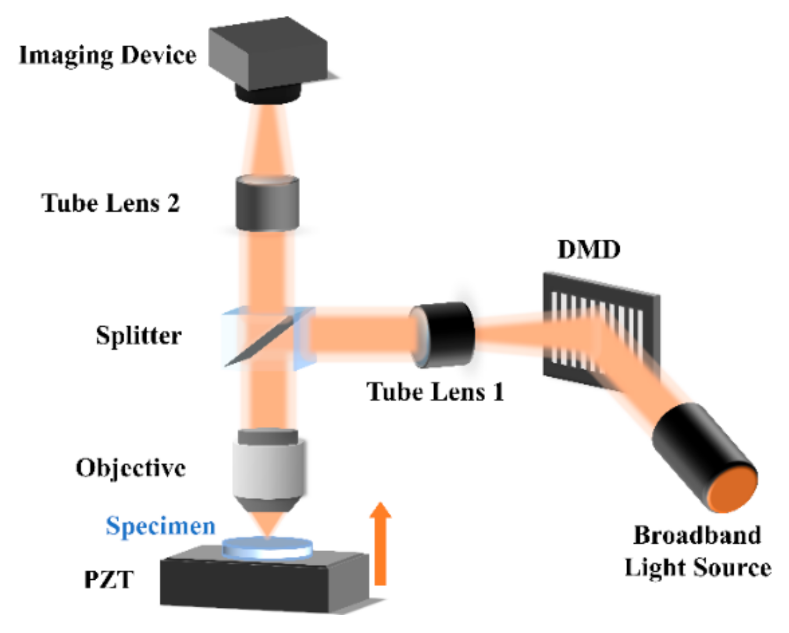
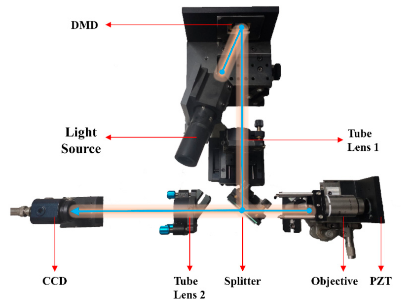
The schematic diagram of the measurement system is illustrated in
Figure 1. The incident light from a light-emitting diode (LED) light source was modulated by a digital micro-mirror device (DMD), then collimated by the tube lens before being reflected by the splitter mirror into the objective microscope lens. The fringe patterns on the DMD chip were projected onto the sample located in the focal plane. The charge-coupled device (CCD) camera behind the other tube lens captured the signal containing reflections taking place in the top surface of the film and the substrate. While the specimen is scanned in a
z-axis direction by the piezoelectric transducer (PZT) stage, the fringe contrast response of modulated images can be used to characterize the thickness profile of the specimen.
If we suppose that projected patterns are sinusoidal gratings, the light intensity distribution on the captured images can be written as:
where
illustrates the background irradiance and
describes the modulation distribution of the projected sinusoidal fringe pattern, of which the spatial frequency is
and the initial phase is
. The modulation distribution of each pixel can be determined by a phase-shifting algorithm [
21,
22]. In order to minimize the uncertainty caused by the process of modulation evaluation, the fringe for each scanning step was laterally shifted eight times in this study.
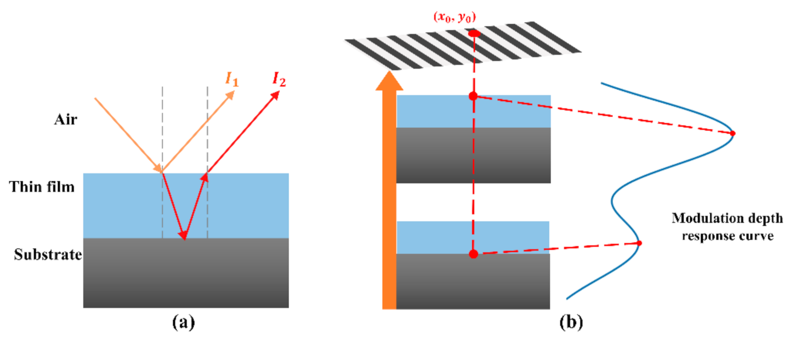
When measuring a sample with a single film layer as shown in
Figure 2a, the projected fringe pattern was reflected from the film surface and the substrate. Suppose that
presents the film layer and the substrate and
. Consequently, the light intensity distribution is given as:
Hence, the fringe modulation distribution
in Equation (1) is composed of two corresponding component signals and can be written as:
As determined in the study of Stokseth [
23], the normalized modulation depth response (MDR) of the individual surface is approximately a Gaussian function with an independent variable scanning position
, which can be described as:
Here,
indicates the reflectivity of the thin film;
describes the focal position;
presents the scanning distance—i.e., the defocus distance from the focal position; and
.
is an acronym for the full width at half maximum and can be determined by [
23]:
where
denotes the wavelength of the light source;
indicates the refraction index;
is the normalized spatial frequency of the sinusoidal fringe pattern—i.e.,
;
describes the period of the sinusoidal fringe pattern; and
NA presents the numerical aperture of the objective lens.
For the arbitrary pixel
on the sample in
Figure 2b, by substituting Equation (4) into Equation (3) the MDR curve is theoretically expressed as:
Here, and are the coefficient of the modulation component on the film and the substrate, which is influenced by the absorption, transmission, and reflection of the film layer; the reflectivity of the substrate; and the film thickness.
As shown in
Figure 2b, the MDR reaches its maximal value when the related point on the layer is in the imaging plane. Therefore, the film thickness and the surface profiles can be determined by the identification of the location of peaks
and
. The physical thickness of thin film
at the point is calculated by:
where
describes the refraction index of the thin film.
2.2. Iterative Peak-Separation Method
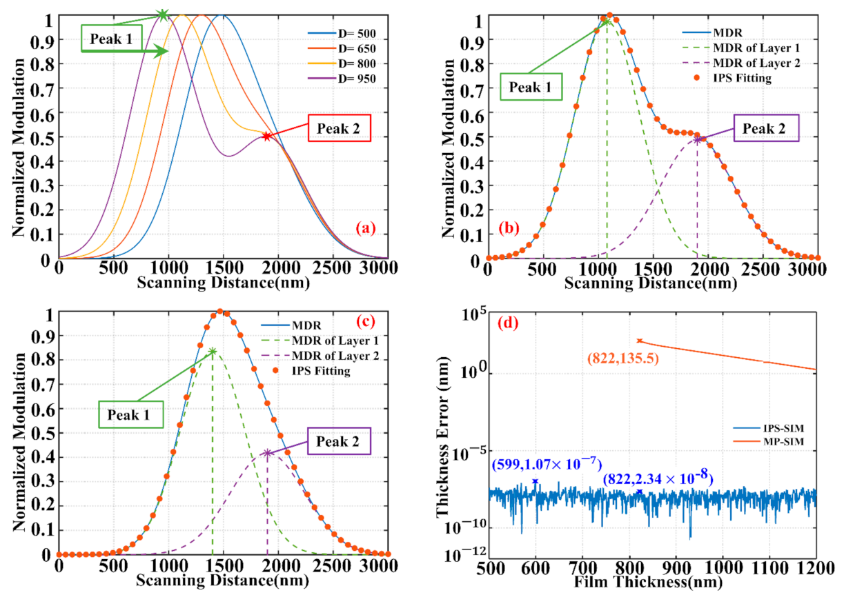
As previously mentioned, a valid measurement depends on the accurate extraction of the peak locations. The base of the peak location is to find the maximum in the existing method, so it is called the maximum-point-based SIM (MP-SIM). When the MDR has only one peak shape due to the film being thinner, as shown by the blue curve in
Figure 3a, the MP-SIM only detects one peak and fails to calculate the film thickness. Therefore, the detection threshold is limited. We propose the iterative curve fitting technique to break the limit.
To shorten the time required to fit the full-field MDR curve, the Nelder-Mead simplex algorithm is utilized. According to Equation (6), the model function
is defined as:
where the linear variables are the component coefficients—i.e.,
and
—and the nonlinear variables are the full width at half maximum (i.e.,
and
) and the peak positions (i.e.,
and
). Finding the location of overlapping peaks—i.e.,
—can be transformed into an optimization problem, such as:
Suppose that the thickness measurement error is the criterion for the threshold. The comparison proves that the smallest detectable thickness of the IPS-SIM is lower than the MP-SIM, as illustrated in
Figure 3. When the film thickness is 822 nm, the measurement error of the MP-SIM equals 135.5 nm. On the contrary, the IPS-SIM accurately identifies the two peaks, as shown in
Figure 3b. Furthermore, the presented algorithm still maintains a low measurement error when the two components are completely merged into one, as explained in
Figure 3c. The thickness measurement error as a function of film thickness in the two methods is illustrated in
Figure 3d. The results show that the IPS-SIM has a lower detection threshold than the MP-SIM.
3. Simulations
In practice, the MDR curve is not a perfect Gaussian shape due to the induced noise in the single-pixel spectra and the higher harmonic effect. The smoothing cannot average the measurement uncertainty in peak positioning. For a reasonable solution and a fast convergence rate, the IPS-SIM requires a good starting value. Mathematical analysis and numerical simulation were conducted to analyze the best initial of iterative variables in this section.
Suppose that the thickness , the component coefficient and , the numerical aperture of the objective , the central wavelength of the light source , and the normalized spatial frequency of the fringe pattern . Thus, the hypothetical is calculated as 696 nm. Owing to the influence of the film layer, is larger than and is set to be 800 nm. The random noise of 2% modulation is added in the simulation to match reality more precisely.
3.1. Optimization of Initial Full Width at Half Maximum
The initial value of and , , had a significant effect on the measurement accuracy. Although the theoretical can be calculated according to Equation 5, the was an experimental parameter related to the characteristics of film and the environmental factors. There are even cases where not all the parameters in Equation (5) are known, failing to determine the ideal . According to the intrinsic constraints, i.e., the full width at half maximum is non-negative, there are several methods to obtain the start of the full width at half maximum:
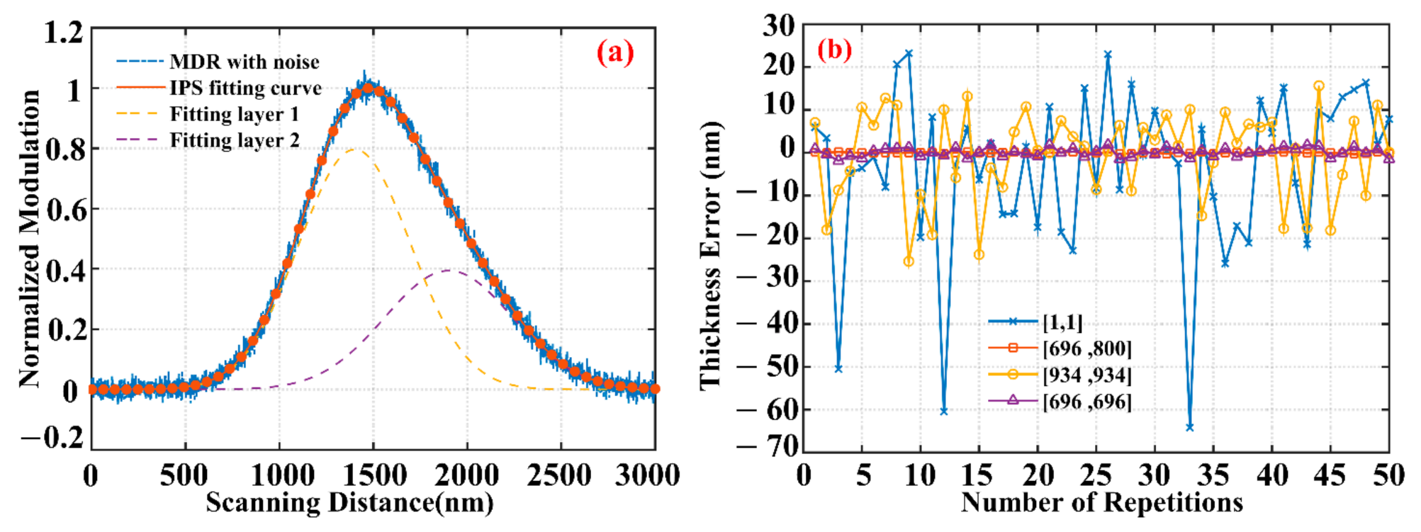
The smallest non-negative integer—i.e., (1, 1);
The experimental of the overlapping-peak MDR—i.e., (934, 934);
The theoretical —i.e., (696, 696);
The default—i.e., (696, 800);
To compare the performance in these four cases, we independently measured the thickness at a fixed position by the IPS-SIM 50 times.
Figure 4a illustrates one of the simulated MDR and the fitting result, as the initial widths
(696, 696). The error of thickness detection, as shown in
Figure 4b, indicates that the theoretical
is the optimal start point because it has a detection error (purple and marked with triangles) closest to the true-value way (orange and marked with squares) and can be implemented in the application.
3.2. Influence of Initial Component Coefficient
Although the component coefficient,
, varies with multiple parameters such as reflectivity and film thickness, physical constraints including non-negativity and the range (from zero to one) are required. To reduce variables, the initial value of width was fixed as
, and
starts from 0.8. The measurement results with a different initial
are shown in
Figure 5.
The center point of the error bar represents the mean error of 50 measurements. The maximum absolute error is less than 3 nm, which indicates that the IPS-SIM is high-accuracy. The longitudinal length of the bar is the standard deviation and becomes longer as the difference between the initial value and default is larger. As a result, the standard deviation is positively related to the deviation between the iteration start point and the set value.
3.3. Influence of Initial Peak Position
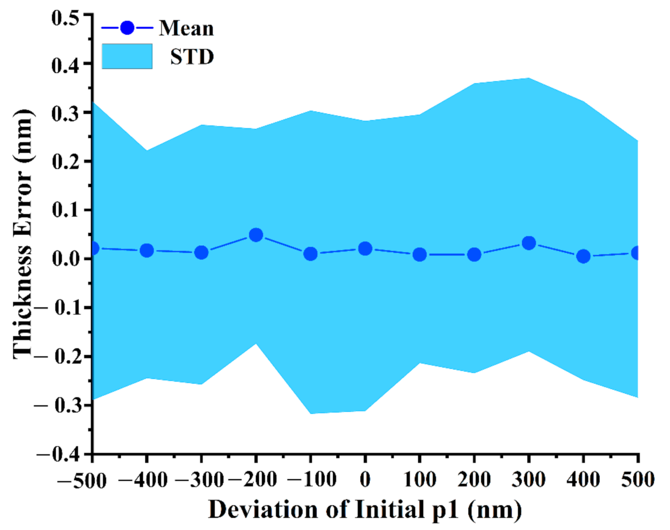
In the above analysis, the initial value of the peak position is defined as [1, 1]. Therefore, if the initial value of widths and component coefficients is proper, the accuracy of the IPS algorithm is high. Assuming that the initial value of the width is , the start point of the component coefficients is , and the iterates from 1900 nm, we analyze the influence of the initial point of on the measurement accuracy.
Figure 6 illustrates the measurement results, of which the horizontal axis center is the deviation between the start value of
and the simulated value of 1400 nm. The connect center point of the error bar describes the mean error of 50 measurement times. The shaded area of the bar is the standard deviation. The mean error is within 0.05 nm, and the standard deviation is between −0.31 to 0.35, which indicates that the start point of peak positions has little effect on the accuracy of the IPS-SIM.
4. Experiment
In order to validate the performance of the mentioned method, experiments were conducted on the sample with the photoresist film layer. The system was performed by referring to
Figure 1, with a scanning stage (PI, the resolution is ± 0.5 nm), a microscopy objective (Olympus, 100X, NA = 0.9), a CCD camera (WAT-902H, 576 × 768 pixels, pixel size 6.25 × 6.25 um), a 1024 × 768 pixels DMD (TI) with the pixel resolution 13.6 um, an LED broadband light source (central wavelength is 580 nm, bandwidth is 160 nm), and two tube lenses provided by DAHENG Optics. The diagrams of the layer structures on the samples are shown in
Figure 7.
In the experiment, the film was made by a photoresist RZJ-304 on the wafer using a spin coater. The refractive index provided by Filmetrics was 1.674. The pattern was formed on the silicon substrate through the photolithography process. The PZT stage scanned 4 um with the stepping pace of 50 nm in the z-direction. For each step, the pattern with the period of 16 pixels was shifted by phase to calculate the modulation distribution, and the experimental value of was calculated as 1443 nm. Then, the peak location of the MDR for each pixel was extracted using the IPS method.
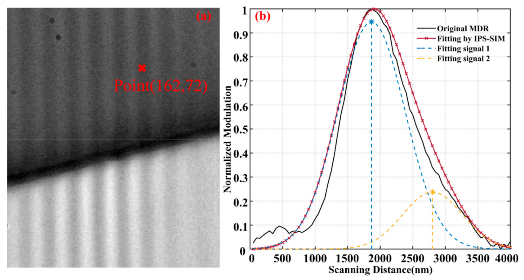
Figure 8a shows the captured image at the scanning distance of 1700 nm. The black line in
Figure 8b is the original MDR curve of a pixel at the photoresist area. Although the fitting curve (red and plus-marked) obtained by the IPS-SIM does not entirely match the simulation, the peaks (blue and yellow star) are successfully separated. The thickness at the point obtained by the presented method is 1382.47 nm.
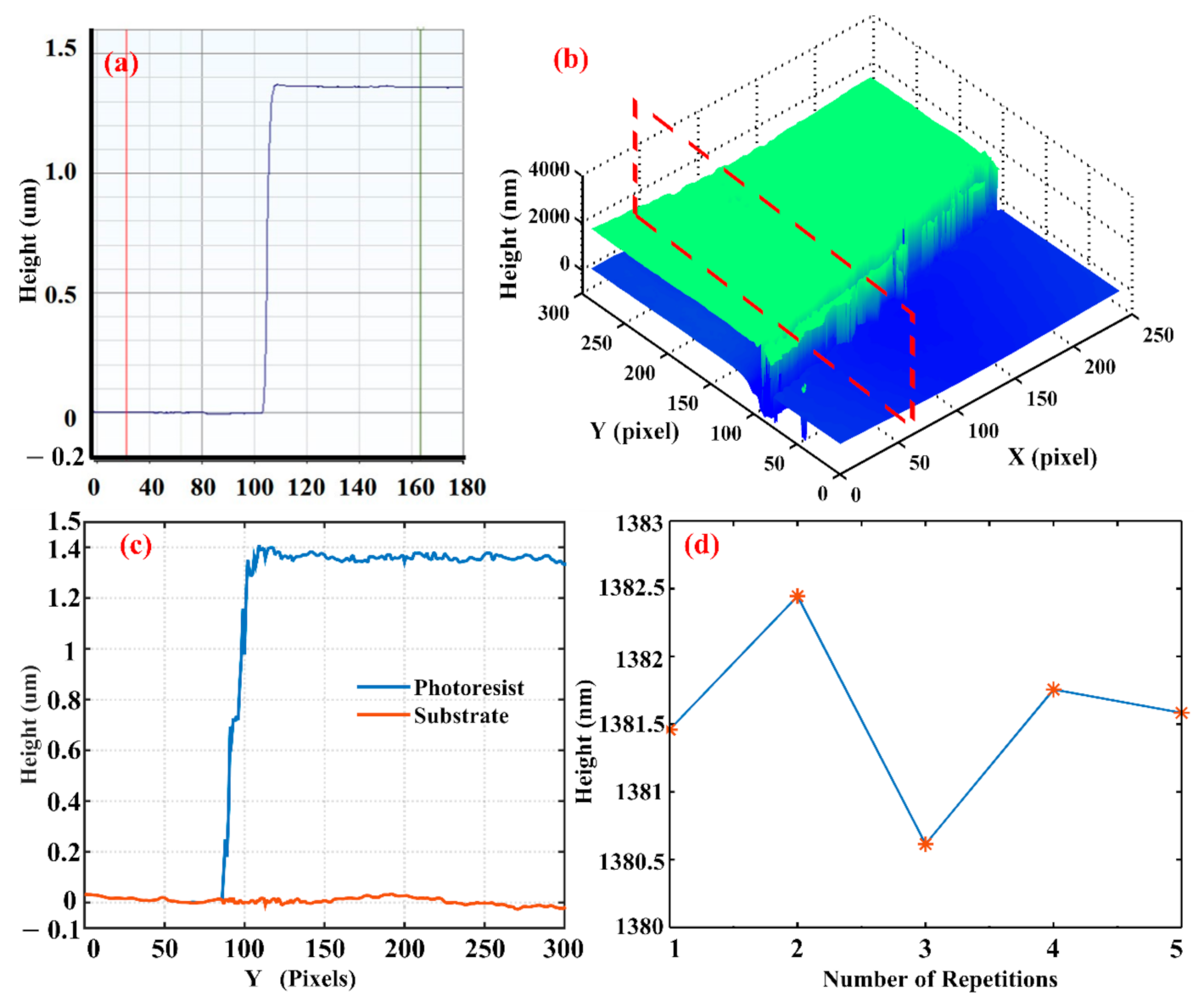
To confirm the accuracy of the developed method, we made a comparison between the commercial Profilometer and the IPS-SIM. The measurement provided by the commercial Profilometer is 1364.60 nm, as presented in
Figure 9a. This result demonstrates that the relative uncertainty of the IPS-SIM is less than 17.80 nm. The 3D structure of the sample is reconstructed, as shown in
Figure 9b. The cross-section profile at X = 70 is presented in
Figure 9c. Furthermore, five repetitive tests were carried out to estimate the repeatability of the proposed method.
Figure 9d describes the measured result at the same point five times, which indicates that the repeatability of the measurements is less than 2 nm.
5. Conclusions
There are several comments that can be made regarding the above results:
The significant standard deviation for thickness is due to the large side lobes of the MDR curve. At some pixels, these high-level side lobes are fitted as the second-highest peak, so the error of thickness is larger. The original influence induced in the measurement process can affect the level of the side lobe. Thus, in the absence of the cause of the side lobe, there is no a priori knowledge to reduce this error.
The R-square in the experiment was smaller than the theoretical value. There is a considerable error between the experimental value of and the theoretical value of , which is set to the start point of in this study. For the same film material, starting from the empirical value obtained by pre-calibration can produce a higher fitting degree.
Although the IPS algorithm has a faster computation speed than other iterative algorithms, the proposed approach is more time-consuming than the MP-SIM. Further study on improving the efficiency of the fitting process would enhance the method’s performance.
In conclusion, we proposed and experimentally validated a method, named iterative peak separation structured illumination microscopy (IPS-SIM), to develop the detection threshold of thickness in SIM. When the MDR curve peaks are too overlapping and bent into one, the traditional maximum-point-based technique (MP-SIM) has no ability to recognize each peak and measure the thickness and surface profile. In order to overcome the limitation, this study suggests obtaining the peak location of the modulation depth response (MDR) curve by the optimization algorithm. The mentioned method can provide a lower measurement threshold and high precision if the iterative variable has a good start value. In this paper, the influence of each parameter on the measurement accuracy is numerically analyzed and the optimal initial value of each parameter is determined. Single-film-layer specimens coated with photoresist are measured to verify the feasibility of the IPS-SIM and its lower detection threshold than the conventional approach.
Author Contributions
Conceptualization, K.Y. and Y.T.; methodology, K.Y. and Z.X.; software, J.F. and C.H.; validation, K.Y., Z.X. and C.H.; formal analysis, K.Y. and Y.T.; investigation, K.Y.; writing—original draft preparation, K.Y.; writing—review and editing, K.Y. and Y.T.; supervision, Y.T. and S.H.; funding acquisition, S.H. and Y.T. All authors have read and agreed to the published version of the manuscript.
Funding
This research was funded by the National Natural Science Foundation of China, grant number 61875201, 61975211, and 62005287; the Sichuan Science and Technology Program, grant number 2019JDRC0064, 2020JDJQ0005, and 2020ZYD020.
Institutional Review Board Statement
Not applicable.
Informed Consent Statement
Not applicable.
Data Availability Statement
Data is contained within the article.
Acknowledgments
The authors gratefully thank Y.Q. for his assistance during the experiment.
Conflicts of Interest
The authors declare no conflict of interest.
References
- Park, K.K.; Lee, H.; Kupnik, M.; Khuri-Yakub, B.T. Fabrication of capacitive micromachined ultrasonic transducers via local oxidation and direct wafer bonding. J. Microelectromech. Syst. 2011, 20, 95–103. [Google Scholar] [CrossRef]
- Huang, F.; Pascoe, A.R.; Wu, W.-Q.; Ku, Z.; Peng, Y.; Zhong, J.; Caruso, R.A.; Cheng, Y.-B. Effect of the microstructure of the functional layers on the efficiency of perovskite solar cells. Adv. Mater. 2017, 29, 1601715. [Google Scholar] [CrossRef]
- Lyu, J.; Liu, Z.; Wu, X.; Li, G.; Fang, D.; Zhang, X. Nanofibrous kevlar aerogel films and their phase-change composites for highly efficient infrared stealth. ACS Nano 2019, 13, 2236–2245. [Google Scholar] [CrossRef]
- Kim, Y.; Hibino, K.; Hanayama, R.; Sugita, N.; Mitsuishi, M. Multiple-surface interferometry of highly reflective wafer by wavelength tuning. Opt. Express 2014, 22, 21145–21156. [Google Scholar] [CrossRef] [PubMed]
- Bakhtazad, A.; Chowdhury, S. An evaluation of optical profilometry techniques for CMUT characterization. Microsyst. Technol. 2019, 25, 3627–3642. [Google Scholar] [CrossRef]
- Mccrackin, F.; Passaglia, E.; Stromberg, R.; Steinberg, H. Measurememt of thickness and refractive index of very thin films and optical properties of surfaces by ellipsometry. J. Res. Natl. Bur. Stand. Sect. Phys. Chem. 1963, 67, 363. [Google Scholar] [CrossRef]
- Youngquist, R.; Carr, S.; Davies, D. Optical coherence-domain reflectometry: A new optical evaluation technique. Opt. Lett. 1987, 12, 158–160. [Google Scholar] [CrossRef]
- Kim, S.-W.; Kim, G.-H. Thickness-profile measurement of transparent thin-film layers by white-light scanning interferometry. Appl. Opt. 1999, 38, 5968–5973. [Google Scholar] [CrossRef] [PubMed]
- Papa, Z.; Csontos, J.; Smausz, T.; Toth, Z.; Budai, J. Spectroscopic ellipsometric investigation of graphene and thin carbon films from the point of view of depolarization effects. Appl. Surf. Sci. 2017, 421, 714–721. [Google Scholar] [CrossRef]
- Yun, Y.; Joo, K.-N. Novel combined measurement system to characterize film structures by spectral interferometry and ellipsometry. Opt. Express 2018, 26, 34396. [Google Scholar] [CrossRef]
- Hlubina, P.; Ciprian, D.; Luňáček, J. Spectral interferometric technique to measure the relative phase change on reflection from a thin-film structure. Appl. Phys. B 2010, 101, 869–873. [Google Scholar] [CrossRef][Green Version]
- De Groot, P. Principles of interference microscopy for the measurement of surface topography. Adv. Opt. Photon. 2015, 7, 1–65. [Google Scholar] [CrossRef]
- Zhou, Y.; Tang, Y.; Zhu, J.; Deng, Q.; Yang, Y.; Zhao, L.; Hu, S. Characterization of micro structure through hybrid interference and phase determination in broadband light interferometry. Appl. Opt. 2017, 56, 2301–2306. [Google Scholar] [CrossRef]
- Gustafsson, M.G.L.; Shao, L.; Carlton, P.M.; Wang, C.J.R.; Golubovskaya, I.N.; Cande, W.Z.; Agard, D.A.; Sedat, J.W. Three-dimensional resolution doubling in wide-field fluorescence microscopy by structured illumination. Biophys. J. 2008, 94, 4957–4970. [Google Scholar] [CrossRef]
- York, A.G.; Chandris, P.; Nogare, D.D.; Head, J.; Wawrzusin, P.; Fischer, R.S.; Chitnis, A.; Shroff, H. Instant super-resolution imaging in live cells and embryos via analog Image processing. Nat. Methods 2013, 10, 1122–1126. [Google Scholar] [CrossRef]
- Wang, C.-C.; Lee, K.-L.; Lee, C.-H. Wide-field optical nanoprofilometry using structured illumination. Opt. Lett. 2009, 34, 3538. [Google Scholar] [CrossRef] [PubMed]
- Zhang, Q.; Su, X.; Cao, Y.; Li, Y.; Xiang, L.; Chen, W. Optical 3-D shape and deformation measurement of rotating blades using stroboscopic structured illumination. Opt. Eng. 2005, 44, 113601. [Google Scholar] [CrossRef]
- Xie, Z.; Tang, Y.; Zhou, Y.; Deng, Q. Surface and thickness measurement of transparent thin-film layers utilizing modulation-based structured-illumination microscopy. Opt. Express 2018, 26, 2944. [Google Scholar] [CrossRef] [PubMed]
- Xie, Z.; Tang, Y.; Wei, H.; Liu, J.; He, Y.; Hu, S. Optical sectioning microscopy for multilayer structure with micro-scale air gaps measurement. IEEE Photon. Technol. Lett. 2019, 31, 141–144. [Google Scholar] [CrossRef]
- Neil, M.A.A.; Juskaitis, R.; Wilson, T. Method of obtaining optical sectioning by using structured light in a conventional microscope. Opt. Lett. 1997, 22, 1905–1907. [Google Scholar] [CrossRef]
- Kim, Y.; Hibino, K.; Sugita, N.; Mitsuishi, M. Design of phase shifting algorithms: Fringe contrast maximum. Opt. Express 2014, 22, 18203–18213. [Google Scholar] [CrossRef]
- Dan, D.; Yao, B.; Lei, M. Structured illumination microscopy for super-resolution and optical sectioning. Chin. Sci. Bull. 2014, 59, 1291–1307. [Google Scholar] [CrossRef]
- Stokseth, P.A. Properties of a defocused optical system. J. Opt. Soc. Am. 1969, 59, 1314. [Google Scholar] [CrossRef]
| Publisher’s Note: MDPI stays neutral with regard to jurisdictional claims in published maps and institutional affiliations. |
© 2021 by the authors. Licensee MDPI, Basel, Switzerland. This article is an open access article distributed under the terms and conditions of the Creative Commons Attribution (CC BY) license (https://creativecommons.org/licenses/by/4.0/).
