Abstract
Interleaved power factor correction (PFC) is widely used circuit topology due to good efficiency and power density for single-switch boost PFC. As the differential mode (DM) electromagnetic interference (EMI) noise magnitude depends upon the input current ripple, this research details a comprehensive study of DM EMI filter design for interleaved boost PFC with the aim of minimizing the component size. It is also demonstrated that the different numbers of interleaved stages and switching frequency influence the filter attenuation requirement and, thus, the EMI filter size. First, an analytical model is derived on the basis of the Norton equivalent circuit model for the differential mode noises of interleaved boost PFC within the frequency range of 9–500 kHz. The derived model can help identify the proper phase shifting among the interleaved boost converters in order to minimize the considered differential mode noises at the filter design frequency. So, a novel phase-shift method is developed to get a minimized attenuation required by a filter in Band B. Further, a volume optimization of the required DM filter was introduced based on the calculated filter attenuation and volumetric component parameters. Based on the obtained results, unconventional and conventional phase shifts have demonstrated a good performance in decreasing the EMI filter volume in Band B and Band A, respectively. A 2-kW interleaved PFC case study is presented to verify the theoretical analyses and the impact of phase-shifting on EMI filter size.
1. Introduction
Complying with harmonic standards and power factor requirement of the input AC power has resulted in the development of boost power factor correction (PFC) circuits to get an improved power factor close to unity. Additionally, using interleaving PFC, numerous benefits are obtained, including an increased power density, reduced overall design volume, and declined RMS current flowing through the boost capacitor, and using an interleaved configuration leads to a significant decrease in the switching frequency ripples as a result of the ripple cancelation effect [1]. Notably, this application is employed to ensure sinusoidally shaped input currents in connection with differential mode (DM) electromagnetic interference (EMI) input filters, limiting the high-frequency noise transmission from the converter to the power grid [2]. However, the increased integration of power electronics converter into the grid results in some challenging EMI issues because of inherent pulse energy conversion characteristics. Thus, the unwanted emissions should be suppressed to fulfill noise emission standards, such as CISPR-11 for frequencies beyond 150 kHz [3]. Because of the increasing demand for pulse-width modulation (PWM) converters, a number of standards are defined below the frequency of 150 kHz in some applications, CISPR-14 (induction hubs) [4], and CISPR-15 (lighting equipment) [5]. Moreover, the CISPR 16-1-1 is split into two main frequencies as Band-A (9–150 kHz) and Band-B (150 kHz–30 MHz) [6]. An EMI estimation approach and EMI filter designing analysis are proposed for the 9–500 kHz based on the following assumptions:
- DM noise estimation is only considered. A type of noise current is flowing in the same direction as the power supply current, known as “DM,” because the outgoing and return currents are reversely directed.
- Rise time and fall time of switching waveform effects are ignored in the model.
- DM EMI filter is analyzed from the volume optimization point of view. Analysis is not covering the common mode EMI filter volume optimization.
- Parasitic component effects are negligible.
EMI filter is effectively employed for reducing the EMI noise emissions, which is designed based on the required noise attenuation requirements. The EMI filter’s dependency on the EMI noise’s peak value has led to many modeling approaches to estimate the EMI noise peak in the Bands A and B frequency ranges [6,7,8,9,10]. Additionally, it is highly acceptable that the reduced grid input ripple current results in the reduction of the DM EMI noise magnitude and filter attenuation requirements, which make the DM EMI filter size smaller and the corner frequency higher [1]. So far, the EMI filter has been designed based on Band-B considering the presence of noise criteria within the frequency standards above 150 kHz [11]. Recently, Band-A has become important due to the advent of new standards. Notably, Band-A’s design DM EMI filter provides enough damping in Band-B to shift the filter corner frequency within the low frequencies. In the past decade, higher efforts have been carried out to estimate the DM EMI noise emission. Additionally, most of the modeling approaches that have been focusing on EMI analysis within a frequency range above 150 kHz are based on simulations [7,8]. Notably, prior state-of-the-art simulation-based methods may be quite cumbersome if scaled up for system-level studies.
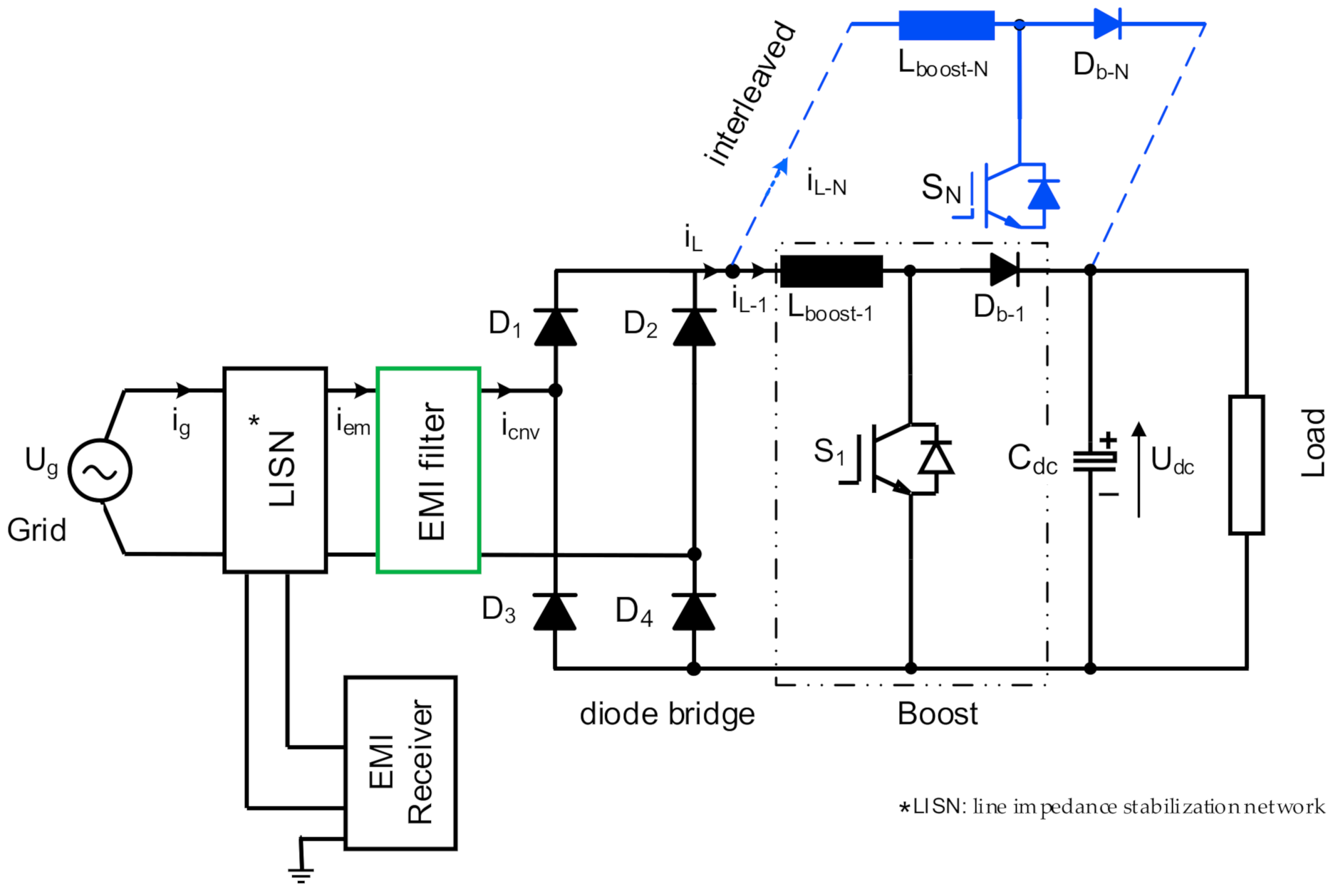
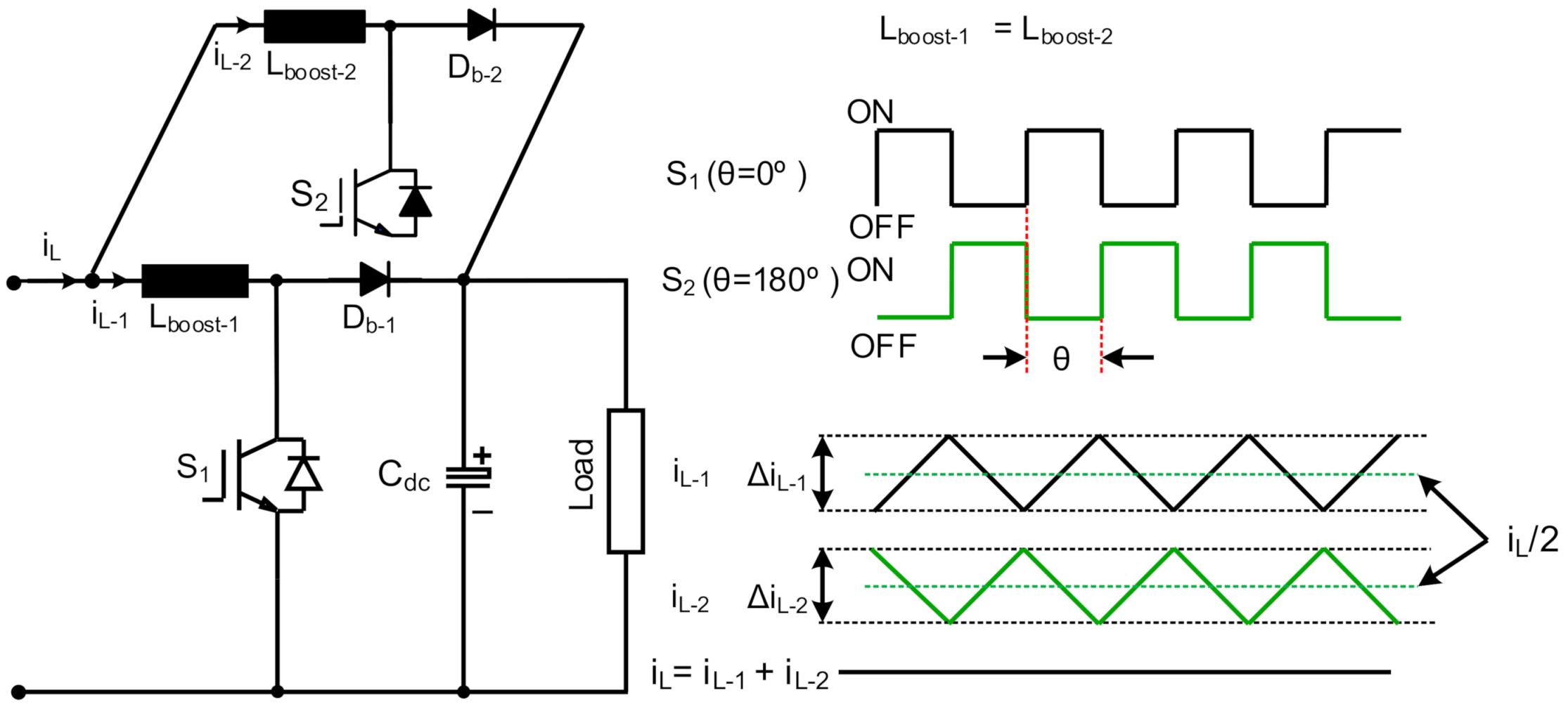
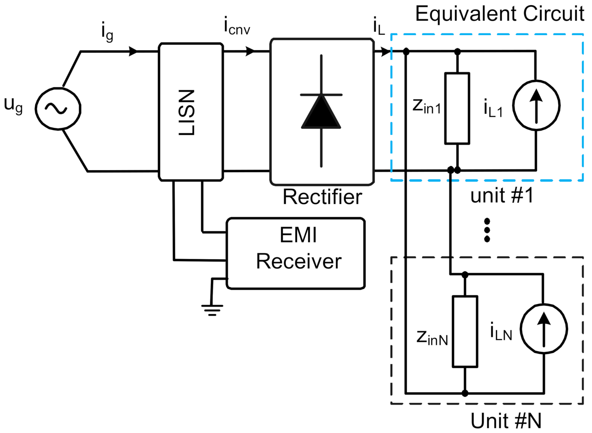
Only a few analytical-based approaches are introduced for differential mode noise as in [9] to EMI filter designing based on the input current ripple equation of the interleaved boost PFC. It is only suitable for EMI filter designing for conventional phase shift interleaved and frequency above 150 kHz. Analytical DM EMI estimation is proposed for non-interleaved PFC in [10] for Band-A. However, there are no fundamental studies despite reported EMI noise issues to estimate the EMI level for interleaved boost PFC based on the phase shift’s dependency, which can be investigated to minimize the DM EMI noise. Hence, this article suggests an analytical-based modeling approach for differential mode EMI noise estimation. The analytical model is proposed for an interleaved boost PFC converter, depicted in Figure 1 with including the impedance stabilizing network (LISN), EMI receiver, and EMI filter. To create the possibility of compliance with measuring all EMI measuring equipment’s impact, including the EMI receivers, LISN is also considered on the analytical model.
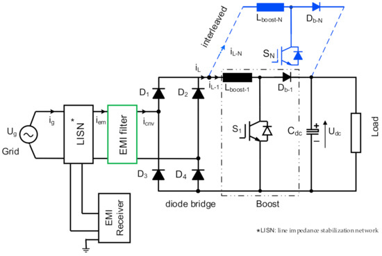
Figure 1.
Block diagram of an interleaved boost power factor correction (PFC) converter including impedance stabilizing network (LISN), electromagnetic interference (EMI) receiver, and EMI filter.
From an EMI viewpoint, finding the appropriate phase shift angles is of great importance to get an optimal filter volume [1,11]. So, the optimal DM EMI filters design for interleaved boost PFC applications is an important challenge, especially within the low-frequency EMI range in-between 2 and 150 kHz. This research’s primary purposes are to propose an appropriate analytical DM EMI noise estimation and EMI filter volume investigation. Moreover, the analytical noise estimation approach covers the number of interleaved units and the related different types of phase shifts. Thus, the unconventional phase shift is achieved based on the analytical EMI estimations for carrier harmonics on Band-B. Further, the effects of the different types of the phase shift on Band B and A DM EMI filter design have been investigated.
The main contributions of this research can be highlighted as follows. First, the impact of switching frequency selection and the number of interleaved stages in a single-phase PFC on DM EMI filter sizing (filter corner frequency and required attenuation) are analytically investigated. Second, an analytical method is proposed for interleaved PFC to predict maximum peak noise that is highly important in the DM EMI filter design. The dependency of the maximum peak noise on the phase shift between the interleaved units leads to the investigation of the phase shift impact on the DM EMI filter size via the EMI estimation approach. So, a novel formulation is presented for the unconventional phase shift method based on the EMI estimation analysis within Band B. Furthermore, it is shown that the unconventional phase-shift angle can be obtained depending on the switching frequency of the power converter and the number of interleaved stages. Third, a general flowchart is presented to find optimal filter volume based on the proper phase shift, EMI estimation approach, type of the band frequency, and volumetric component parameter.
The rest of the research is organized as follows. Section 2 details the design process of a typical two-stage DM EMI filter. In this section, the EMI measurement setup is described according to the CISPR standard such as EMI receiver and line impedance stabilizing network (LISN). Section 3 provides the process of getting the filter’s attenuation requirement and filters corner frequency in the interleaving units. In order to calculate the required filter attenuation, the simplified analytical modeling approach is presented in order to estimate DM EMI noise level in Section 4. Subsequently, in Section 5, the advantages of the unconventional phase shift in the interleaved units are developed in Band-B, where the filter attenuation drop is presented. Moreover, filter volume optimization is given based on the type of phase shifts in Section 6. Section 7 provides the experimental results of two interleaved boost PFC converters to validate the DM EMI model noise for different phase shifts. Ultimately, conclusions are provided in Section 8.
2. The Design Approached Two-Stage DM Filter
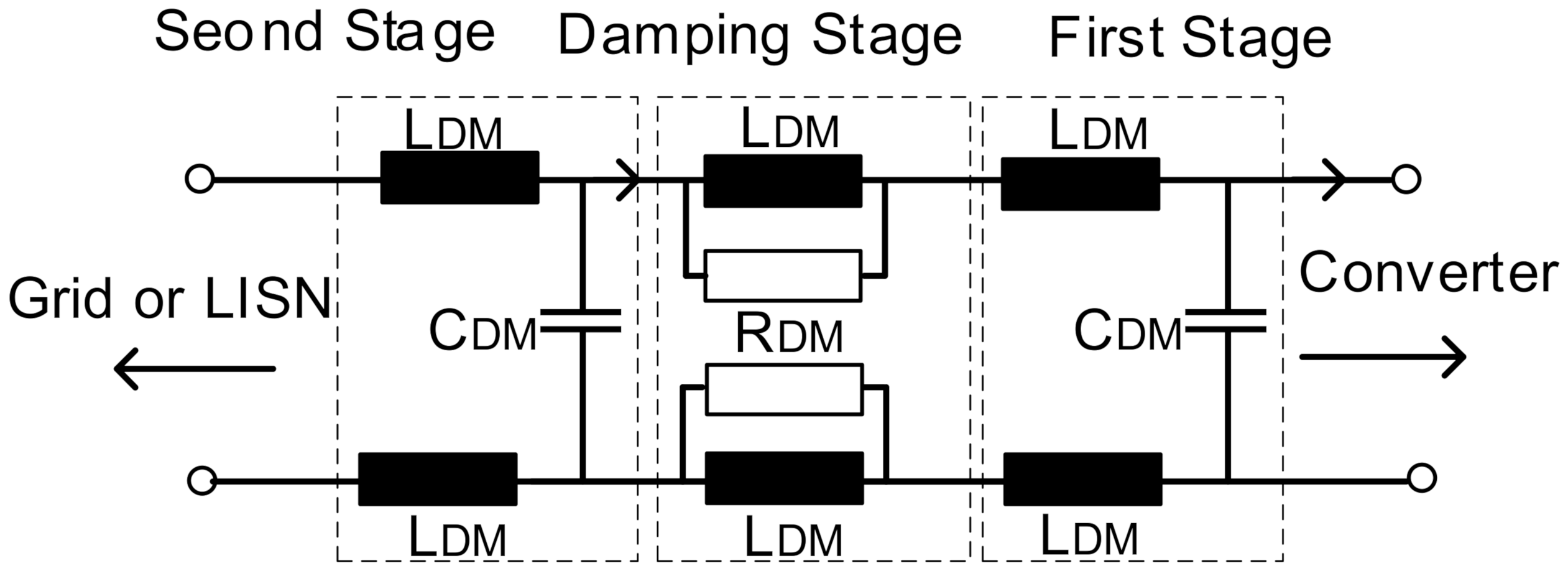
The EMI filter is employed for protecting the utility against the high frequency conducted emission noises. To this end, they should comply with EMI standard requirements. Therefore, a symmetrical two-stage filter structure design, as shown in Figure 2, is considered. Notably, the primary purpose of the EMI filter is to reduce the emission noise in order to fulfill relevant standards [3,5]. The selection of the filter components depends upon the filter attenuation requirement Att-req, calculated by (1) [6]:
where fD is filter design frequency, Umax is the first noise voltage peak. Att-req is the noise quantity, which should be damped by the filters. CISPRlimit is considered emission limits following CISPR-15 [5] and CISPR-11 [3] based on QP (Quasi Peak) for band A and B, respectively. Moreover, “Margin” is the filter design margin. It is considered as 6 dB because of uncertainty and EMI filter parameter tolerances [11,12,13]. Uncertainty is explicitly considered by establishing proper control procedures and characteristics of the production materials. In [14], the performance of novel control techniques for imperfect systems was studied. The procedure is based on the utilization of the unavoidable imperfections related to physical realizations. In addition, Att-req for a symmetrical two-stage EMI filter, including inductor and capacitor size is obtained by (2):

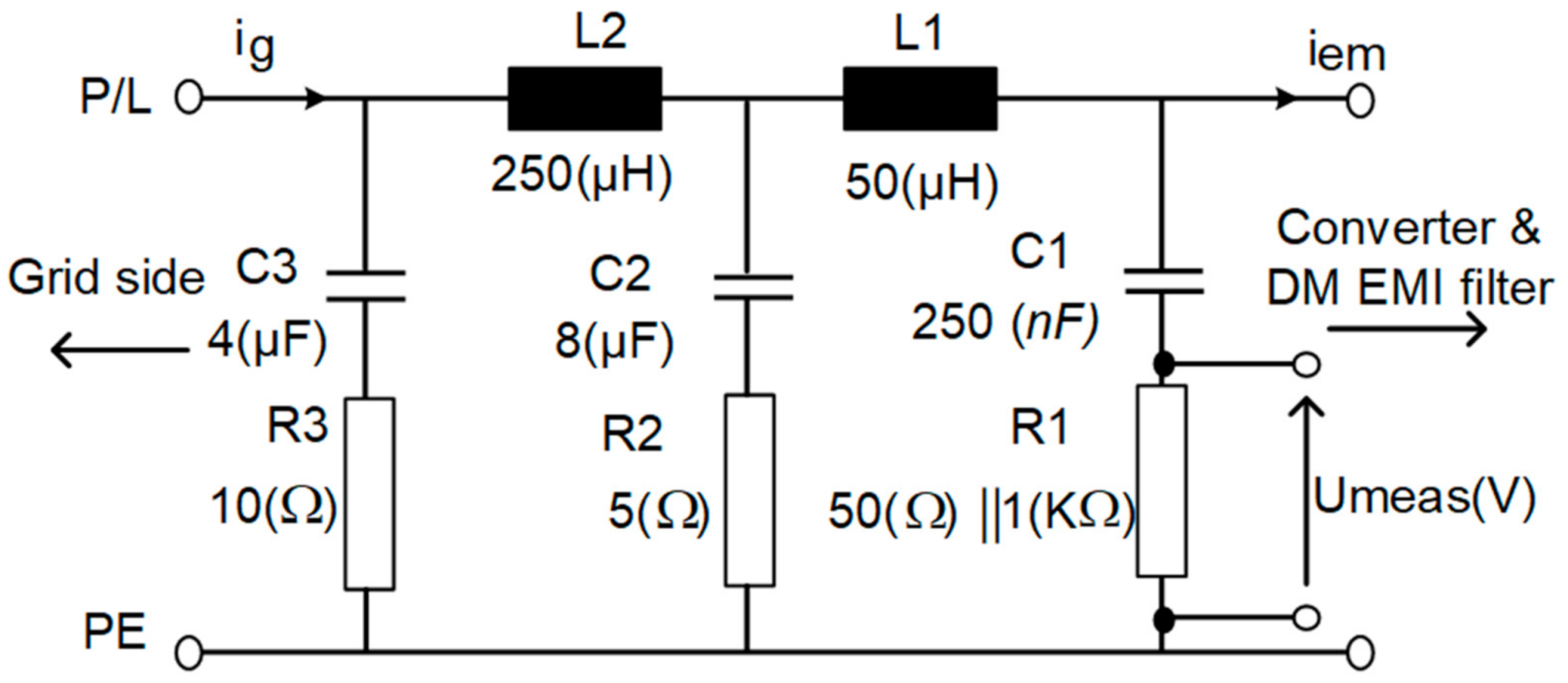
Figure 2.
Symmetrical two-stage differential mode (DM) EMI filter configuration.
As discussed earlier, the input ripple current reduction implies a lower DM EMI noise magnitude (Umax), and thus a smaller component size of the DM EMI filter. Additionally, the dependency of EMI filter corner frequency on the filter component results in a challenge in sizing the filter components. Accordingly, reducing the EMI filter component size makes the DM filter corner frequency higher. One of the primary goals of this research is to get an optimal corner frequency based upon the interleaved technique and the employed phase shift. The filter corner frequency is obtained by (3)
Moreover, to measure the Umax based on the CISPR-16 [11] standard requirement, a LISN and an EMI receiver are required. The LISN not only decouples the line and the device under test (DUT) but also provides an interface between the DUT and the test receiver. The LISN structure employed for EMI measurement within the frequency range of 9 kHz—30 MHz is illustrated in Figure 3. Notably, LISN is able to measure the RMS time-domain voltage (umeas) in order to define the EMI noise based on Equation (4). So, the EMI test receiver utilizes a QP detection to get the EMI peak measurement. Finally, by considering (4), the EMI peak measurement [13,15] is achieved:
where MB is frequency sweep that is shifted over the frequency band of interest. RBW is fourth order Butterworth bandpass filter, and the bandwidth (BW) is 200 Hz for Band A (9–150 kHz), and 9 kHz for Band B (150 kHz–30 MHz).
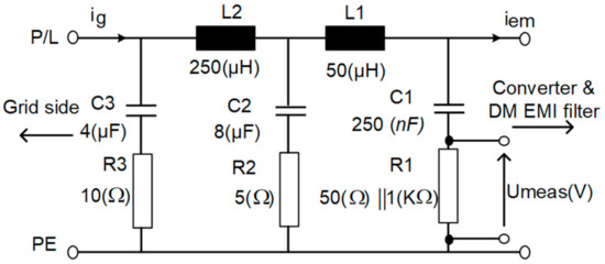
Figure 3.
LISN per-phase circuit diagram recommendation by CISPR-16 for 9–500 kHz [9,10].
3. Required EMI filter Attenuation in Interleaving Units Using Conventional Phase Shift
The interleaved boost PFC and the related advantages have been reported in the past literature [1]. Here, Figure 1 illustrates the block-diagram of the test system, including two interleaved boost PFCs, EMI receiver, LISN and EMI filter, and the boost-inductor design for continuous conduction mode (CCM) [16,17] operation has already provided in the literature. So, for the simplicity, only the widely used equations are specified in this subsection, and the boost inductor size for CCM operations is obtained by (5) assuming 22% input ripple current according to [18]:
The value of parameters for a single-phase PFC are summarized in Table 1. The parameters are used to define the filter’s attenuation requirements with respect to various switching frequencies in CCM. So, inductor size, as presented in Table 2, can be obtained via (5) for the different case studies. Thus, the maximum peak values of the spectrum (Umax) for various frequency switchings are achieved based on PLECS simulations and Equation (4). Figure 4 illustrates the phase shift implementation between the two units with phase shift 180° in order to decrease input ripple currents on the boost stages. Notably, as shown in Figure 4, selecting the proper phase shift may affect the ripple of input current. Providing numerous simulation case studies with different phase shifts and switching frequencies is a time-consuming and complicated task at the system-level analysis. In order to alleviate the computational burden/time, a new analytical estimation is proposed in Section 5. In this section, the interleaving technique is evaluated to get the optimal design of DM EMI filter. So, up to four interleaved units have been working at different switching frequencies in Band A and Band B to get the connection between the attenuation requirement considering the interleaving and phase shifting. So, the conventional phase shift of 360°/N (N is the number of the interleaved converters) is employed among the interleaved units. Interestingly, the first noise peak value erects at the switching frequency of fsw in Band B. By interleaving task, the equivalent switching frequency is equal to N fsw, where N denotes the number of the interleaved units. More details about the impact of the interleaving task on ripple current has been reported in [1].

Table 1.
Case Study Specification of Single-Phase Boost PFC.
Table 2.
Inductor Sizes For Single-Phase Unit In continuous conduction mode (CCM) Modes based On (5).
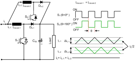
Figure 4.
Analysis phase shift effects on input ripple current in two units interleaved boost stages. The phase shift between units is considered 180°.
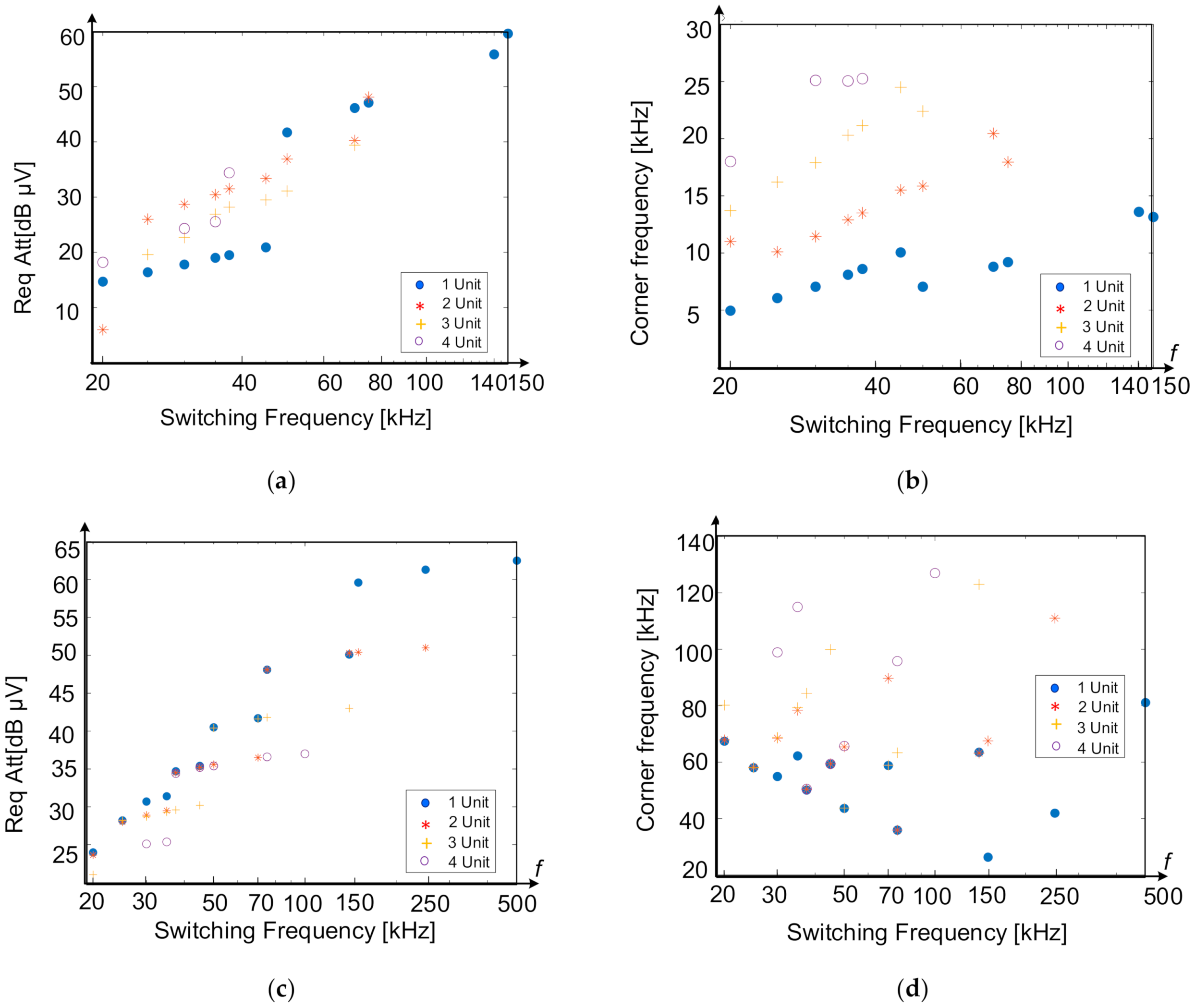
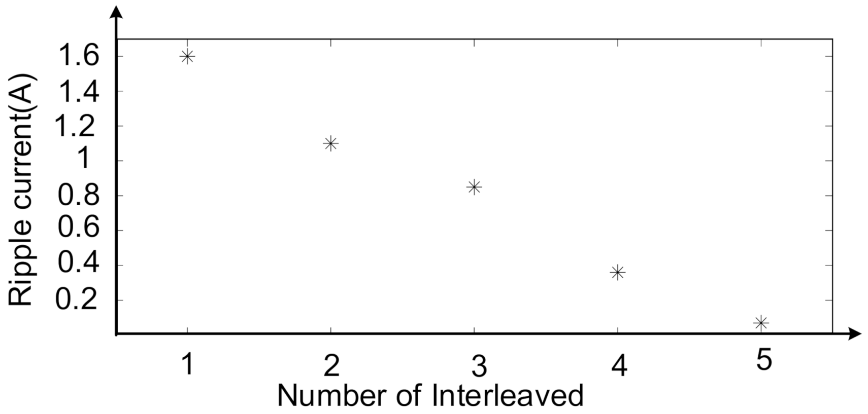
Figure 5a depicts the connection between the attenuation requirement and the switching frequency up to four units for CCM mode in Band A. As the equivalent switching frequency appears in N fsw, thus there is no need to employ a filter if the switching frequency is considered higher than 75 kHz in two units, 50 kHz in three units, and 37.5 kHz in four units. Further, Figure 5b depicts the filter corner frequency (fc) via different switching frequencies for a two-stage DM EMI filter in Band A subjected to (1)–(2). Notably, as depicted in Figure 5c,d, the filter corner frequency increases while the filter attenuation requirement decreases at a specific switching frequency range (30–37.5 kHz, 50–75 kHz, and >150 kHz) in two units interleaved. For example, in order to select switching frequencies of 35 kHz and 30 kHz in Band B, filter design frequencies appear at 175 kHz and 150 kHz, respectively (fifth carrier harmonics occur above 150 kHz). Hence, a case study with 175 kHz compared with 150 kHz obtains a smaller component size and higher filter corner frequency in the same filter attenuation requirement. Thus, switching at the aforementioned critical frequencies and utilizing a switching frequency lower than them is not highly efficient. Because this increases the filter corner frequency without affecting the boost inductor size. In addition, using the interleaving technique leads to decreased input ripple currents. Hence, Figure 6 shows the relationship between the input ripple current with the number of the interleaved converter using PLECS simulations. The current ripple decreases by adding the number of interleaved units. From the ripple current perspective, it is not beneficial to increase the number of units above 5.
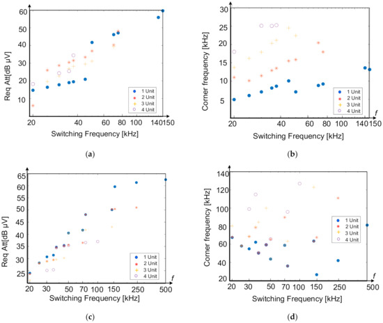
Figure 5.
Relationship between attenuation requirement and the switching frequency (up to four units interleaved) in (a) Band A. (c) Band-B. The relationship between a two-stage filter corner frequency and switching frequency (up to four units interleaved) in (b) Band A (d) Band B for CCM based on the attenuation requirement (1)–(2). The conventional phase shift is considered 360°/N.

Figure 6.
Input ripple current on the basis of the number of the interleaved converters with fsw = 37.5 kHz, P0 = 1 kW, and Lboost =1 mH based on PLECS simulations.
4. Proposed DM EMI Estimation Method for Interleaved Units
In this part, time-frequency analytical modeling methods are used for DM EMI noise prediction that is important in the DM EMI filter design in order to fulfill the standard requirements. Additionally, the proposed method is on the basis of the closed-loop input impedance and the double Fourier analysis of the noise source spectrum. The suggested technique characterizes the production emissions of the power converter within the frequency range of 9–500 kHz considering the double Fourier analysis and closed-loop impedance. Extra details about the modeling of DM noise, closed-loop input impedance, and the frequency behavior have been reported in [10] for single-phase non-interleaved boost PFC. The DM noise spectrum of each switch is presented by (6), where it contains a DC offset value, baseband harmonics, carrier group harmonics, as well as sideband harmonics [19]:
where m and n denote the carrier group and baseband group indexes, respectively. The fundamental and carrier angular frequencies are denoted by closed-loop and w0. A0n, B0n, Am0, Bm0, Amn, and Bmn denote the harmonic coefficients [10,19]. Moreover, it has to be noted that the carrier harmonics can be updated by the phase shift effects given as (7):
Finally, sideband harmonics are obtained by the phase shift effects in interleaved units given as (8):
where θ is an interleaved unit phase shift, which can be selected by the phase selecting methods. For instance, in two interleaved units, the first unit phase shift is zero, and the second unit phase shift is θ. The structure of a simplified case study with a Norton equivalent circuit is illustrated in Figure 7. The current for N units can be calculated from (9):
where (n’−1) θ is the phase shift for unit number n’. The PFC converter’s input impedance based on a large signal model is obtained by (10) [10]:
where umo denotes the peak-to-peak value of the PWM signal, and g denotes a constant value. More details on the closed-loop impedance modeling of the boost PFC converter are reported in [20]. Since the switching function of the diode rectifier is a square-waved signal, its Fourier transform is obtained by (11):
where h is harmonics order number. Thereby, the LISN input current without EMI filter is obtained by (12):
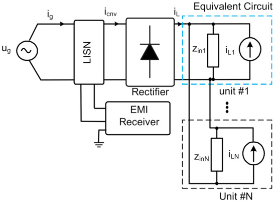
Figure 7.
Norton equivalent circuit of the interleaved boost PFC converter.
The relationship between the LISN input current and EMI receiver voltage should be added in the proposed analytical method to complete it. Hence, the relationship between the input current LISN and EMI receiver branch by considering the EMI filter is given as (13) [10]:
C and D are defined in Equations (14) and (15), [10] as
In addition, the EMI receiver voltage noise is
5. Unconventional Phase Shift Approach
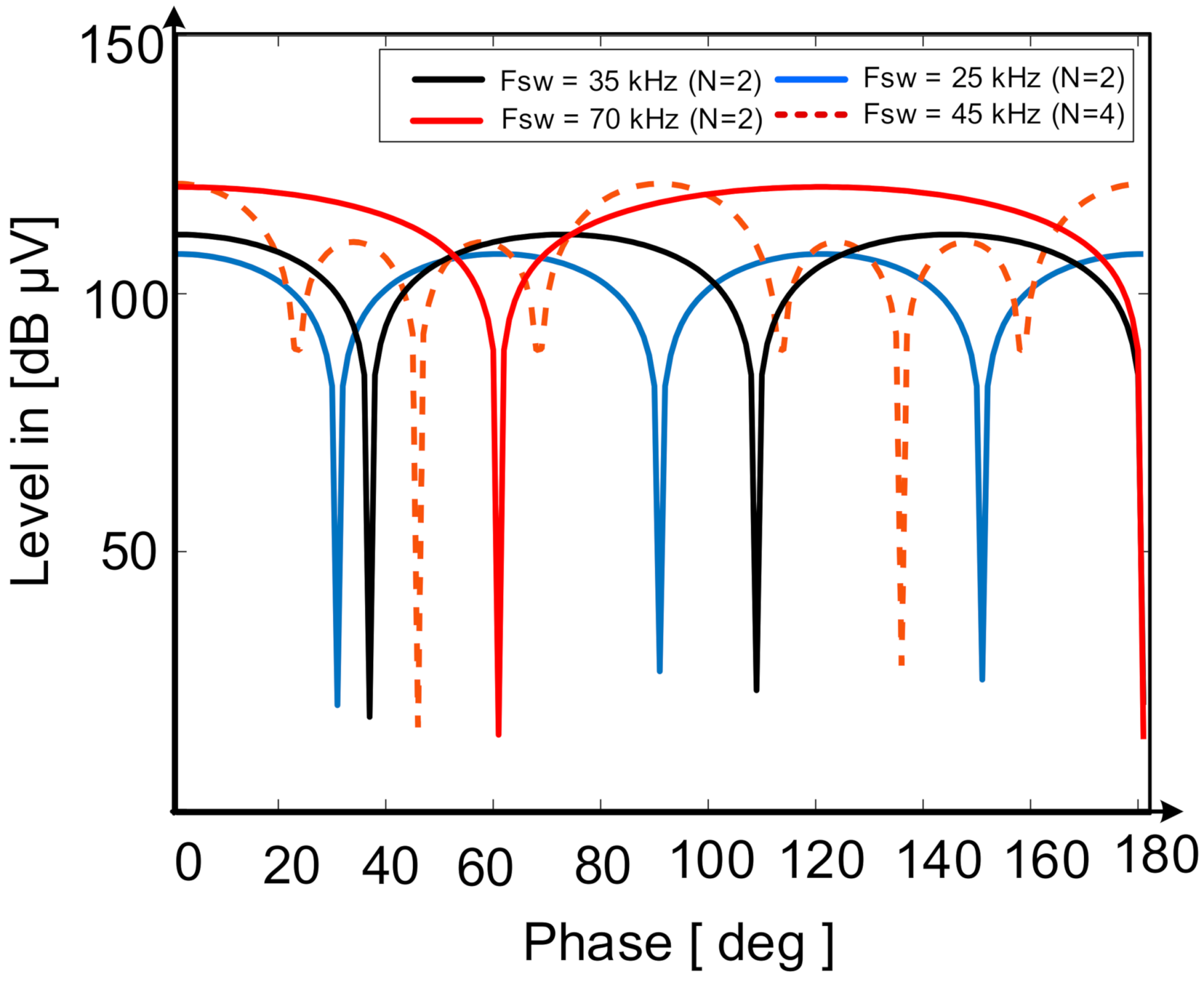
As seen in Figure 5c, the attenuation requirement and filter corner frequency are slightly different for one unit non-interleaved and two units and three units with a conventional phase shift. Hence, the interleaving technique does not have any benefits at some switching frequency ranges, such as 75–150 kHz, for two units interleaved in comparison to one unit in Band B. Hence, observing the carrier frequency harmonics behavior based on the phase to get the unconventional phase shift is essential in that frequency range. Notably, analytical EMI estimation can be predicted on EMI noise level in any order of carrier frequency harmonics based on the selective phase angle. Therefore, an unconventional phase shift can be selected by looking at the first appeared carrier harmonics behavior in the different phases in Band B. Hence, Table 3 provides an unconventional phase shift from an analytical estimation approach to get a low filter attenuation requirement based on the switching frequency and the number of interleaved units. Figure 8 depicts the first carrier harmonics behavior in Band B for several interleaved case studies in different phases and switching frequencies. The first carrier harmonics can be removed by proper phase shift selection. On the other hand, by eliminating the first noise peak, which is important in EMI filter design in Band B, the filter design frequency shifts to a high frequency. So, (17) and (18) representing unconventional phase shift formulation are obtained from Table 3 by assessing the relation between N, k, and θ.
where k denotes the harmonic order of the switching frequency, that is the first noise peak in Band B.
Table 3.
The Unconventional Phase Shift Angles at the Switching Frequency Range (20–150 kHz) up to Four Units Interleaved for Band B.
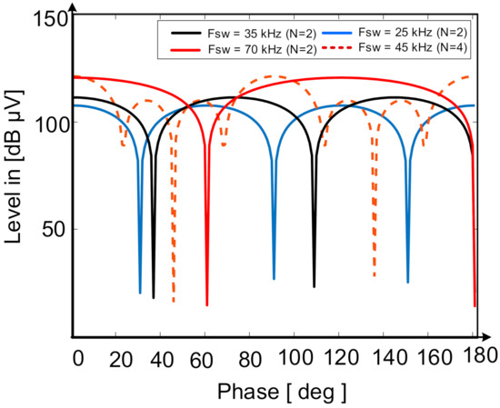
Figure 8.
First carrier harmonics behavior with various switching frequencies in Band-B for three interleaved units with different phases.
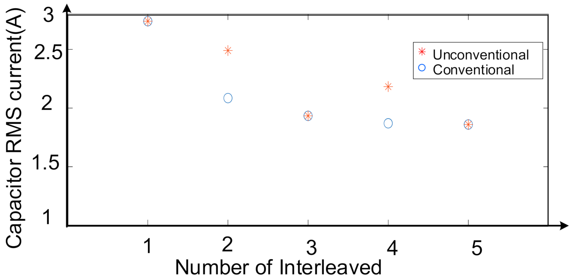
Notably, unconventional phase shift does not affect the DM EMI filter loss. Since the DM capacitor takes most of the switching ripple, the DM inductor loss is almost the same no matter which phase shift is applied. In addition, Figure 9 illustrates the RMS input current of the DC-link capacitor for conventional phase shift and unconventional phase shift based on the number of the interleaved converters. As it is clear from Figure 9, the unconventional phase shift increases the RMS capacitor input current in some cases. Notably, it does not affect the DC capacitor size regarding ripple current is lower than non-interleaved PFC.
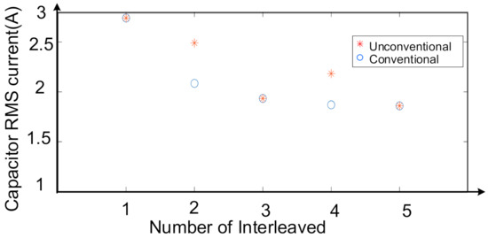
Figure 9.
Input ripple current of the DC capacitor on the basis of the number of the interleaved converters with fsw = 37.5 kHz, P0 = 1 kW, and Lboost = 1 mH based on PLECS software simulations. The conventional phase shift is considered 360°/N and unconventional is selected based on the (17) and (18).
6. Filter Volume Optimization
In this section, the primary purpose is to optimize the EMI filter size considering the selected proper phase shift. To investigate the efficiency of the proposed method, EMI filter volume can be calculated based on [15]. As mentioned above, the symmetrical two-stage EMI filter [18], shown in Figure 2, has been considered for this paper’s analysis. Hence, the EMI filter capacitor size can be obtained from (19) [15]:
where the factor kC1 denotes the capacitor volume proportionality to the stored energy and kC2 denotes a voltage-dependent factor. Furthermore, the inductor size is obtained by (20) [15]:
kL1 is a constant factor describing the proportionality between the stored energy EL = 1/2·LDM·Ig2 and the inductor volume. These factors can be derived analogously to kL1, kL2, and kL3 from the manufacturer’s data using Magnetics toroid cores [10], which is present in Table 1. So, the total volume of the two-stage symmetrical EMI filter is calculated from (21):
where nf is the number of filter stages [9,15,18]. Solving (19)–(21) and (2) results in optimum filter component parameters for a certain number of filter stages nf. To simplify the calculation analysis, (2) is simplified for two-stage EMI filter as
Finally, EMI filter components are calculated by
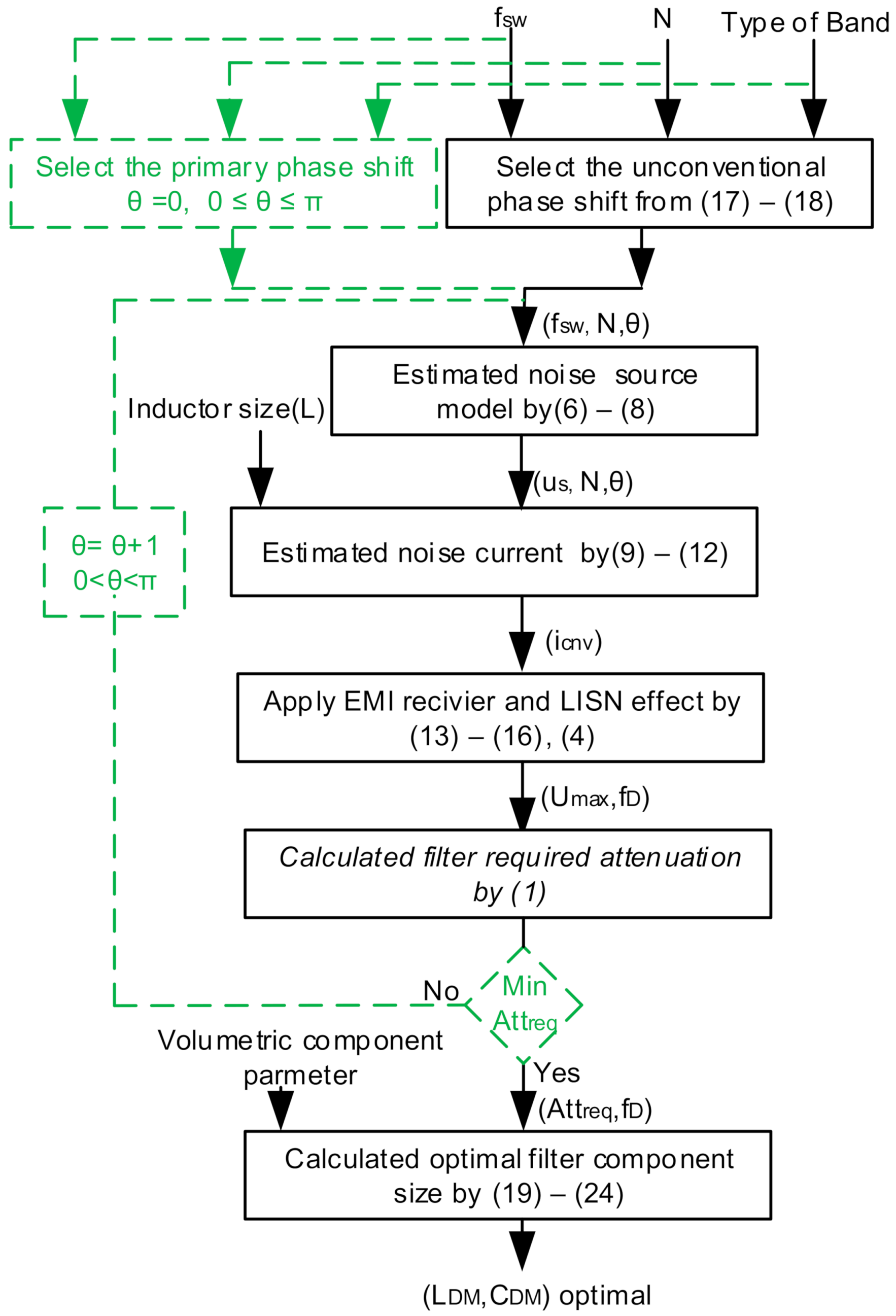
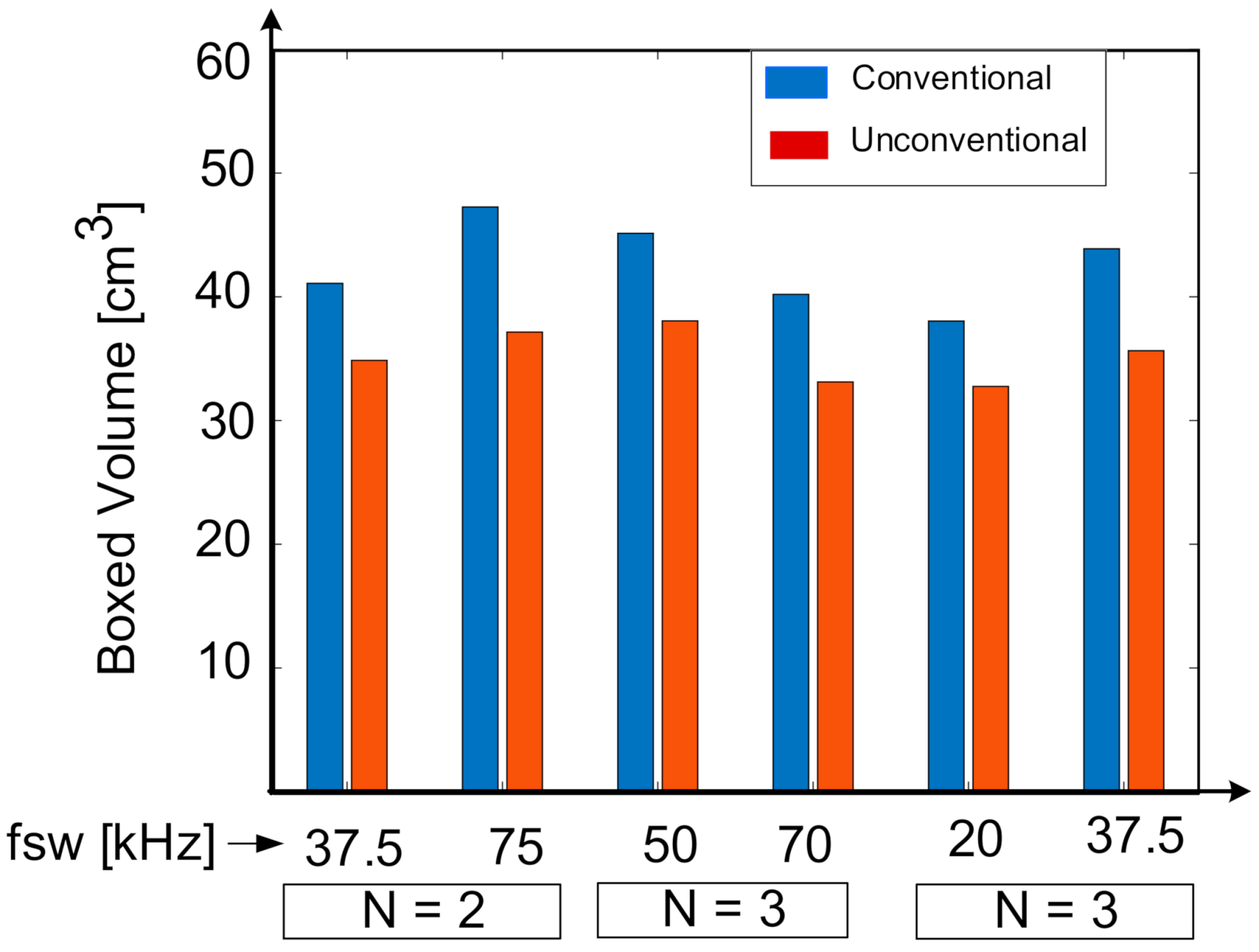
Finally, Figure 10 shows a flowchart demonstrating the steps to design the optimal filter volume based on the analytical EMI noise estimation approach. Further, as it is clear from Figure 8, the relation (17)–(18) does cover some unconventional phase angles that filter required attenuation minimized from the analytical method. On the other hand, there are other points for minimization filter required attenuation. The green dash line in Figure 10 shows the general method for phase shift selection based on the analytical estimation. Moreover, (17)–(18) can use instead of the general unconventional phase-shifting method to improve computation time. This flowchart is mainly applied to calculate the EMI filter component with only a few equations considering proper phase shifts with unconventional phase shift or analytical estimation. Hence, Figure 11 shows optimal DM EMI filter boxed-volume approximation, including conventional and unconventional phase shifts in Band-B based on Table 3 and Figure 10. As previously mentioned, the unconventional phase shift efficiency in a decreased EMI filter size is obtained from Figure 11. Here, two cases are presented with different phase shifts, including conventional as 180° and unconventional as 45° selected from Table 3 based on the fsw = 37.5 kHz for two units interleaved.

Figure 10.
Flow chart of DM EMI filter boxed-volume optimization.
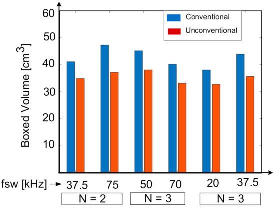
Table 4 provides the outcome of the two case studies, including the attenuation requirement and corner frequency. The phase shift of 45° compared to 180° is required for a lower filter attenuation in Band B, while a phase shift of 180° needs a higher filter attenuation. As it is clear from Table 4, the unconventional and conventional phase shifts provide many beneficiaries such as EMI filter size reduction in Band B and Band A, respectively. Notably, Figure 12 is shown the proposed flowchart optimization approach for EMI filter designing and its benefit to fulfill the EMI level under the standard limitation in designing band frequency.
Table 4.
Band-B and A EMI Filter Design Based on PLECS Simulations for conventional (180°) and unconventional Phase Shift (45°) regarding (17) And (18). The Switching Frequency is 37.5 kHz For Two Interleaved Units.
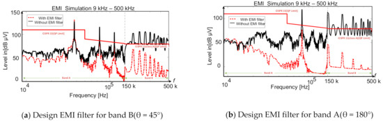
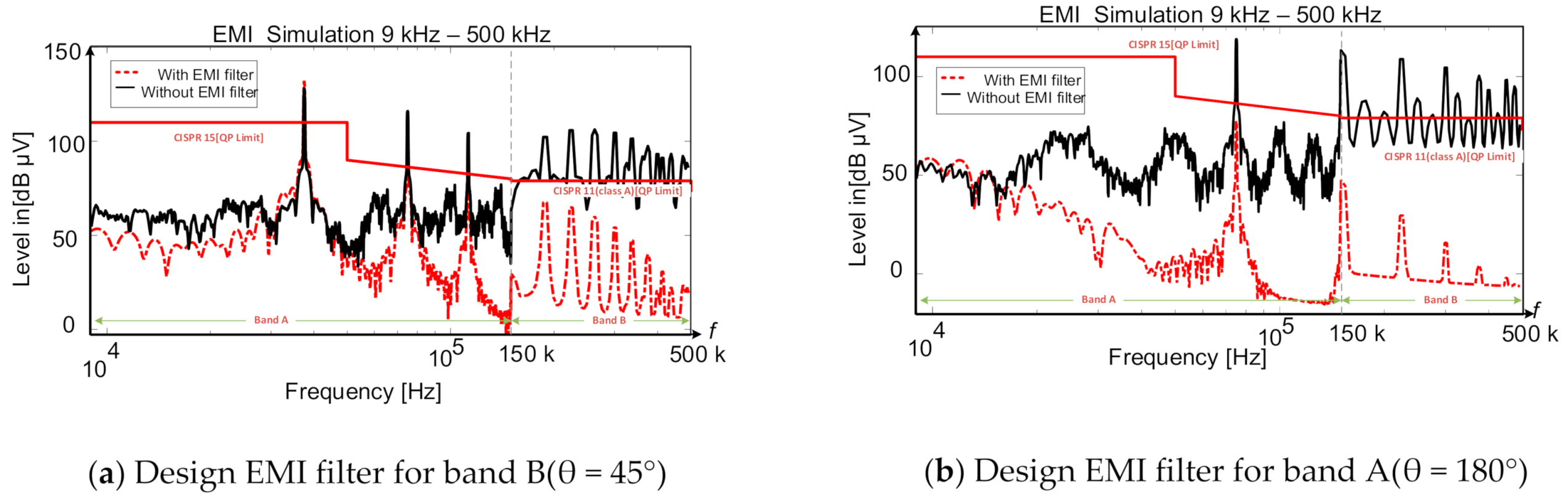
Figure 12.
EMI simulation approach for two-unit interleaved CCM at fsw = 37.5 kHz based on Table 4.
7. Experimental Results
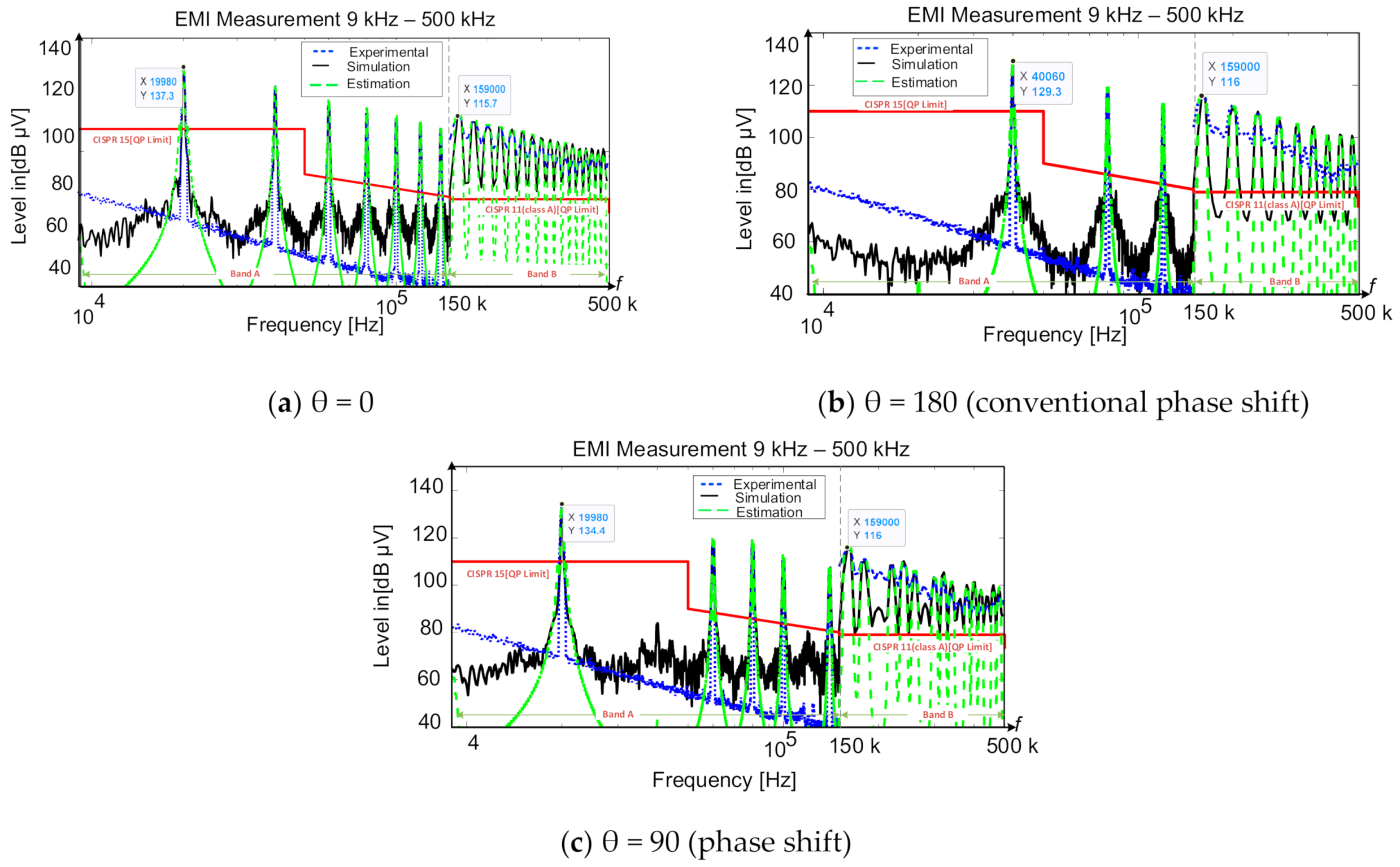
In order to validate the theoretical analyses, a two-unit interleaved boost PFC rectifier, depicted in Figure 1, operating in CCM is taken into account. The required data are summarized in Table 5. A laboratory setup, including EMI receiver, LISN, and the two-unit interleaved converter is considered to validate theory and design. A simplified prototype of the single-phase interleaved boost PFC converter, illustrated in Figure 13, is utilized to verify the proposed method. In addition, the simulation model is carried out in PLECS. The sampling frequency for simulations and experiments is 100 kHz, and Figure 14 depicts the experimental waveforms of two units—interleaved through the parameters (fsw = 20 kHz) and phase shift 180° given in Table 5. The first test case is a two-unit interleaved PFC with a zero-phase shift. Figure 15a compares the simulation and experimental results for two-unit interleaved with θ = 0°. The purpose of employing the phase-shifting technique is to suppress the harmonics. As there is no cancelation impact for the θ = 0°, it can be simply used as an acceptable case scenario for filter’s attenuation requirement. In the second test, a 180° phase difference between two interleaved PFC is applied which is called interleaving using a conventional phase shift. It is obvious from Figure 15b that the experimental results are verified via simulations by the conventional phase shift between the units. Notably, the first order of harmonics appears in 2fsw compared to θ = 180° at higher frequencies. It has many benefits on Band A, including the elimination of the odd order noises, and it is shifting the EMI filter design frequency to a higher frequency. Therefore, the filter size decreases as it occurs at a high frequency.
Table 5.
Case Study Specification.

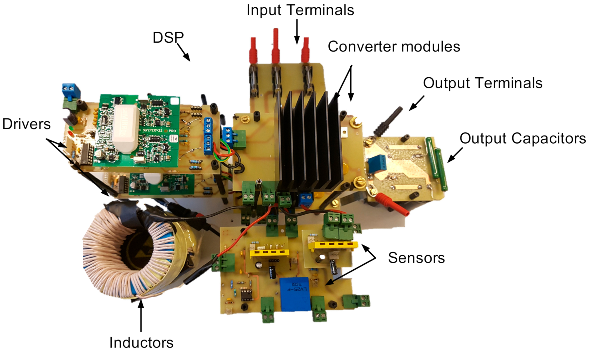
Figure 13.
Experimental prototype of two single phase interleaved boost PFC converter.

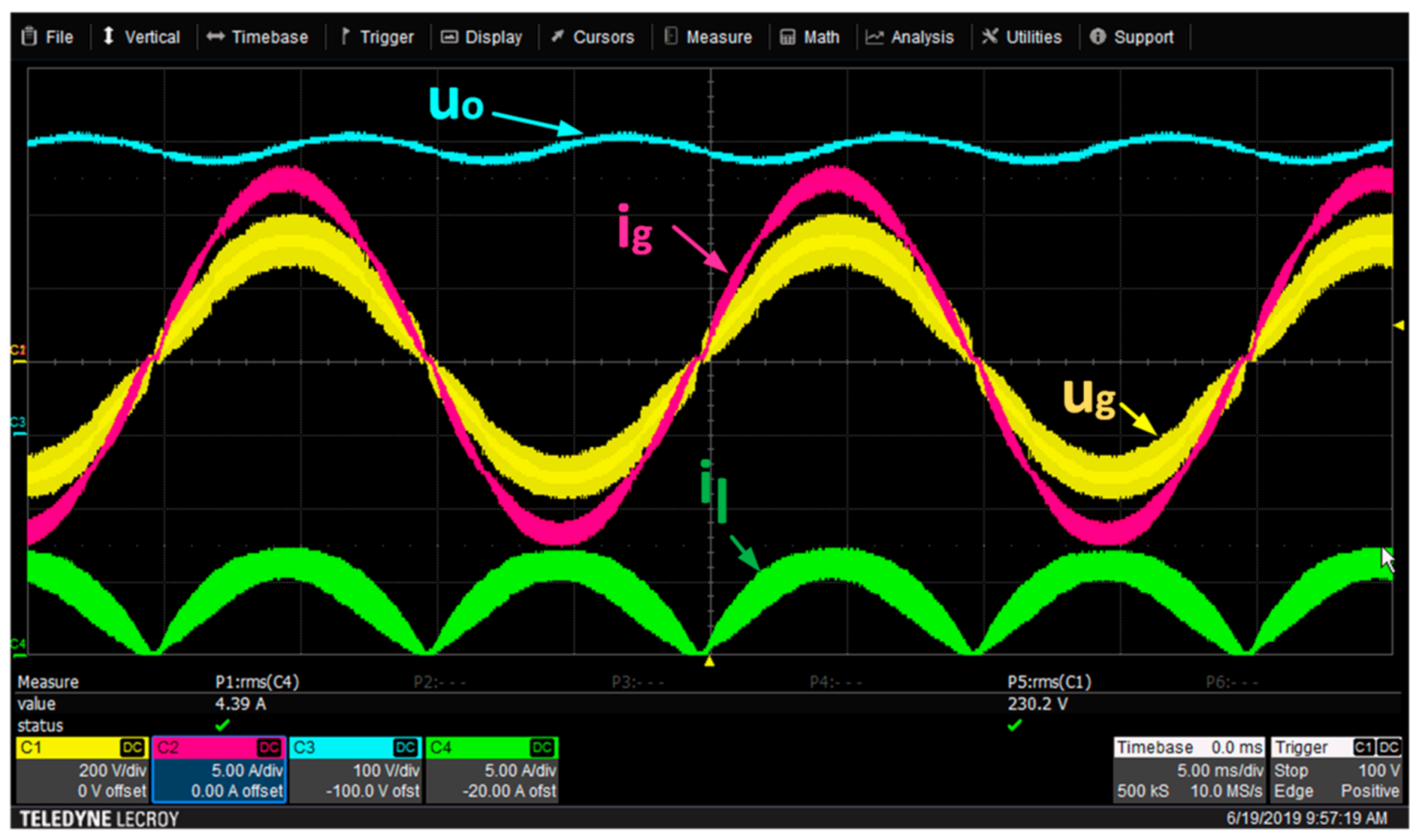
Figure 14.
Measured waveforms of two units interleaved using parameters (fsw = 20 kHz) and a phase shift of 180° given in Table 5.
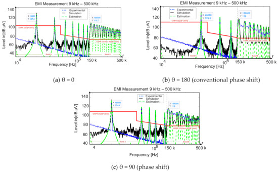
Figure 15.
EMI results measurement for 2-unit interleaved boost PFC converter, including estimation-based proposed model, simulations, and experiments for different phase shift including (a) 0°, (b) 180°, and (c) 90°. Test system specification is on the basis of results given in Table 5.
The second part of the experiments is related to the selective unconventional phase shift. As mentioned before, the second order harmonics disappear when 90° is considered as a phase shift. This scenario illustrates the effect of 90° as a phase shift if the switching frequency is selected to be 75–150 kHz. Hence, the second-order harmonics appear to be above 150 kHz, and by using the 90° as a phase shift, it can remove the second harmonics, which is the first harmonic in Band B. Since the switching frequency limitation of the test setup, the effect of this phase shift is investigated at 20 kHz. On the other hand, Figure 15c is shown the effects of the 90° phase shift on the second harmonics cancelation. Hence, Figure 15c shows the unconventional phase shift impacts considering 90° as a phase shift between the units for two-unit interleaved. As the noise-emission level is quite above the standard requirements, as depicted in Figure 15, designing an appropriate EMI filter is necessary. Further, Figure 15 depicts the simplified estimated DM EMI approach for different phase shifts as the method estimates the DM EMI noise with an error lower than 1 dB in Band A and Band B. As the concentration of harmonics energy on the top of the harmonics is important, the results are just shown on the top of the harmonics’ multiple order. Hence, Table 6 summarizes the comparative DM noise results for one case study having different phase shifts for comparisons. Obviously, the proposed analytical model accurately matches the experimental results, and the maximum errors in Band A and Band B are below 1 dB for all considered phase shifts. This analytical modeling approach is valid for the different phase shifts, and also it can be applied by the many interleaved parts.
Table 6.
Comparative DM Noise Results for the Case Studies.
8. Conclusions
This research studied the impact of unconventional proposed phase-shift selection on EMI filter optimization for both Band A (9–150 kHz) and Band B (>150 kHz). The results obtained in Band A revealed that the interleaved topology provided has more advantages which gives the possibility of using no filter if the switching frequency is higher than 75 kHz for two units, 50 kHz for three units, and 37.5 kHz four units. Additionally, in Band-B, the application of conventional phase-shift between the units was not effective for all switching frequency ranges. Thus, various phase-shifts (unconventional) were employed to get a higher corner frequency and smaller filter size in Band B based on the EMI estimation technique.
Notably, in order to design a DM EMI filter, the proposed technique was used to model the noise level with higher accuracy at different phase shifts. In addition, this research highlighted the benefits of using the conventional phase shifts in Band-A to suppress the odd-order harmonics in order to optimize the attenuation requirement for EMI filter design. At the end, filter volume optimization was utilized to get a minimized component size by using an analytical estimation method and selective proper phase shifts. Therefore, a general method based on the analytical equation considering phase shift was employed to make EMI filter volume optimization. Experimental results verified the EMI estimation method with different phase shifts in Band A and Band B, and their maximum errors are below 1 dB.
Author Contributions
N.N.E. conceived and designed the paper and wrote the Introduction and Materials and Methods. Discussions and Conclusions were the collective work of all authors. The writing review and editing were performed by P.D., H.W., F.B. All authors have read and agreed to the published version of the manuscript.
Funding
This research received no external funding.
Institutional Review Board Statement
Not applicable.
Informed Consent Statement
Not applicable.
Data Availability Statement
The study did not report any data.
Conflicts of Interest
The authors declare no conflict of interest
References
- Wang, C.; Xu, M.; Lee, F.; Lu, B. EMI Study for the Interleaved Multi-Channel PFC. In Proceedings of the 2007 IEEE Power Electronics Specialists Conference, Orlando, FL, USA, 17–21 June 2007; pp. 1336–1342. [Google Scholar]
- Nussbaumer, C.; Raggl, K.; Kolar, J.-K. Design Guidelines for Interleaved Single-Phase Boost PFC Circuits. IEEE Trans. Ind. Electron. 2009, 56, 2559–2573. [Google Scholar] [CrossRef]
- CISPR. Limits and methods of measurement of Radio-frequency disturbance characteristics of Industrial, scientific and medical equipment-Publication 11. IEC Int. Spec. Comm. Radio Interf. 2015, 11, 192. [Google Scholar]
- CISPR. Electromagnetic compatibility—Requirements for household appliances, electric tools and similar apparatus—Part 1: Emission-Publication 14. IEC Int. Spec. Comm. Radio Interf. 2020, 14, 132. [Google Scholar]
- CISPR. Limits and methods of measurement of radio disturbance characteristics of electrical lighting and similar equipment Interference. IEC Int. Spec. Comm. Radio Interf. 2018, 15, 153. [Google Scholar]
- Hartmann, M.; Ertl, H.; Kolar, J.W. EMI Filter Design for a 1 MHz, 10 kW Three-Phase/Level PWM Rectifier. IEEE Trans. Power Electron. 2011, 26, 1192–1204. [Google Scholar] [CrossRef]
- Bishnoi, H.; Baisden, A.C.; Mattavelli, P.; Boroyevich, D. Analysis of EMI Terminal Modeling of Switched Power Converters. IEEE Trans. Power Electron. 2012, 27, 3924–3933. [Google Scholar] [CrossRef]
- Mehri, M.; Amini, A. Stochastic EMI Noise Model of PCB Layout for Circuit-Level Analysis of System in IoT Applications. IEEE Trans. Microw. Theory Tech. 2020, 68, 1. [Google Scholar] [CrossRef]
- Raggl, K.; Nussbaumer, T.; Kolar, J.W. Guideline for a Simplified Differential-Mode EMI Filter Design. IEEE Trans. Ind. Electron. 2009, 57, 1031–1040. [Google Scholar] [CrossRef]
- Nourani Esfetanaj, N.; Peyghami, S.; Wang, H.; Davari, P. Analytical Modeling of 9–150 kHz EMI in Single-Phase PFC Converter. In Proceedings of the IECON 2019—45th Annual Conference of the IEEE Industrial Electronics Society, Lisbon, Portugal, 14–17 October 2019; pp. 4689–4693. [Google Scholar]
- C.I.S.P.R. Specification for Radio Interference Measuring Apparatus and Measurement Methods, Publication 16. IEC Int. Spec. Comm. Radio Interf. 2019, 16, 195. [Google Scholar]
- Wang, C.; Xu, M.; Lee, F.C. Asymmetrical interleaving strategy for multi-channel PFC. In Proceedings of the Twenty-Third Annual IEEE Applied Power Electronics Conference and Exposition, Austin, TX, USA, 24–28 February 2008; pp. 1409–1415. [Google Scholar]
- Davari, P.; Blaabjerg, F.; Hoene, E.; Zare, F. Improving 9–150 kHz EMI Performance of Single-Phase PFC Rectifier. In Proceedings of the CIPS 2018 10th International Conference on Integrated Power Electronics Systems, Stuttgart, Germany, 20–22 March 2018; pp. 1–6. [Google Scholar]
- Bucolo, M.; Buscarino, A.; Famoso, C.; Fortuna, L.; Frasca, M. Control of imperfect dynamical systems. Nonlinear Dyn. 2019, 98, 2989–2999. [Google Scholar] [CrossRef]
- Raggl, K.; Nussbaumer, T.; Kolar, J.W. Model based optimization of EMC input filters. In Proceedings of the 2008 11th Workshop on Control and Modeling for Power Electronics, Zurich, Switzerland, 17–20 August 2008; pp. 1–6. [Google Scholar]
- Luo, H.; Xu, J.; He, D.; Sha, J. Pulse Train Control Strategy for CCM Boost PFC Converter with Improved Dynamic Response and Unity Power Factor. IEEE Trans. Ind. Electron. 2020, 67, 10377–10387. [Google Scholar] [CrossRef]
- Davari, P.; Zare, F.; Abdelhakim, A. Active Rectifiers and Their Control, Control of Power Electronic Converters and Systems (Editor Frede Blaabjerg); Elsevier: Amsterdam, The Netherlands, 2018; pp. 3–52. [Google Scholar]
- Raggl, K.; Nussbaumer, T.; Doerig, G.; Biela, J.; Kolar, J.W. Comprehensive Design and Optimization of a High-Power-Density Single-Phase Boost PFC. IEEE Trans. Ind. Electron. 2009, 56, 2574–2587. [Google Scholar] [CrossRef]
- Holmes, D.G.; Lipo, T.A. Pulse Width Modulation for Power Converters: Principles and Practice; IEEE Press-Wiley: Piscataway, NJ, USA, 2003; p. 744. [Google Scholar]
- Sun, J. Input Impedance Analysis of Single-Phase PFC Converters. IEEE Trans. Power Electron. 2005, 20, 308–314. [Google Scholar] [CrossRef]
Publisher’s Note: MDPI stays neutral with regard to jurisdictional claims in published maps and institutional affiliations. |
© 2021 by the authors. Licensee MDPI, Basel, Switzerland. This article is an open access article distributed under the terms and conditions of the Creative Commons Attribution (CC BY) license (http://creativecommons.org/licenses/by/4.0/).