
A Compact Rectifier Design Method Utilizing Harmonics

Abstract
1. Introduction
2. Design and Simulation
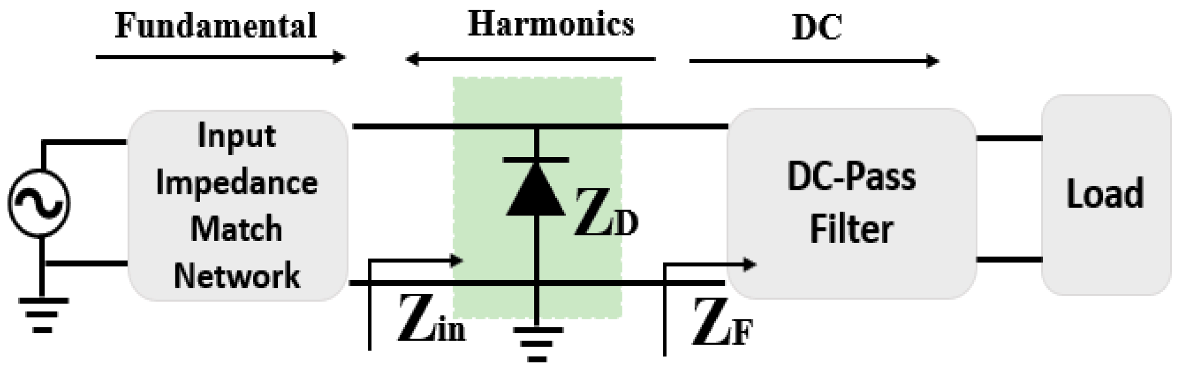
2.1. Principle
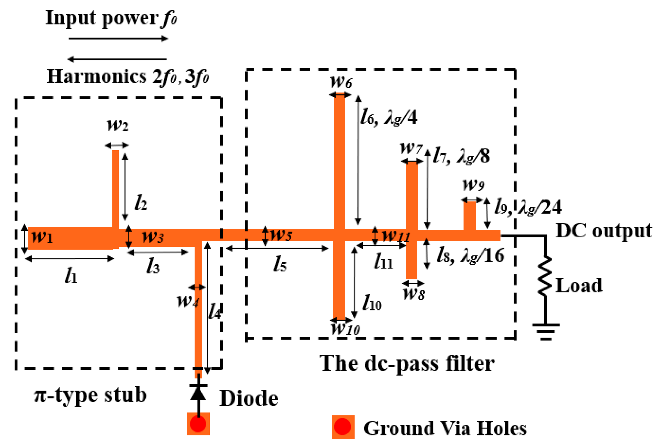
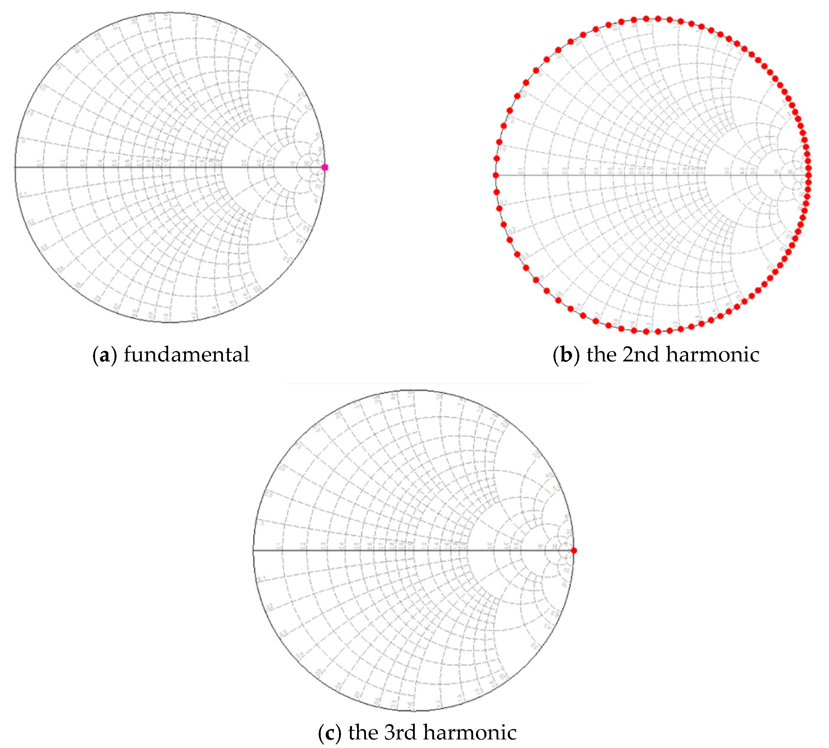
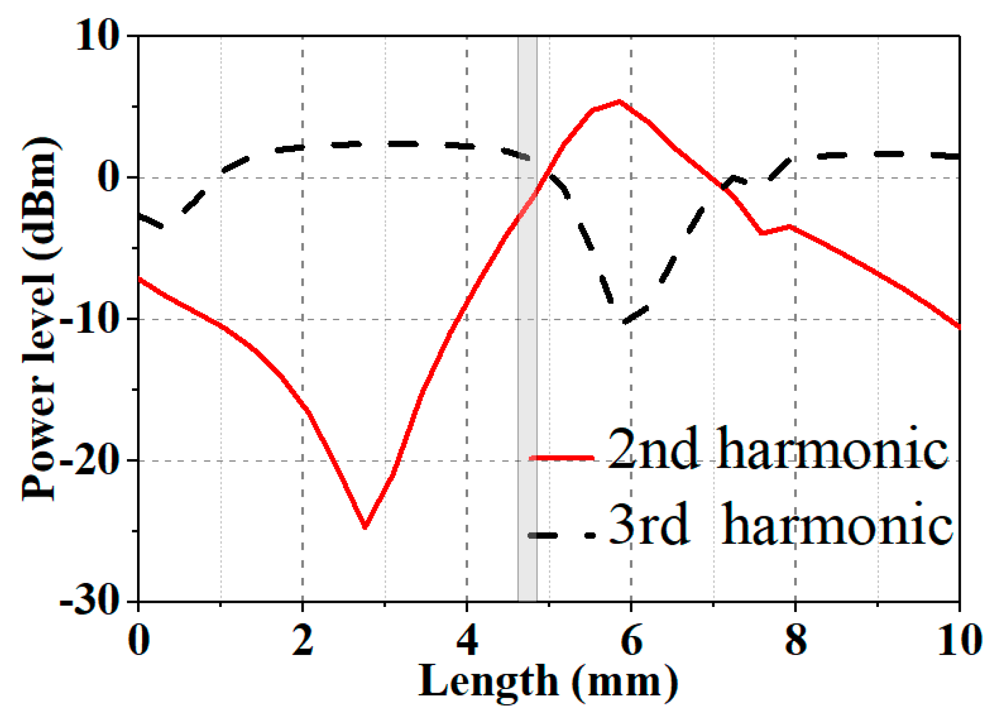
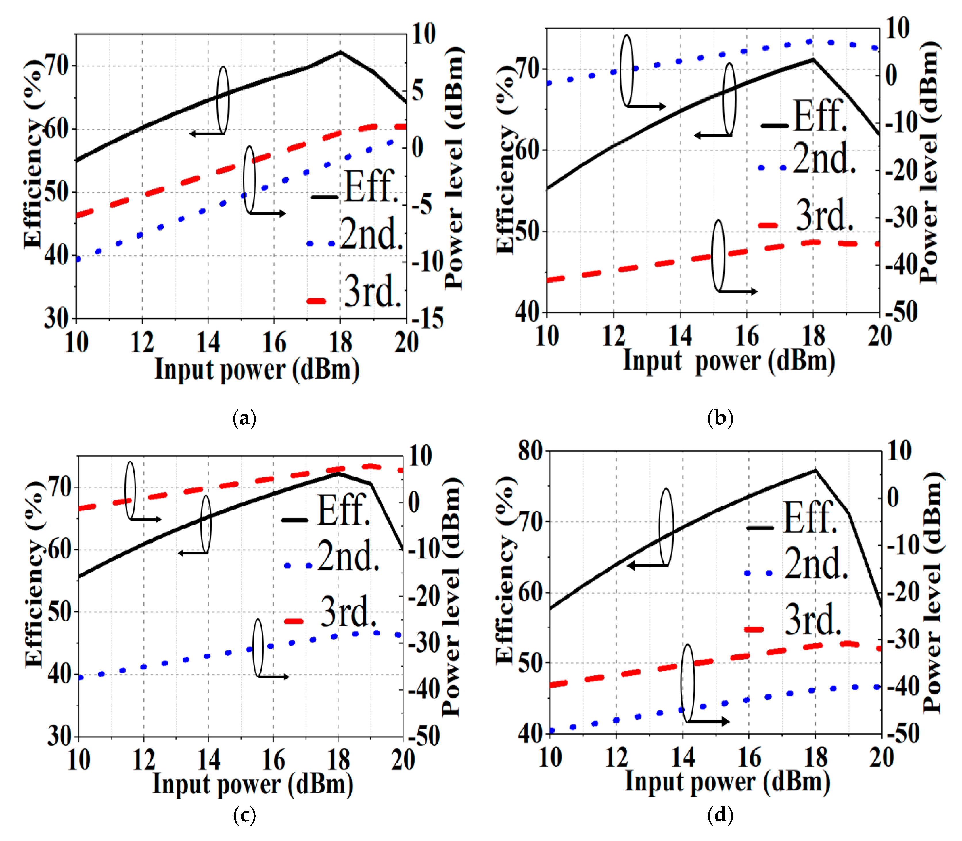
2.2. Simulation
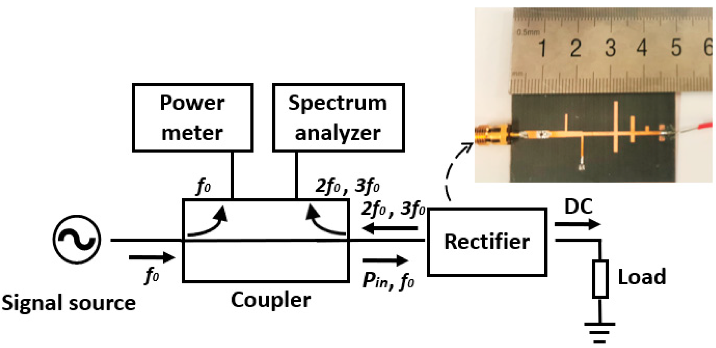
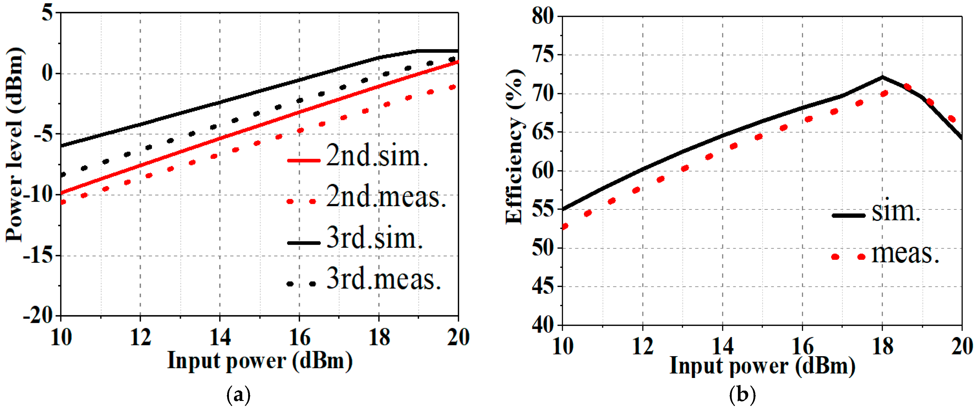
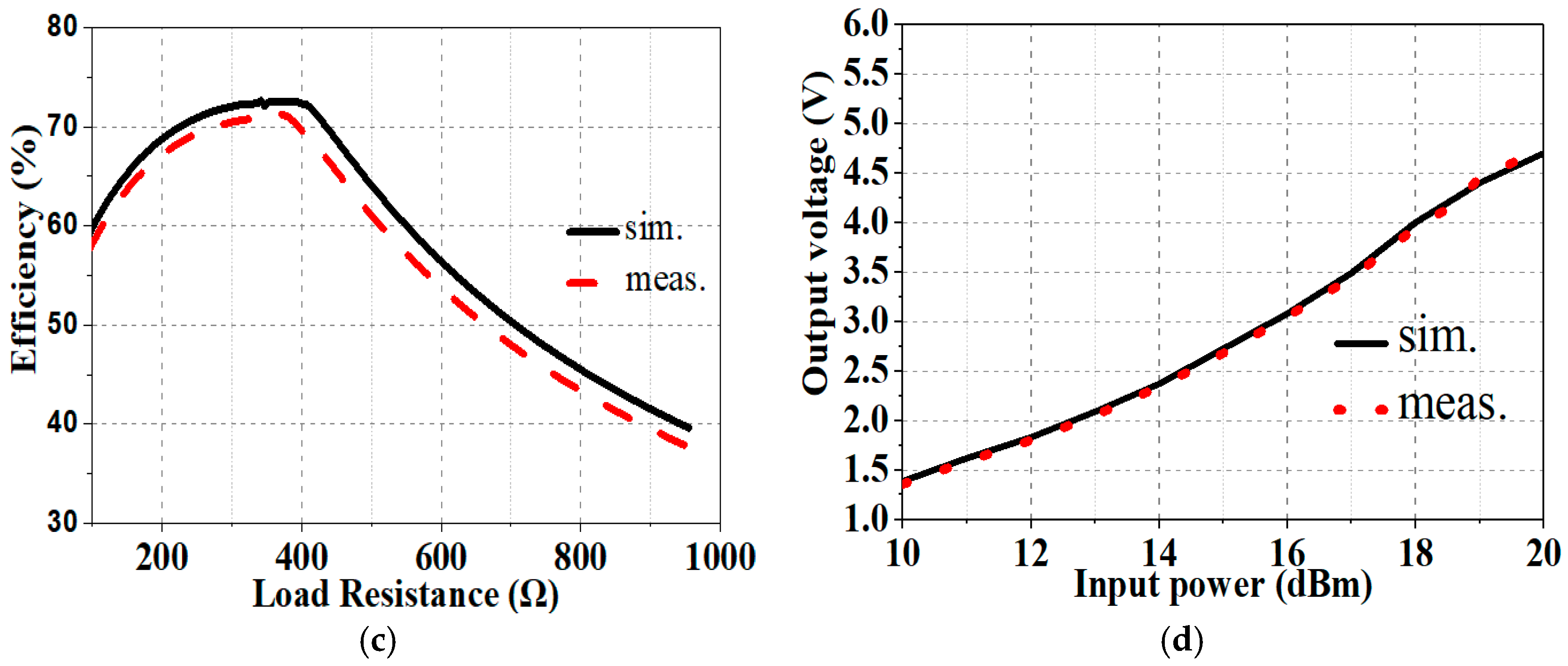
3. Experimental Validation
4. Conclusions
Author Contributions
Funding
Institutional Review Board Statement
Informed Consent Statement
Data Availability Statement
Conflicts of Interest
References
- Brown, W.C. The History of Power Transmission by Radio Waves. IEEE Trans. Microw. Theory Tech. 1984, 32, 1230–1242. [Google Scholar] [CrossRef]
- Yang, Y.; Wang, H.; Guo, Y. A Time-Modulated Array with Digitally Preprocessed Rectangular Pulses for Wireless Power Transmission. IEEE Trans. Antennas Propag. 2020, 68, 3283–3288. [Google Scholar] [CrossRef]
- Re, P.D.H.; Podilchak, S.K.; Rotenberg, S.A.; Goussetis, G.; Lee, J. Circularly Polarized Retrodirective Antenna Array for Wireless Power Transmission. IEEE Trans. Antennas Propag. 2020, 68, 2743–2752. [Google Scholar]
- Xie, L.; Shi, Y.; Hou, Y.T.; Lou, W. Wireless power transfer and applications to sensor networks. IEEE Wirel. Commun. Mag. 2013, 20, 140–145. [Google Scholar]
- Takabayashi, N.; Shinohara, N.; Mitani, T.; Furukawa, M.; Fujiwara, T. Rectification Improvement with Flat-Topped Beams on 2.45-GHz Rectenna Arrays. IEEE Trans. Microw. Theory Tech. 2020, 68, 1151–1163. [Google Scholar] [CrossRef]
- Liu, C.; Tan, F.; Zhang, H.; He, Q. A Novel Single-Diode Microwave Rectifier with a Series Band-Stop Structure. IEEE Trans. Microw. Theory Tech. 2017, 65, 600–606. [Google Scholar] [CrossRef]
- Ladan, S.; Wu, K. Nonlinear modeling and harmonic recycling of millimeter-wave rectifier circuit. IEEE Trans. Microw. Theory Tech. 2015, 63, 937–944. [Google Scholar] [CrossRef]
- Wang, C.; Shinohara, N.; Mitani, T. Study on 5.8-GHz Single-Stage Charge Pump Rectifier for Internal Wireless System of Satellite. IEEE Trans. Microw. Theory Tech. 2017, 65, 1058–1065. [Google Scholar] [CrossRef]
- Zhao, F.; Inserra, D.; Wen, G.; Li, J.; Huang, Y. A High-Efficiency Inverse Class-F Microwave Rectifier for Wireless Power Transmission. IEEE Microw. Wirel. Compon. Lett. 2019, 29, 725–728. [Google Scholar] [CrossRef]
- Zhang, H.; Guo, Y.-X.; Gao, S.-P.; Wu, W. Wireless power transfer antenna alignment using third harmonic. IEEE Microw. Wirel. Compon. Lett. 2018, 28, 536–538. [Google Scholar] [CrossRef]
- Zhang, H.; Guo, Y.-X.; Gao, S.; Zhong, Z.; Wu, W. Exploiting Third Harmonic of Differential Charge Pump for Wireless Power Transfer Antenna Alignment. IEEE Microw. Wirel. Compon. Lett. 2019, 29, 71–73. [Google Scholar] [CrossRef]
- Joseph, S.D.; Huang, Y.; Hsu, S.S.H.; Alieldin, A.; Song, C. Second Harmonic Exploitation for High-Efficiency Wireless Power Transfer Using Duplexing Rectenna. IEEE Trans. Microw. Theory Tech. 2021, 69, 482–494. [Google Scholar] [CrossRef]
- Mitani, T.; Kawashima, S.; Shinohara, N. Experimental Study on a Retrodirective System Utilizing Harmonic Reradiation from Rectenna. IEICE Trans. Electron. 2019, 102, 666–672. [Google Scholar] [CrossRef]


| Ref | Frequency (GHz) | Input Power (dBm) | Harmonic Type | Harmonic Amplitude (dBm) | Efficiency (%) | Implementation Type | Size (λg × λg) | Method |
|---|---|---|---|---|---|---|---|---|
| [10] | 2.45 | 6 | 3rd | −22 | 76% | Microstrip and lumped component | 1.16 × 1.32 | coupler |
| [11] | 2.45 | 18 | 3rd | −17.2 | 70.6% | Microstrip and lumped component | 1.28 × 1.52 | coupler |
| [12] | 0.915 | 15 | 2nd | −2 | 71% | Lumped component | 0.07 × 0.17 | separate harmonic utilization path |
| [13] | 2.45 | 10.7 | 2nd | −4.1 | 42.5% | Microstrip | N.A. | N.A. |
| This work | 5.8 | 18.3 | 2nd and 3rd | −2.4 and 0.1 | 71.3% | Microstrip | 0.69 × 1.38 | DC-pass filter |
| The Type of Harmonic Utilization | ZF, 2f0 (Ω) | ZF, 3f0 (Ω) |
|---|---|---|
| 2nd and 3rd | jX or +∞ | jX or +∞ |
| 2nd | jX or +∞ | 0 |
| 3rd | 0 | jX or +∞ |
Publisher’s Note: MDPI stays neutral with regard to jurisdictional claims in published maps and institutional affiliations. |
© 2021 by the authors. Licensee MDPI, Basel, Switzerland. This article is an open access article distributed under the terms and conditions of the Creative Commons Attribution (CC BY) license (http://creativecommons.org/licenses/by/4.0/).
Share and Cite
Qin, X.; He, G.; Yang, X.; Gao, S. A Compact Rectifier Design Method Utilizing Harmonics. Appl. Sci. 2021, 11, 2295. https://doi.org/10.3390/app11052295
Qin X, He G, Yang X, Gao S. A Compact Rectifier Design Method Utilizing Harmonics. Applied Sciences. 2021; 11(5):2295. https://doi.org/10.3390/app11052295
Chicago/Turabian StyleQin, Xuelong, Guoqiang He, Xuexia Yang, and Steven Gao. 2021. "A Compact Rectifier Design Method Utilizing Harmonics" Applied Sciences 11, no. 5: 2295. https://doi.org/10.3390/app11052295
APA StyleQin, X., He, G., Yang, X., & Gao, S. (2021). A Compact Rectifier Design Method Utilizing Harmonics. Applied Sciences, 11(5), 2295. https://doi.org/10.3390/app11052295